


Request Quote
(Ships tomorrow)
9DB401BGLF Equivalent & Substitute Parts
Part Overview
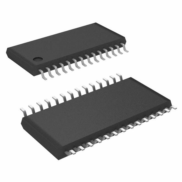
The 9DB401BGLF is a PCI Express (PCIe) Fanout Buffer IC manufactured by Renesas Electronics Corporation, designed for zero-delay distribution of clock signals in high-speed digital applications. This device features a 1:4 input-to-output ratio with differential HCSL input and HCSL/LVDS output capabilities, operating at a maximum frequency of 333.33MHz. The part is classified as obsolete, making identification of compatible substitute components essential for ongoing system support and new design implementations.
Substiute Parts
Key Parameters
| Parameter | Value |
|---|---|
| Manufacturer Part Number | 9DB401BGLF |
| Manufacturer | Renesas Electronics Corporation |
| Category | Clock/Timing |
| Description | IC BUFFER 4OUTPUT DIFF 28-TSSOP |
| Product Status | Obsolete |
| Frequency - Max | 333.33MHz |
| Input Type | HCSL |
| Output Type | HCSL, LVDS |
| Ratio - Input:Output | 1:4 |
| Differential - Input:Output | Yes/Yes |
| Voltage - Supply | 3.135V ~ 3.465V |
| Operating Temperature | 0°C ~ 70°C |
| Package / Case | 28-TSSOP (0.173", 4.40mm Width) |
| Mounting Type | Surface Mount |
| Moisture Sensitivity Level (MSL) | 1 (Unlimited) |
Substitute Part Grouping Explanation
The 9DB403DGLF qualifies as a direct substitute for the 9DB401BGLF based on the following critical parameters:
- Package Compatibility: Both devices use 28-TSSOP surface mount packaging with identical physical dimensions (0.173", 4.40mm Width)
- Signal Interface: Both feature differential HCSL input and HCSL/LVDS output configuration
- Circuit Architecture: Both implement 1:4 input-to-output ratio with single circuit configuration
- Electrical Specifications: Both operate within the same supply voltage range (3.135V ~ 3.465V) and temperature range (0°C ~ 70°C)
- Differential Signaling: Both support differential input and output signaling
- PLL Integration: Both include integrated PLL functionality
The 9DB403DGLF provides enhanced frequency capability (400MHz maximum versus 333.33MHz), representing a performance upgrade while maintaining full backward compatibility with the 9DB401BGLF pinout and electrical interface.
Parameter Comparison
| Parameter | 9DB401BGLF | 9DB403DGLF |
|---|---|---|
| Manufacturer Part Number | 9DB401BGLF | 9DB403DGLF |
| Manufacturer | Renesas Electronics Corporation | Renesas Electronics Corporation |
| Category | Clock/Timing | Clock/Timing |
| Product Status | Obsolete | Active |
| Frequency - Max | 333.33MHz | 400MHz |
| Input Type | HCSL | HCSL |
| Output Type | HCSL, LVDS | HCSL, LVDS |
| Ratio - Input:Output | 1:4 | 1:4 |
| Differential - Input:Output | Yes/Yes | Yes/Yes |
| Voltage - Supply | 3.135V ~ 3.465V | 3.135V ~ 3.465V |
| Operating Temperature | 0°C ~ 70°C | 0°C ~ 70°C |
| Package / Case | 28-TSSOP (0.173", 4.40mm Width) | 28-TSSOP (0.173", 4.40mm Width) |
| Mounting Type | Surface Mount | Surface Mount |
| Moisture Sensitivity Level (MSL) | 1 (Unlimited) | 1 (Unlimited) |
| PLL | Yes | Yes |
Engineering Selection Recommendations
The 9DB403DGLF is the appropriate substitute for the obsolete 9DB401BGLF. The 9DB403DGLF maintains active product status with Renesas Electronics Corporation, ensuring ongoing availability and manufacturing support. Both devices share identical pinout, package dimensions, and electrical interface specifications, enabling direct replacement without PCB redesign.
The 9DB403DGLF provides increased maximum frequency specification (400MHz versus 333.33MHz), which represents a performance enhancement for applications operating at or below the original 333.33MHz specification. The device maintains compliance with REACH regulations and EAR99 export classification consistent with the original part.
Frequently Asked Questions (FAQ)
Q: Can the 9DB403DGLF directly replace the 9DB401BGLF on existing PCBs?
A: Yes. Both devices use identical 28-TSSOP packaging with matching pinout, supply voltage range (3.135V ~ 3.465V), and operating temperature range (0°C ~ 70°C). No PCB modifications are required.
Q: What is the primary difference between these two parts?
A: The 9DB403DGLF supports a maximum frequency of 400MHz compared to the 9DB401BGLF's 333.33MHz specification. The 9DB403DGLF is also in active production status, whereas the 9DB401BGLF is obsolete.
Q: Are the input and output signal types identical?
A: Yes. Both devices feature differential HCSL input and HCSL/LVDS output configuration with a 1:4 input-to-output ratio.
Q: Does the 9DB403DGLF require different supply voltage?
A: No. Both parts operate within the same supply voltage range of 3.135V ~ 3.465V.
Q: What is the moisture sensitivity level for both parts?
A: Both the 9DB401BGLF and 9DB403DGLF have MSL 1 (Unlimited), indicating no moisture sensitivity restrictions.
Alternative Parts

SJ6012L2TP
Littelfuse Inc.
6 Alternative Parts

JMK107BBJ476MA-RE
Taiyo Yuden
10 Alternative Parts

GMK107BBJ475MA-T
Taiyo Yuden
5 Alternative Parts
SJ6020N2ARP
Littelfuse Inc.
3 Alternative Parts
SJ6025R2ATP
Littelfuse Inc.
4 Alternative Parts

2474-05L
API Delevan Inc.
1 Alternative Parts

4590R-684K
API Delevan Inc.
1 Alternative Parts

CM6560R-334
API Delevan Inc.
1 Alternative Parts

CM6460-104
API Delevan Inc.
1 Alternative Parts

5526-12
API Delevan Inc.
1 Alternative Parts