


Request Quote
(Ships tomorrow)
9DB108BGLF Equivalent & Substitute Parts
Part Overview
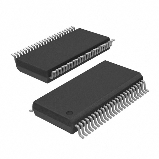
The 9DB108BGLF is a PCI Express (PCIe) Clock Buffer/Driver IC manufactured by Renesas Electronics Corporation, designed to distribute clock signals across PCIe applications. This 48-TSSOP surface mount device operates at a maximum frequency of 220MHz with a 1:8 input-to-output ratio and differential signaling on both input and output. The device is classified as obsolete, making identification of compatible substitute parts essential for ongoing system support and new design implementations where legacy component replacement is required.
Substiute Parts
Key Parameters
| Parameter | Value |
|---|---|
| Manufacturer Part Number | 9DB108BGLF |
| Manufacturer | Renesas Electronics Corporation |
| Category | Clock/Timing |
| Product Status | Obsolete |
| Main Purpose | PCI Express (PCIe) |
| Frequency - Max | 220MHz |
| Ratio - Input:Output | 1:8 |
| Differential - Input:Output | Yes/Yes |
| Voltage - Supply | 3.135V ~ 3.465V |
| Operating Temperature | 0°C ~ 70°C |
| Package / Case | 48-TFSOP (0.240", 6.10mm Width) |
| Mounting Type | Surface Mount |
| RoHS Status | ROHS3 Compliant |
| Moisture Sensitivity Level (MSL) | 1 (Unlimited) |
Substitute Part Grouping Explanation
Substitution of the 9DB108BGLF is determined by the following critical parameters:
- Functional Category: PCI Express (PCIe) clock distribution
- Input/Output Ratio: 1:8 fanout capability
- Differential Signaling: Both input and output must support differential signal transmission
- Frequency Range: Maximum operating frequency must meet or exceed 220MHz
- Supply Voltage Compatibility: Operating voltage range must overlap with or encompass the original specification (3.135V ~ 3.465V)
- Surface Mount Packaging: Substitute must be surface mount compatible
- Compliance Standards: RoHS3 compliance required for modern manufacturing environments
The RC19008A100GND#BB0 qualifies as a substitute based on these parameters, despite differences in package form factor and extended operating temperature range.
Parameter Comparison
| Parameter | 9DB108BGLF (Main Part) | RC19008A100GND#BB0 (Substitute) |
|---|---|---|
| Manufacturer | Renesas Electronics Corporation | Renesas Electronics Corporation |
| Category | Clock/Timing | Clock/Timing |
| Main Purpose | PCI Express (PCIe) | PCI Express (PCIe) |
| Ratio - Input:Output | 1:8 | 1:8 |
| Differential - Input:Output | Yes/Yes | Yes/Yes |
| Frequency - Max | 220MHz | 400MHz |
| Voltage - Supply | 3.135V ~ 3.465V | 2.97V ~ 3.63V |
| Operating Temperature | 0°C ~ 70°C | -40°C ~ 105°C (TA) |
| Mounting Type | Surface Mount | Surface Mount |
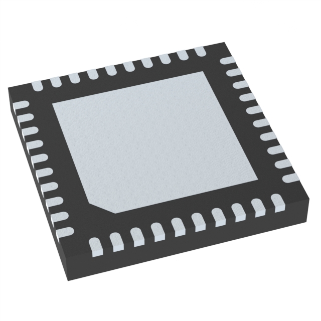
| Package / Case | 48-TFSOP (0.240", 6.10mm Width) | 40-VFQFN Exposed Pad (5x5) |
| RoHS Status | ROHS3 Compliant | ROHS3 Compliant |
| Product Status | Obsolete | Active |
Engineering Selection Recommendations
The RC19008A100GND#BB0 serves as a functional substitute for the obsolete 9DB108BGLF in PCIe clock distribution applications. Both devices are manufactured by Renesas Electronics Corporation and maintain ROHS3 compliance, ensuring regulatory alignment for current manufacturing standards.
The substitute part exceeds the original specification in maximum frequency (400MHz versus 220MHz) and extends the operating temperature range (-40°C to 105°C versus 0°C to 70°C), providing enhanced performance margins for demanding applications. The supply voltage range of the substitute (2.97V ~ 3.63V) encompasses the original specification range (3.135V ~ 3.465V), ensuring compatibility with existing power delivery systems.
The primary design consideration is the package transition from 48-TFSOP to 40-VFQFN. This change requires PCB layout modification and component footprint redesign. The reduced pin count (40 versus 48) and different physical dimensions necessitate electrical schematic review to confirm signal routing compatibility.
Both parts maintain the critical 1:8 input-to-output ratio and differential signaling architecture required for PCIe applications, establishing functional equivalence at the system level.
Frequently Asked Questions (FAQ)
Q: Can the RC19008A100GND#BB0 directly replace the 9DB108BGLF without PCB modification?
A: No. The package change from 48-TFSOP to 40-VFQFN requires PCB footprint redesign. Pin assignments must be verified against both datasheets to ensure correct signal routing.
Q: What is the significance of the frequency difference (220MHz versus 400MHz)?
A: The substitute operates at twice the maximum frequency of the original part. This provides performance headroom but does not create incompatibility. The substitute will function correctly in applications designed for 220MHz operation.
Q: Are the supply voltage ranges compatible?
A: Yes. The substitute voltage range (2.97V ~ 3.63V) overlaps with and extends beyond the original range (3.135V ~ 3.465V). Existing power supply designs will operate within the substitute's specifications.
Q: Why does the substitute have a wider operating temperature range?
A: The RC19008A100GND#BB0 is an active product with extended specifications for broader application support. The original 9DB108BGLF, being obsolete, had more limited environmental ratings. The extended range of the substitute provides additional design flexibility.
Q: What does the package designation "40-VFQFN Exposed Pad" mean?
A: VFQFN indicates a Very Fine Pitch Quad Flat No-Lead package. The exposed pad provides thermal management and ground connection. This differs from the TFSOP package, which uses traditional lead-based termination.
Q: Is the 1:8 ratio maintained in the substitute?
A: Yes. Both the 9DB108BGLF and RC19008A100GND#BB0 maintain a 1:8 input-to-output ratio, preserving the fanout capability required for PCIe clock distribution.
Q: Are both parts RoHS compliant?
A: Yes. Both devices are ROHS3 compliant, meeting current environmental and regulatory requirements for electronic component manufacturing and assembly.
Alternative Parts

SJ6012L2TP
Littelfuse Inc.
6 Alternative Parts

JMK107BBJ476MA-RE
Taiyo Yuden
10 Alternative Parts

GMK107BBJ475MA-T
Taiyo Yuden
5 Alternative Parts
SJ6020N2ARP
Littelfuse Inc.
3 Alternative Parts
SJ6025R2ATP
Littelfuse Inc.
4 Alternative Parts

2474-05L
API Delevan Inc.
1 Alternative Parts

4590R-684K
API Delevan Inc.
1 Alternative Parts

CM6560R-334
API Delevan Inc.
1 Alternative Parts

CM6460-104
API Delevan Inc.
1 Alternative Parts

5526-12
API Delevan Inc.
1 Alternative Parts