


Request Quote
(Ships tomorrow)
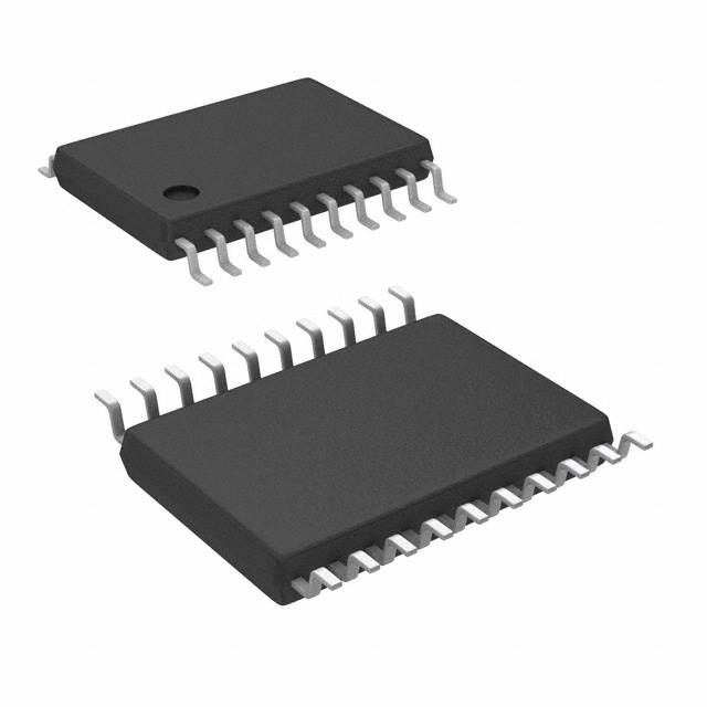
8536CGI-33LF Clock Fanout Buffer Equivalent & Substitute Parts
Part Overview
The 8536CGI-33LF is a Clock Fanout Buffer (Distribution), Multiplexer IC manufactured by Renesas Electronics Corporation. This device functions as a 2:6 clock distribution buffer with a maximum frequency of 266 MHz, designed for surface mount applications in 20-TSSOP packaging. The part is classified as Obsolete, making identification of suitable substitute components necessary for ongoing system support and new design implementations where this device is specified.
Substiute Parts
Key Parameters
| Parameter | Value |
|---|---|
| Manufacturer Part Number | 8536CGI-33LF |
| Manufacturer | Renesas Electronics Corporation |
| Category | Clock/Timing |
| Type | Fanout Buffer (Distribution), Multiplexer |
| Ratio - Input:Output | 2:6 |
| Frequency - Max | 266 MHz |
| Voltage - Supply | 2.375V ~ 3.465V |
| Operating Temperature | -40°C ~ 85°C |
| Package / Case | 20-TSSOP (0.173", 4.40mm Width) |
| Mounting Type | Surface Mount |
| Product Status | Obsolete |
| RoHS Status | ROHS3 Compliant |
| Moisture Sensitivity Level (MSL) | 1 (Unlimited) |
Substitute Part Grouping Explanation
Substitution of the 8536CGI-33LF is determined by the following critical parameters:
- Input/Output Ratio: The 2:6 configuration (2 inputs, 6 outputs) defines the distribution capability
- Maximum Frequency: 266 MHz operational ceiling for clock distribution
- Supply Voltage Range: 2.375V ~ 3.465V compatibility window
- Input/Output Signal Types: LVCMOS, LVTTL, Crystal inputs with LVCMOS, LVPECL outputs
- Package Type: 20-TSSOP surface mount form factor
- Operating Temperature Range: -40°C ~ 85°C specification
The identified substitute part, 5P83905PGGK, differs in input/output ratio (1:6 vs. 2:6), maximum frequency (200 MHz vs. 266 MHz), package size (16-TSSOP vs. 20-TSSOP), and signal type support. These differences require engineering evaluation for specific application requirements.
Parameter Comparison
| Parameter | 8536CGI-33LF (Main Part) | 5P83905PGGK (Substitute) |
|---|---|---|
| Manufacturer | Renesas Electronics Corporation | Renesas Electronics Corporation |
| Category | Clock/Timing | Clock/Timing |
| Type | Fanout Buffer (Distribution), Multiplexer | Fanout Buffer (Distribution) |
| Ratio - Input:Output | 2:6 | 1:6 |
| Frequency - Max | 266 MHz | 200 MHz |
| Voltage - Supply | 2.375V ~ 3.465V | 1.71V ~ 3.465V |
| Operating Temperature | -40°C ~ 85°C | -40°C ~ 105°C |
| Input Signal Type | LVCMOS, LVTTL, Crystal | Crystal |
| Output Signal Type | LVCMOS, LVPECL | LVCMOS |
| Package / Case | 20-TSSOP (0.173", 4.40mm Width) | 16-TSSOP (0.173", 4.40mm Width) |
| Mounting Type | Surface Mount | Surface Mount |
| Product Status | Obsolete | Active |
| RoHS Status | ROHS3 Compliant | ROHS3 Compliant |
| Moisture Sensitivity Level (MSL) | 1 (Unlimited) | 1 (Unlimited) |
Engineering Selection Recommendations
The 5P83905PGGK is an Active product from Renesas Electronics Corporation, providing ongoing manufacturing support and availability compared to the Obsolete 8536CGI-33LF. Both components maintain ROHS3 compliance and MSL Level 1 ratings, ensuring equivalent environmental and regulatory standing.
Selection of the 5P83905PGGK requires verification that the application can accommodate the following parameter differences: reduced input/output ratio (1:6 vs. 2:6), lower maximum frequency (200 MHz vs. 266 MHz), restricted input signal type support (Crystal only vs. LVCMOS, LVTTL, Crystal), and reduced output signal type support (LVCMOS only vs. LVCMOS, LVPECL). The substitute part offers extended operating temperature range (-40°C ~ 105°C vs. -40°C ~ 85°C) and lower minimum supply voltage (1.71V vs. 2.375V).
Frequently Asked Questions (FAQ)
Q: Can the 5P83905PGGK directly replace the 8536CGI-33LF in existing designs?
A: Direct replacement requires application-level compatibility verification. The substitute part has a different input/output ratio (1:6 vs. 2:6), lower maximum frequency (200 MHz vs. 266 MHz), and different signal type support. PCB layout modifications may be necessary due to package size difference (16-TSSOP vs. 20-TSSOP).
Q: What are the key differences in signal compatibility?
A: The 8536CGI-33LF accepts LVCMOS, LVTTL, and Crystal inputs with LVCMOS and LVPECL outputs. The 5P83905PGGK accepts Crystal inputs only with LVCMOS outputs. Applications requiring LVTTL or LVPECL signal support cannot use the substitute without additional signal conditioning circuitry.
Q: Does the package size difference affect PCB compatibility?
A: Yes. The 8536CGI-33LF uses 20-TSSOP packaging while the 5P83905PGGK uses 16-TSSOP packaging. Both maintain the same 0.173" width, but pin count and footprint differ. PCB redesign is required for substitution.
Q: Are both parts compliant with current environmental standards?
A: Both the 8536CGI-33LF and 5P83905PGGK are ROHS3 compliant with MSL Level 1 ratings, meeting current environmental and moisture sensitivity requirements.
Q: What is the frequency limitation impact of using the 5P83905PGGK?
A: The substitute part operates at a maximum frequency of 200 MHz compared to the main part's 266 MHz. Applications requiring clock distribution above 200 MHz cannot use this substitute.
Alternative Parts

SJ6012L2TP
Littelfuse Inc.
6 Alternative Parts

JMK107BBJ476MA-RE
Taiyo Yuden
10 Alternative Parts

GMK107BBJ475MA-T
Taiyo Yuden
5 Alternative Parts
SJ6020N2ARP
Littelfuse Inc.
3 Alternative Parts
SJ6025R2ATP
Littelfuse Inc.
4 Alternative Parts

2474-05L
API Delevan Inc.
1 Alternative Parts

4590R-684K
API Delevan Inc.
1 Alternative Parts

CM6560R-334
API Delevan Inc.
1 Alternative Parts

CM6460-104
API Delevan Inc.
1 Alternative Parts

5526-12
API Delevan Inc.
1 Alternative Parts