


Request Quote
(Ships tomorrow)
Equivalent & Substitute Parts for 8516FYILF
Part Overview
The 8516FYILF is a Clock Fanout Buffer (Distribution) IC manufactured by Renesas Electronics Corporation, designed for 1:16 clock distribution at frequencies up to 700 MHz. This device features differential input and output capabilities with support for multiple input standards including HCSL, LVDS, LVHSTL, LVPECL, and SSTL, outputting LVDS signals. The part is classified as obsolete, making identification of suitable substitute components essential for ongoing system design and maintenance.
Substiute Parts
Key Parameters
| Parameter | Value |
|---|---|
| Manufacturer Part Number | 8516FYILF |
| Manufacturer | Renesas Electronics Corporation |
| Category | Clock/Timing |
| Type | Fanout Buffer (Distribution) |
| Number of Circuits | 1 |
| Ratio - Input:Output | 1:16 |
| Differential - Input:Output | Yes/Yes |
| Input Standards | HCSL, LVDS, LVHSTL, LVPECL, SSTL |
| Output Standard | LVDS |
| Frequency - Max | 700 MHz |
| Voltage - Supply | 3.135V ~ 3.465V |
| Operating Temperature | -40°C ~ 85°C |
| Mounting Type | Surface Mount |
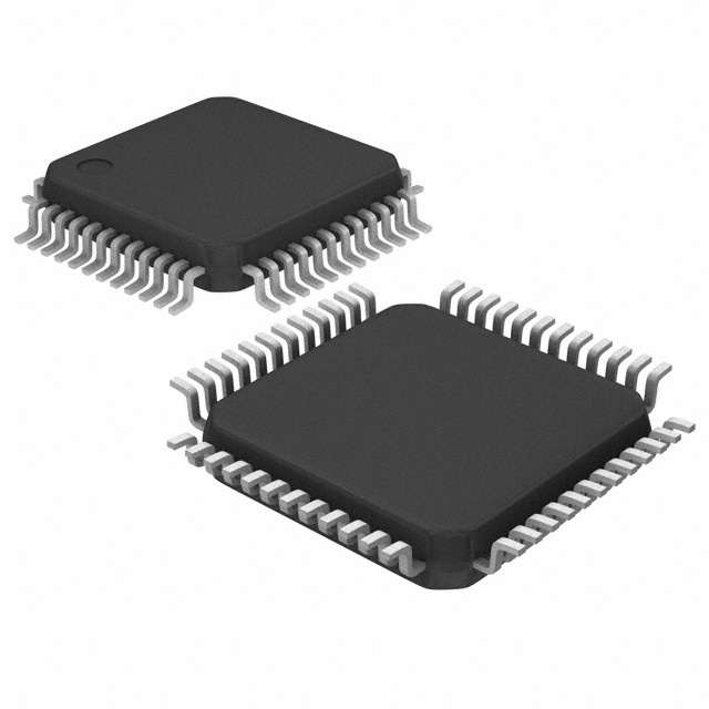
| Package / Case | 48-LQFP |
| Product Status | Obsolete |
| RoHS Status | ROHS3 Compliant |
| MSL Rating | 3 (168 Hours) |
Substitute Part Grouping Explanation
Substitution of the 8516FYILF requires evaluation based on the following critical parameters:
Functional Compatibility Criteria:
- Type: Fanout Buffer (Distribution) IC
- Differential Input/Output capability: Yes/Yes
- Output Standard: LVDS
- Operating Temperature Range: -40°C ~ 85°C
- Surface Mount packaging capability
Performance Considerations:
- Maximum frequency capability must meet or exceed application requirements
- Supply voltage range must be compatible with system design
- Input standard compatibility with existing signal sources
Compliance & Certification:
- RoHS3 compliance status
- MSL rating for manufacturing processes
- REACH compliance status
The 8P34S2108NLGI qualifies as a substitute based on shared functional architecture, differential I/O capability, LVDS output standard, matching operating temperature range, and equivalent compliance certifications. However, key differences exist in circuit count, input/output ratio, frequency capability, and supply voltage specifications that must be evaluated against specific application requirements.
Parameter Comparison
| Parameter | 8516FYILF (Main Part) | 8P34S2108NLGI (Substitute) |
|---|---|---|
| Manufacturer | Renesas Electronics Corporation | Renesas Electronics Corporation |
| Type | Fanout Buffer (Distribution) | Fanout Buffer (Distribution) |
| Number of Circuits | 1 | 2 |
| Ratio - Input:Output | 1:16 | 2:16 |
| Differential - Input:Output | Yes/Yes | Yes/Yes |
| Output Standard | LVDS | LVDS |
| Frequency - Max | 700 MHz | 2 GHz |
| Voltage - Supply | 3.135V ~ 3.465V | 1.71V ~ 1.89V |
| Operating Temperature | -40°C ~ 85°C | -40°C ~ 85°C |
| Mounting Type | Surface Mount | Surface Mount |
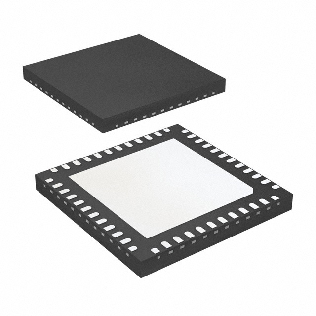
| Package / Case | 48-LQFP | 48-VFQFN Exposed Pad |
| Product Status | Obsolete | Active |
| RoHS Status | ROHS3 Compliant | ROHS3 Compliant |
| MSL Rating | 3 (168 Hours) | 3 (168 Hours) |
Engineering Selection Recommendations
Product Status Consideration: The 8516FYILF is classified as obsolete, necessitating transition to active production parts. The 8P34S2108NLGI maintains active product status with Renesas Electronics Corporation, ensuring continued availability and manufacturing support.
Compliance & Certification Alignment: Both parts maintain ROHS3 compliance and equivalent MSL ratings, satisfying regulatory and manufacturing process requirements. REACH compliance status is unaffected for both components.
Functional Architecture: Both devices are Fanout Buffer (Distribution) ICs with differential input and output capability and LVDS output standard. The 8P34S2108NLGI provides enhanced frequency capability (2 GHz versus 700 MHz) and dual-circuit architecture (2:16 ratio versus 1:16 ratio), offering greater flexibility for multi-channel clock distribution applications.
Supply Voltage Compatibility: The 8P34S2108NLGI operates at 1.71V ~ 1.89V supply voltage, differing from the 8516FYILF specification of 3.135V ~ 3.465V. System power supply architecture must accommodate this voltage requirement.
Package Transition: The 8P34S2108NLGI uses 48-VFQFN Exposed Pad packaging compared to the 8516FYILF 48-LQFP package. Both are 48-pin surface mount packages with 7x7mm footprints, though PCB layout modifications may be required due to package geometry differences.
Frequently Asked Questions (FAQ)
Q: Can the 8P34S2108NLGI directly replace the 8516FYILF without circuit modifications?
A: Direct replacement requires evaluation of three critical factors: (1) Supply voltage compatibility—the substitute operates at 1.71V ~ 1.89V versus the original 3.135V ~ 3.465V, necessitating power supply redesign; (2) Package geometry—48-VFQFN Exposed Pad differs from 48-LQFP, requiring PCB layout changes; (3) Dual-circuit architecture—the substitute provides 2:16 distribution versus 1:16, offering additional functionality but requiring signal routing assessment.
Q: What input standards does the 8P34S2108NLGI support?
A: The 8P34S2108NLGI supports LVCMOS, LVDS, and LVPECL input standards. The original 8516FYILF supports HCSL, LVDS, LVHSTL, LVPECL, and SSTL. Input standard compatibility must be confirmed with existing signal sources in the application.
Q: Are both parts suitable for the same frequency range?
A: No. The 8516FYILF operates to 700 MHz maximum, while the 8P34S2108NLGI operates to 2 GHz maximum. The substitute provides higher frequency capability, suitable for applications requiring frequencies up to 2 GHz. For applications limited to 700 MHz or below, the substitute's enhanced frequency capability does not impose constraints.
Q: What are the compliance differences between these parts?
A: Both parts maintain ROHS3 compliance, equivalent MSL ratings (3, 168 Hours), and REACH unaffected status. Compliance certifications are equivalent for regulatory and manufacturing process requirements.
Q: How does the dual-circuit architecture of the 8P34S2108NLGI affect system design?
A: The 8P34S2108NLGI provides two independent 2:16 distribution circuits versus the single 1:16 circuit of the 8516FYILF. This enables multi-channel clock distribution from a single device, reducing component count. System design must account for the additional output channels and associated signal routing.
Q: What packaging considerations apply to this substitution?
A: The 8P34S2108NLGI uses 48-VFQFN Exposed Pad packaging with an exposed thermal pad, compared to the 8516FYILF 48-LQFP package. Both are 7x7mm footprints, but pin layout and thermal management characteristics differ. PCB layout redesign is required, including thermal pad connection strategy for the substitute part.
Alternative Parts

SJ6012L2TP
Littelfuse Inc.
6 Alternative Parts

JMK107BBJ476MA-RE
Taiyo Yuden
10 Alternative Parts

GMK107BBJ475MA-T
Taiyo Yuden
5 Alternative Parts
SJ6020N2ARP
Littelfuse Inc.
3 Alternative Parts
SJ6025R2ATP
Littelfuse Inc.
4 Alternative Parts

2474-05L
API Delevan Inc.
1 Alternative Parts

4590R-684K
API Delevan Inc.
1 Alternative Parts

CM6560R-334
API Delevan Inc.
1 Alternative Parts

CM6460-104
API Delevan Inc.
1 Alternative Parts

5526-12
API Delevan Inc.
1 Alternative Parts