


Request Quote
(Ships tomorrow)
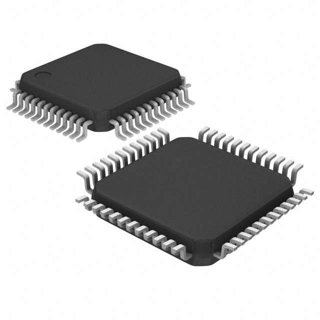
849S625BYILF Clock Synthesizer IC Equivalent & Substitute Parts
Part Overview
The 849S625BYILF is a Clock Synthesizer IC manufactured by Renesas Electronics Corporation, designed for high-frequency timing applications requiring up to 625MHz output. This device features integrated Phase-Locked Loop (PLL) with bypass capability, supporting multiple input standards (LVCMOS, LVTTL, Crystal) and differential LVDS/LVPECL outputs. The part is classified as Obsolete, necessitating identification of functionally equivalent alternatives for new designs and production continuity.
Substiute Parts
Key Parameters
| Parameter | 849S625BYILF |
|---|---|
| Manufacturer | Renesas Electronics Corporation |
| Category | Clock/Timing |
| Type | Clock Synthesizer |
| Frequency - Max | 625MHz |
| PLL | Yes with Bypass |
| Input Standards | LVCMOS, LVTTL, Crystal |
| Output Standards | LVDS, LVPECL |
| Number of Circuits | 1 |
| Ratio - Input:Output | 2:10 |
| Differential Output | Yes |
| Voltage - Supply | 3.135V ~ 3.465V |
| Operating Temperature | -40°C ~ 85°C |
| Package / Case | 48-LQFP |
| Mounting Type | Surface Mount |
| Product Status | Obsolete |
| RoHS Status | ROHS3 Compliant |
| MSL Rating | 3 (168 Hours) |
Substitute Part Grouping Explanation
Substitution of the 849S625BYILF is determined by the following critical parameters:
Functional Requirements:
- Clock synthesis capability with integrated PLL and bypass mode
- Maximum frequency support of 625MHz or higher
- Single circuit configuration
- Differential output capability (LVDS/LVPECL compatible)
Electrical Compatibility:
- Supply voltage range overlap or compatibility with 3.135V ~ 3.465V
- Operating temperature range of -40°C ~ 85°C minimum
- Input standard support for LVCMOS, LVTTL, or Crystal sources
- Output standard support for LVDS or LVPECL
Physical & Compliance Requirements:
- Surface mount packaging
- ROHS3 compliance
- MSL rating of 3 or better
- Similar or smaller package footprint (48-LQFP baseline)
The RC21008A000GND#BB0 qualifies as a substitute based on these criteria: it maintains clock synthesis functionality with PLL, supports higher maximum frequency (650MHz), provides compatible supply voltage options including the 3.135V ~ 3.465V range, maintains the -40°C ~ 85°C operating temperature range, and meets all compliance requirements.
Parameter Comparison
| Parameter | 849S625BYILF | RC21008A000GND#BB0 | Compatibility Notes |
|---|---|---|---|
| Manufacturer | Renesas Electronics Corporation | Renesas Electronics Corporation | Same manufacturer |
| Category | Clock/Timing | Clock/Timing | Equivalent category |
| Type | Clock Synthesizer | Clock Generator | Both provide clock synthesis with PLL |
| Frequency - Max | 625MHz | 650MHz | Substitute supports higher frequency |
| PLL | Yes with Bypass | Yes | Both include PLL functionality |
| Input Standards | LVCMOS, LVTTL, Crystal | CML, HCSL, LVCMOS, LVDS, LVPECL, Crystal | Substitute supports broader input options |
| Output Standards | LVDS, LVPECL | LP-HCSL, LVCMOS, LVDS | Substitute supports LVDS; verify LVPECL requirement |
| Number of Circuits | 1 | 1 | Equivalent |
| Differential Output | Yes | Yes | Both support differential outputs |
| Voltage - Supply | 3.135V ~ 3.465V | 1.71V ~ 1.89V, 2.375V ~ 2.625V, 3.135V ~ 3.465V | Substitute includes compatible 3.3V range |
| Operating Temperature | -40°C ~ 85°C | -40°C ~ 85°C | Equivalent |
| Package / Case | 48-LQFP | 40-VFQFN Exposed Pad | Different package; PCB layout redesign required |
| Mounting Type | Surface Mount | Surface Mount | Equivalent |
| Product Status | Obsolete | Active | Substitute is in active production |
| RoHS Status | ROHS3 Compliant | ROHS3 Compliant | Equivalent compliance |
| MSL Rating | 3 (168 Hours) | 3 (168 Hours) | Equivalent moisture sensitivity |
Engineering Selection Recommendations
The RC21008A000GND#BB0 is suitable as a substitute for the obsolete 849S625BYILF based on the following engineering criteria:
Product Status & Availability: The 849S625BYILF is classified as Obsolete, making long-term supply and support unavailable. The RC21008A000GND#BB0 maintains Active product status with current manufacturing support from Renesas Electronics Corporation.
Compliance & Certifications: Both parts maintain ROHS3 compliance and equivalent MSL ratings (3, 168 Hours), ensuring compatibility with modern manufacturing and environmental standards. Both carry EAR99 ECCN classification and REACH Unaffected status.
Functional Equivalence: The substitute provides clock synthesis with integrated PLL, matching the core functionality of the original part. The higher maximum frequency (650MHz vs. 625MHz) provides additional performance headroom for timing-critical applications.
Supply Voltage Compatibility: The RC21008A000GND#BB0 includes the 3.135V ~ 3.465V supply range required by the original design, along with additional voltage options for flexible system integration.
Package Consideration: The substitute uses a 40-VFQFN package versus the original 48-LQFP. This represents a smaller footprint but requires PCB layout redesign and verification of signal integrity for the new pinout configuration.
Frequently Asked Questions (FAQ)
Q: Can the RC21008A000GND#BB0 directly replace the 849S625BYILF without PCB modifications?
A: No. The substitute uses a different package (40-VFQFN vs. 48-LQFP) with a different pinout. PCB layout redesign is required, including trace routing, via placement, and decoupling capacitor repositioning. Schematic review is necessary to verify signal assignments.
Q: What is the key difference between Clock Synthesizer and Clock Generator classifications?
A: Both device types incorporate PLL-based frequency synthesis. The functional distinction in this context is minimal; both parts generate output clocks from input references through multiplication/division ratios. The RC21008A000GND#BB0 provides equivalent synthesis capability.
Q: Does the RC21008A000GND#BB0 support LVPECL output like the original part?
A: The RC21008A000GND#BB0 specifies LP-HCSL, LVCMOS, and LVDS output standards. LVPECL output is not listed in the provided specifications. If LVPECL output is a critical requirement, output signal compatibility must be verified through detailed datasheet review and application circuit analysis.
Q: Are the input/output ratio specifications compatible?
A: The original part specifies a 2:10 input:output ratio. The substitute specifies a 3:8 ratio. These ratios represent different frequency multiplication/division configurations. Application-specific frequency requirements must be verified against the substitute's programmable ratio capabilities.
Q: What is the significance of the Exposed Pad in the 40-VFQFN package?
A: The exposed pad provides thermal and electrical grounding. This design feature improves heat dissipation compared to non-exposed pad packages. PCB layout must include proper thermal via placement and copper area connection to the exposed pad for optimal thermal performance.
Q: Are both parts suitable for the same operating temperature range?
A: Yes. Both parts specify -40°C ~ 85°C operating temperature range, ensuring equivalent thermal performance across industrial and commercial temperature specifications.
Q: What inventory status should be considered for production planning?
A: The original 849S625BYILF shows 2100 pieces in stock but is Obsolete. The RC21008A000GND#BB0 shows 750 pieces in stock with Active product status, indicating ongoing availability and manufacturing support for future production runs.
Alternative Parts

SJ6012L2TP
Littelfuse Inc.
6 Alternative Parts

JMK107BBJ476MA-RE
Taiyo Yuden
10 Alternative Parts

GMK107BBJ475MA-T
Taiyo Yuden
5 Alternative Parts
SJ6020N2ARP
Littelfuse Inc.
3 Alternative Parts
SJ6025R2ATP
Littelfuse Inc.
4 Alternative Parts

2474-05L
API Delevan Inc.
1 Alternative Parts

4590R-684K
API Delevan Inc.
1 Alternative Parts

CM6560R-334
API Delevan Inc.
1 Alternative Parts

CM6460-104
API Delevan Inc.
1 Alternative Parts

5526-12
API Delevan Inc.
1 Alternative Parts