


Request Quote
(Ships tomorrow)
74LVC2G53GF,115 Equivalent & Substitute Parts
Part Overview
The 74LVC2G53GF,115 is a single-circuit SPDT (Single Pole Double Throw) analog switch IC manufactured by Nexperia USA Inc. in the 74LVC logic family. This component functions as a 2:1 multiplexer/demultiplexer with 10Ohm on-state resistance, designed for low-voltage signal routing applications. The part is currently classified as obsolete, making equivalent substitute parts necessary for ongoing design support and procurement.
Substiute Parts
Key Parameters
| Parameter | Value |
|---|---|
| Manufacturer Part Number | 74LVC2G53GF,115 |
| Manufacturer | Nexperia USA Inc. |
| Series | 74LVC |
| Product Status | Obsolete |
| Switch Circuit Type | SPDT |
| Multiplexer/Demultiplexer Configuration | 2:1 |
| Number of Circuits | 1 |
| On-State Resistance (Max) | 10Ohm |
| Supply Voltage Range (V+) | 1.65V ~ 5.5V |
| Switch Time (Ton, Toff) Max | 3.8ns, 3.8ns |
| -3dB Bandwidth | 300MHz |
| Charge Injection | 7.5pC |
| Channel Capacitance (CS(off), CD(off)) | 6pF |
| Leakage Current (IS(off)) Max | 5µA |
| Operating Temperature Range | -40°C ~ 125°C (TA) |
| Mounting Type | Surface Mount |
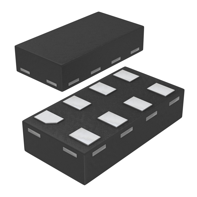
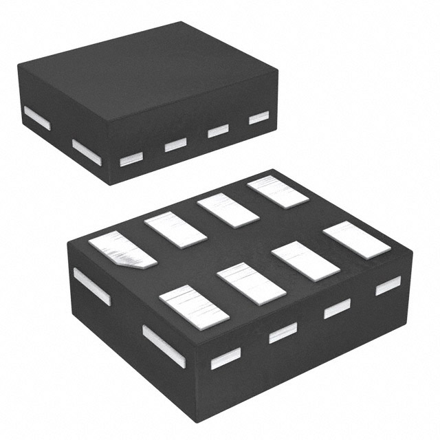
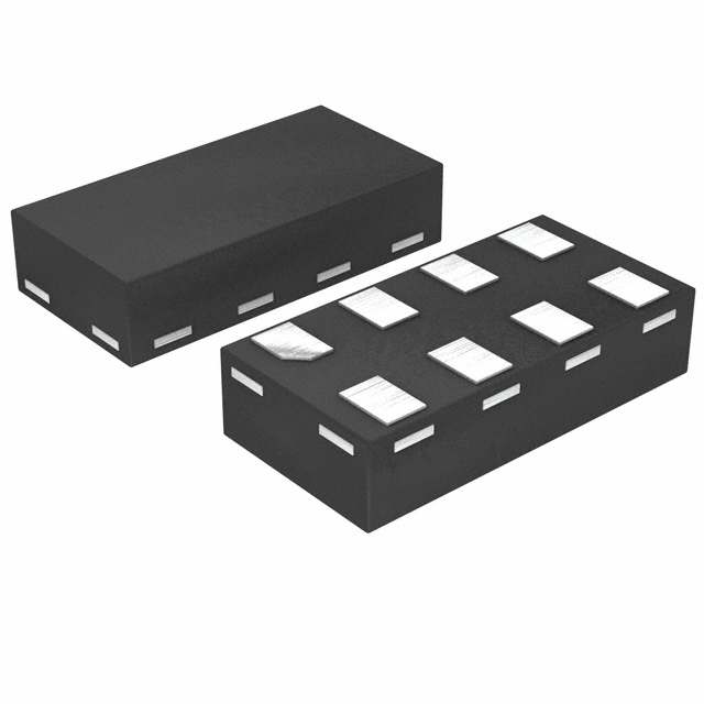
| Package / Case | 8-XFDFN |
| RoHS Status | ROHS3 Compliant |
| Moisture Sensitivity Level (MSL) | 1 (Unlimited) |
Substitute Part Grouping Explanation
Substitution eligibility for the 74LVC2G53GF,115 is determined by strict equivalence across the following critical parameters:
- Switch circuit type: SPDT
- Multiplexer/demultiplexer configuration: 2:1
- Number of circuits: 1
- On-state resistance: 10Ohm maximum
- Supply voltage range: 1.65V ~ 5.5V
- Switch timing: 3.8ns maximum (Ton, Toff)
- Bandwidth: 300MHz
- Charge injection: 7.5pC
- Channel capacitance: 6pF
- Leakage current: 5µA maximum
- Operating temperature: -40°C ~ 125°C
- Mounting type: Surface Mount
- Package family: 8-XFDFN
All substitute parts listed maintain these electrical and mechanical specifications. Variations in packaging dimensions (8-XSON form factors: 1.2x1, 1.35x1, 1.95x1) and supplier packaging formats (Bulk, Tape & Reel) do not affect functional equivalence. The base product numbers 74LVC2G53 and 74LVC1G53 are both acceptable within this substitution matrix.
Parameter Comparison
| Parameter | 74LVC2G53GF,115 | 74LVC2G53GS,115 | 74LVC1G53GN,115 | 74LVC1G53GS,115 | 74LVC1G53GT,115 | 74LVC2G53GN,115 | 74LVC2G53GT,115 |
|---|---|---|---|---|---|---|---|
| Manufacturer | Nexperia USA Inc. | NXP Semiconductors | Nexperia USA Inc. | NXP USA Inc. | Nexperia USA Inc. | Nexperia USA Inc. | NXP USA Inc. |
| Product Status | Obsolete | Active | Active | Active | Active | Active | Active |
| Switch Circuit | SPDT | SPDT | SPDT | SPDT | SPDT | SPDT | SPDT |
| Multiplexer Configuration | 2:1 | 2:1 | 2:1 | 2:1 | 2:1 | 2:1 | 2:1 |
| On-State Resistance (Max) | 10Ohm | 10Ohm | 10Ohm | 10Ohm | 10Ohm | 10Ohm | 10Ohm |
| Supply Voltage (V+) | 1.65V ~ 5.5V | 1.65V ~ 5.5V | 1.65V ~ 5.5V | 1.65V ~ 5.5V | 1.65V ~ 5.5V | 1.65V ~ 5.5V | 1.65V ~ 5.5V |
| Switch Time (Ton, Toff) Max | 3.8ns, 3.8ns | 3.8ns, 3.8ns | 3.8ns, 3.8ns | 3.8ns, 3.8ns | 3.8ns, 3.8ns | 3.8ns, 3.8ns | 3.8ns, 3.8ns |
| -3dB Bandwidth | 300MHz | 300MHz | 300MHz | 300MHz | 300MHz | 300MHz | 300MHz |
| Charge Injection | 7.5pC | 7.5pC | 7.5pC | 7.5pC | 7.5pC | 7.5pC | 7.5pC |
| Channel Capacitance (CS(off), CD(off)) | 6pF | 6pF | 6pF | 6pF | 6pF | 6pF | 6pF |
| Leakage Current (IS(off)) Max | 5µA | 5µA | 5µA | 5µA | 5µA | 5µA | 5µA |
| Operating Temperature | -40°C ~ 125°C | -40°C ~ 125°C | -40°C ~ 125°C | -40°C ~ 125°C | -40°C ~ 125°C | -40°C ~ 125°C | -40°C ~ 125°C |
| Package / Case | 8-XFDFN | 8-XFDFN | 8-XFDFN | 8-XFDFN | 8-XFDFN | 8-XFDFN | 8-XFDFN |
| Supplier Device Package | 8-XSON (1.35x1) | 8-XSON (1.35x1) | 8-XSON (1.2x1) | 8-XSON (1.35x1) | 8-XSON, SOT833-1 (1.95x1) | 8-XSON (1.2x1) | 8-XSON (1.95x1) |
| RoHS Status | ROHS3 Compliant | Not specified | ROHS3 Compliant | Not specified | ROHS3 Compliant | ROHS3 Compliant | Not specified |
| Moisture Sensitivity Level (MSL) | 1 (Unlimited) | Not specified | 1 (Unlimited) | Not specified | 1 (Unlimited) | 1 (Unlimited) | Not specified |
Engineering Selection Recommendations
All listed substitute parts maintain full electrical and functional equivalence to the 74LVC2G53GF,115. Selection among available substitutes should be based on:
Product Status: The 74LVC2G53GF,115 is obsolete. All substitute parts listed carry Active product status, ensuring long-term availability and manufacturing support.
Compliance and Certifications: Parts with documented ROHS3 compliance and MSL Level 1 rating (74LVC2G53GS,115, 74LVC1G53GN,115, 74LVC1G53GT,115, 74LVC2G53GN,115) provide explicit regulatory documentation. Parts without specified compliance information should be verified against your procurement requirements.
Packaging Format: Direct manufacturer equivalents (74LVC2G53GS,115, 74LVC2G53GN,115, 74LVC2G53GT,115) maintain the 74LVC2G53 base product number. Parametric equivalents using the 74LVC1G53 base product number (74LVC1G53GN,115, 74LVC1G53GS,115, 74LVC1G53GT,115) are functionally identical but use different base designations.
Supplier Packaging: Tape & Reel (TR) formats support automated assembly processes. Bulk packaging is suitable for manual assembly or lower-volume applications. Selection depends on manufacturing workflow requirements.
Physical Dimensions: All parts use 8-XSON form factors with variations in die size (1.2x1, 1.35x1, 1.95x1 mm). PCB layout compatibility should be verified against your design specifications.
Frequently Asked Questions (FAQ)
Q: Can I use 74LVC1G53 parts as direct replacements for 74LVC2G53GF,115?
A: Yes. The 74LVC1G53 variants (74LVC1G53GN,115, 74LVC1G53GS,115, 74LVC1G53GT,115) are parametric equivalents with identical electrical specifications. The base product number difference reflects internal die architecture but does not affect functional performance in this application.
Q: What is the difference between the packaging codes (GF, GS, GN, GT)?
A: The suffix codes indicate supplier packaging format and physical dimensions. GF and GS typically denote Bulk packaging; GN and GT denote Tape & Reel packaging. The numeric suffix (115) is a manufacturing code. All variants maintain the same electrical performance.
Q: Are there physical footprint differences between 8-XSON variants (1.2x1, 1.35x1, 1.95x1)?
A: Yes. The dimensions indicate die size variations within the 8-XFDFN package family. PCB land pattern compatibility must be verified. Consult the specific datasheet for your selected part number to confirm footprint alignment with your design.
Q: Why is the original 74LVC2G53GF,115 marked as obsolete?
A: Obsolescence reflects Nexperia's product lifecycle management. Active substitute parts with identical specifications are available from both Nexperia USA Inc. and NXP Semiconductors, ensuring design continuity without functional compromise.
Q: Do all substitute parts have the same RoHS and MSL certifications?
A: No. Parts with explicitly documented ROHS3 compliance and MSL Level 1 rating are: 74LVC2G53GS,115, 74LVC1G53GN,115, 74LVC1G53GT,115, and 74LVC2G53GN,115. Compliance information for other variants should be obtained from the manufacturer or distributor.
Q: Can I mix different substitute part numbers in the same design?
A: Yes, provided all selected parts meet your electrical, thermal, and compliance requirements. Mixing packaging formats (Bulk vs. Tape & Reel) is acceptable; however, verify that your assembly process supports the selected packaging types.
Alternative Parts

SJ6012L2TP
Littelfuse Inc.
6 Alternative Parts

JMK107BBJ476MA-RE
Taiyo Yuden
10 Alternative Parts

GMK107BBJ475MA-T
Taiyo Yuden
5 Alternative Parts
SJ6020N2ARP
Littelfuse Inc.
3 Alternative Parts
SJ6025R2ATP
Littelfuse Inc.
4 Alternative Parts

2474-05L
API Delevan Inc.
1 Alternative Parts

4590R-684K
API Delevan Inc.
1 Alternative Parts

CM6560R-334
API Delevan Inc.
1 Alternative Parts

CM6460-104
API Delevan Inc.
1 Alternative Parts

5526-12
API Delevan Inc.
1 Alternative Parts