


Request Quote
(Ships tomorrow)
74LVC2G08GS,115 Equivalent & Substitute Parts
Part Overview
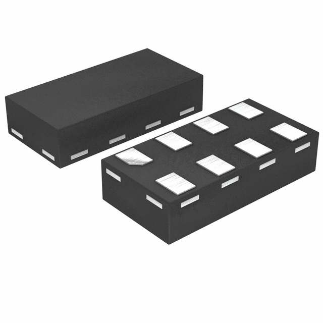
The 74LVC2G08GS,115 is a dual 2-input AND gate logic IC manufactured by Nexperia USA Inc. in the 74LVC series. This component is classified as an active product and is supplied in Tape & Reel (TR) packaging with an 8-XSON (1.35x1) footprint. The device integrates two independent AND gate circuits, each with two inputs, making it suitable for general-purpose logic applications requiring low-voltage operation and minimal power consumption. Equivalent and substitute parts are identified to provide design flexibility, accommodate supply chain variations, and support alternative packaging or sourcing requirements.
Substiute Parts
Key Parameters
| Parameter | Value |
|---|---|
| Logic Type | AND Gate |
| Number of Circuits | 2 |
| Number of Inputs | 2 |
| Voltage - Supply | 1.65V ~ 5.5V |
| Current - Quiescent (Max) | 4 µA |
| Current - Output High, Low | 32mA, 32mA |
| Input Logic Level - Low | 0.7V ~ 0.8V |
| Input Logic Level - High | 0.95V ~ 3.4V |
| Max Propagation Delay @ V, Max CL | 3.8ns @ 5V, 50pF |
| Operating Temperature | -40°C ~ 125°C (TA) |
| Mounting Type | Surface Mount |
| Package / Case | 8-XFDFN |
| Base Product Number | 74LVC2G08 |
| RoHS Status | ROHS3 Compliant |
| Moisture Sensitivity Level (MSL) | 1 (Unlimited) |
Substitute Part Grouping Explanation
Substitute parts for the 74LVC2G08GS,115 are identified based on strict parametric equivalence within the 74LVC2G08 base product family. All substitute candidates maintain identical electrical specifications across the following critical parameters:
- Logic function: Dual 2-input AND gate
- Supply voltage range: 1.65V ~ 5.5V
- Quiescent current: 4 µA maximum
- Output drive capability: 32mA high and low
- Input logic thresholds: 0.7V ~ 0.8V (low), 0.95V ~ 3.4V (high)
- Propagation delay: 3.8ns @ 5V, 50pF
- Operating temperature range: -40°C ~ 125°C
- Package type: 8-XFDFN
- Surface mount configuration
Substitution is permitted when packaging format (Tape & Reel vs. Bulk) and physical footprint dimensions are compatible with the application's assembly and PCB layout requirements. The 74LVC2G08GF,115 and 74LVC2G08GT,115 meet these criteria and are classified as parametric equivalents.
Parameter Comparison
| Parameter | 74LVC2G08GS,115 | 74LVC2G08GF,115 | 74LVC2G08GT,115 |
|---|---|---|---|
| Manufacturer | Nexperia USA Inc. | NXP USA Inc. | Nexperia USA Inc. |
| Logic Type | AND Gate | AND Gate | AND Gate |
| Number of Circuits | 2 | 2 | 2 |
| Number of Inputs | 2 | 2 | 2 |
| Voltage - Supply | 1.65V ~ 5.5V | 1.65V ~ 5.5V | 1.65V ~ 5.5V |
| Current - Quiescent (Max) | 4 µA | 4 µA | 4 µA |
| Current - Output High, Low | 32mA, 32mA | 32mA, 32mA | 32mA, 32mA |
| Input Logic Level - Low | 0.7V ~ 0.8V | 0.7V ~ 0.8V | 0.7V ~ 0.8V |
| Input Logic Level - High | 0.95V ~ 3.4V | 0.95V ~ 3.4V | 0.95V ~ 3.4V |
| Max Propagation Delay @ V, Max CL | 3.8ns @ 5V, 50pF | 3.8ns @ 5V, 50pF | 3.8ns @ 5V, 50pF |
| Operating Temperature | -40°C ~ 125°C (TA) | -40°C ~ 125°C (TA) | -40°C ~ 125°C (TA) |
| Mounting Type | Surface Mount | Surface Mount | Surface Mount |
| Supplier Device Package | 8-XSON (1.35x1) | 8-XSON (1.35x1) | 8-XSON, SOT833-1 (1.95x1) |
| Package / Case | 8-XFDFN | 8-XFDFN | 8-XFDFN |
| Base Product Number | 74LVC2G08 | 74LVC2G08 | 74LVC2G08 |
| Packaging Format | Tape & Reel (TR) | Bulk | Tape & Reel (TR) |
| Product Status | Active | Active | Active |
| RoHS Status | ROHS3 Compliant | Not specified | ROHS3 Compliant |
| Moisture Sensitivity Level (MSL) | 1 (Unlimited) | Not specified | 1 (Unlimited) |
Engineering Selection Recommendations
All three parts—74LVC2G08GS,115, 74LVC2G08GF,115, and 74LVC2G08GT,115—are active products with identical electrical performance and are suitable for direct substitution based on parametric equivalence.
The 74LVC2G08GS,115 and 74LVC2G08GT,115 are both supplied in Tape & Reel (TR) packaging and carry ROHS3 compliance certification with MSL Level 1 (Unlimited). These parts are preferred for high-volume automated assembly operations.
The 74LVC2G08GF,115 is supplied in Bulk packaging format and is suitable for applications where individual component handling or manual assembly is acceptable. This variant offers equivalent electrical performance but does not specify RoHS or MSL ratings in the provided data.
Physical footprint differences exist between the 74LVC2G08GS,115 (1.35x1) and 74LVC2G08GT,115 (1.95x1). PCB layout compatibility must be verified before substitution to ensure proper placement and soldering.
Frequently Asked Questions (FAQ)
Q: Can the 74LVC2G08GF,115 be used as a direct replacement for the 74LVC2G08GS,115?
A: Yes, from an electrical standpoint. Both parts share identical logic function, supply voltage range, output drive capability, and propagation delay specifications. The primary difference is packaging format: the GS variant is supplied in Tape & Reel, while the GF variant is supplied in Bulk. Selection depends on assembly process requirements and inventory management practices.
Q: What is the difference between the 74LVC2G08GS,115 and 74LVC2G08GT,115?
A: Both parts are supplied in Tape & Reel packaging and have identical electrical specifications. The key difference is physical footprint: the GS variant uses an 8-XSON (1.35x1) package, while the GT variant uses an 8-XSON, SOT833-1 (1.95x1) package. PCB layout and component placement must accommodate the larger footprint of the GT variant.
Q: Are all three parts RoHS compliant?
A: The 74LVC2G08GS,115 and 74LVC2G08GT,115 are explicitly ROHS3 compliant. The 74LVC2G08GF,115 does not specify RoHS status in the provided data. Compliance verification is required before use in applications with RoHS requirements.
Q: What is the Moisture Sensitivity Level (MSL) for these parts?
A: The 74LVC2G08GS,115 and 74LVC2G08GT,115 are rated MSL Level 1 (Unlimited), indicating no moisture sensitivity restrictions for storage or handling. The 74LVC2G08GF,115 does not specify MSL rating in the provided data.
Q: Can these parts operate at voltages below 1.65V or above 5.5V?
A: No. All three parts are specified for operation within the 1.65V to 5.5V supply voltage range. Operation outside this range is not supported and may result in device malfunction or damage.
Q: What is the maximum propagation delay for these AND gate ICs?
A: The maximum propagation delay is 3.8 nanoseconds at 5V supply voltage with a 50pF load capacitance. This specification is identical across all three substitute parts.
Alternative Parts

SJ6012L2TP
Littelfuse Inc.
6 Alternative Parts

JMK107BBJ476MA-RE
Taiyo Yuden
10 Alternative Parts

GMK107BBJ475MA-T
Taiyo Yuden
5 Alternative Parts
SJ6020N2ARP
Littelfuse Inc.
3 Alternative Parts
SJ6025R2ATP
Littelfuse Inc.
4 Alternative Parts

2474-05L
API Delevan Inc.
1 Alternative Parts

4590R-684K
API Delevan Inc.
1 Alternative Parts

CM6560R-334
API Delevan Inc.
1 Alternative Parts

CM6460-104
API Delevan Inc.
1 Alternative Parts

5526-12
API Delevan Inc.
1 Alternative Parts