


Request Quote
(Ships tomorrow)
74LVC273DB,112 Equivalent & Substitute Parts
Part Overview
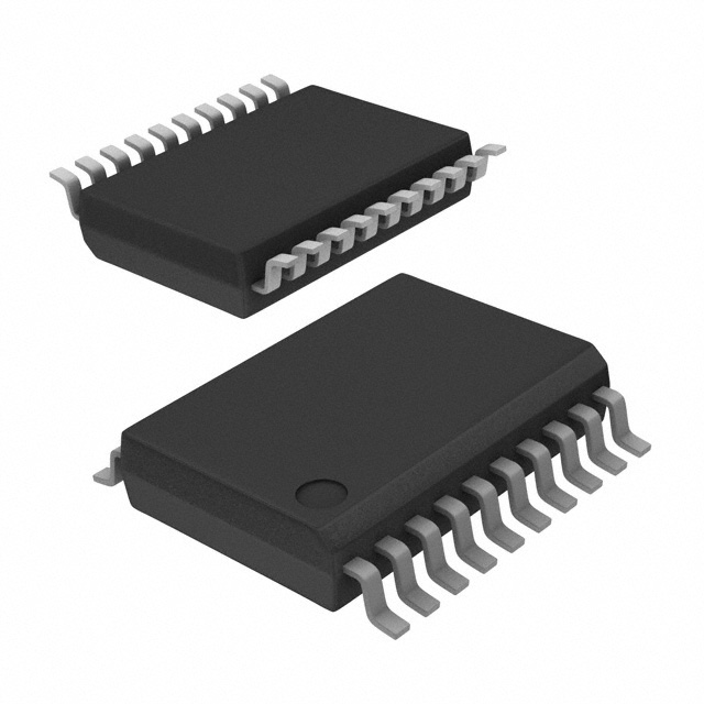
The 74LVC273DB,112 is a D-Type flip-flop logic integrated circuit manufactured by Nexperia USA Inc., designed for 8-bit parallel data storage and synchronous operation. This component features a master reset function, positive edge triggering, and operates across a 1.65V to 3.6V supply voltage range. The part is classified as obsolete, making identification of functionally equivalent alternatives essential for ongoing system support, design updates, and procurement continuity.
Substiute Parts
Key Parameters
| Parameter | Value |
|---|---|
| Manufacturer Part Number | 74LVC273DB,112 |
| Manufacturer | Nexperia USA Inc. |
| Category | Logic |
| Series | 74LVC |
| Function | Master Reset |
| Type | D-Type Flip Flop |
| Number of Elements | 1 |
| Number of Bits per Element | 8 |
| Output Type | Non-Inverted |
| Clock Frequency | 230 MHz |
| Trigger Type | Positive Edge |
| Voltage - Supply | 1.65V ~ 3.6V |
| Current - Output High, Low | 24mA, 24mA |
| Current - Quiescent (Iq) | 10 µA |
| Max Propagation Delay @ V, Max CL | 8.2ns @ 3.3V, 50pF |
| Input Capacitance | 5 pF |
| Operating Temperature | -40°C ~ 125°C (TA) |
| Package / Case | 20-SSOP (0.209", 5.30mm Width) |
| Mounting Type | Surface Mount |
| Product Status | Obsolete |
| RoHS Status | ROHS3 Compliant |
| Moisture Sensitivity Level (MSL) | 1 (Unlimited) |
Substitute Part Grouping Explanation
Substitute parts for the 74LVC273DB,112 are identified based on strict electrical and mechanical compatibility criteria. The following parameters determine valid substitution:
Critical Matching Parameters:
- Function: Master Reset
- Type: D-Type Flip Flop
- Number of Elements: 1
- Number of Bits per Element: 8
- Output Type: Non-Inverted
- Trigger Type: Positive Edge
- Operating Temperature Range: -40°C ~ 125°C (TA)
Acceptable Variation Parameters:
- Clock Frequency: Substitute must meet or exceed 230 MHz
- Voltage Supply Range: Substitute must support the 1.65V ~ 3.6V range or a compatible superset
- Current Output Ratings: Substitute must meet or exceed 24mA for both high and low outputs
- Propagation Delay: Substitute performance must be equal to or better than 8.2ns @ 3.3V, 50pF
- Package Type: Substitutes may differ in package form factor (SSOP vs. TSSOP) provided PCB layout accommodates the physical dimensions
Compliance Requirements:
- RoHS3 Compliant
- Moisture Sensitivity Level 1 (Unlimited)
Two substitute parts meet these criteria: 74LVC273PW,118 (Nexperia, same series, different package) and SN74LV273ADBR (Texas Instruments, related series with extended voltage range).
Parameter Comparison
| Parameter | 74LVC273DB,112 | 74LVC273PW,118 | SN74LV273ADBR |
|---|---|---|---|
| Manufacturer | Nexperia USA Inc. | Nexperia USA Inc. | Texas Instruments |
| Series | 74LVC | 74LVC | 74LV |
| Function | Master Reset | Master Reset | Master Reset |
| Type | D-Type | D-Type | D-Type |
| Number of Elements | 1 | 1 | 1 |
| Number of Bits per Element | 8 | 8 | 8 |
| Output Type | Non-Inverted | Non-Inverted | Non-Inverted |
| Clock Frequency | 230 MHz | 230 MHz | 205 MHz |
| Trigger Type | Positive Edge | Positive Edge | Positive Edge |
| Voltage - Supply | 1.65V ~ 3.6V | 1.65V ~ 3.6V | 2V ~ 5.5V |
| Current - Output High, Low | 24mA, 24mA | 24mA, 24mA | 12mA, 12mA |
| Current - Quiescent (Iq) | 10 µA | 10 µA | 20 µA |
| Max Propagation Delay @ V, Max CL | 8.2ns @ 3.3V, 50pF | 8.2ns @ 3.3V, 50pF | 6.2ns @ 5V, 50pF |
| Input Capacitance | 5 pF | 5 pF | 2 pF |
| Operating Temperature | -40°C ~ 125°C (TA) | -40°C ~ 125°C (TA) | -40°C ~ 125°C (TA) |
| Package / Case | 20-SSOP (0.209", 5.30mm Width) | 20-TSSOP (0.173", 4.40mm Width) | 20-SSOP (0.209", 5.30mm Width) |
| Mounting Type | Surface Mount | Surface Mount | Surface Mount |
| Product Status | Obsolete | Active | Active |
| RoHS Status | ROHS3 Compliant | ROHS3 Compliant | ROHS3 Compliant |
| Moisture Sensitivity Level (MSL) | 1 (Unlimited) | 1 (Unlimited) | 1 (Unlimited) |
Engineering Selection Recommendations
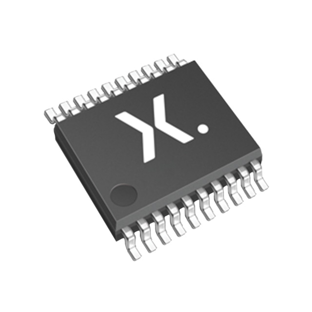
74LVC273PW,118 (Nexperia USA Inc.)
This substitute maintains identical electrical specifications to the 74LVC273DB,112 while offering active product status. Both parts belong to the 74LVC series and share the same supply voltage range (1.65V ~ 3.6V), clock frequency (230 MHz), output current ratings (24mA), and propagation delay characteristics (8.2ns @ 3.3V, 50pF). The primary difference is the package form factor: 20-TSSOP (0.173", 4.40mm Width) versus 20-SSOP (0.209", 5.30mm Width). This substitute is suitable for new designs or redesigns where PCB layout can accommodate the narrower TSSOP package. Both parts maintain ROHS3 compliance and MSL 1 rating.
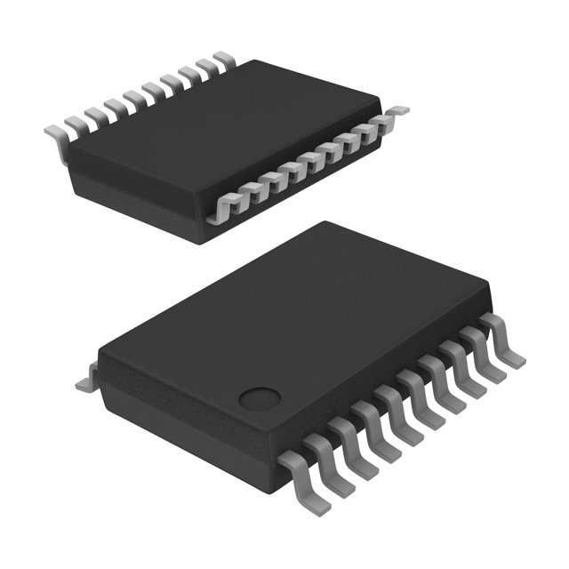
SN74LV273ADBR (Texas Instruments)
This substitute provides functional equivalence with extended voltage supply range (2V ~ 5.5V) compared to the original part (1.65V ~ 3.6V). The SN74LV273ADBR maintains the same package form factor (20-SSOP, 0.209", 5.30mm Width) as the 74LVC273DB,112, enabling direct PCB compatibility. However, this part exhibits reduced output current ratings (12mA versus 24mA) and higher quiescent current (20 µA versus 10 µA). Clock frequency is slightly lower at 205 MHz versus 230 MHz. This substitute is appropriate for applications where the extended voltage range is beneficial and output current requirements do not exceed 12mA. Both parts maintain ROHS3 compliance and MSL 1 rating.
Frequently Asked Questions (FAQ)
Q: Can the 74LVC273PW,118 be used as a direct replacement for the 74LVC273DB,112 on existing PCBs?
A: The 74LVC273PW,118 is electrically equivalent but uses a different package form factor (20-TSSOP versus 20-SSOP). Direct PCB replacement is not possible without layout modification. The TSSOP package is narrower (0.173" versus 0.209" width), requiring PCB footprint adjustment. For new designs or PCB revisions, this substitute is suitable.
Q: What are the key differences between the 74LVC273DB,112 and SN74LV273ADBR?
A: Both parts share identical package form factor (20-SSOP) and core D-Type flip-flop functionality. The SN74LV273ADBR offers extended voltage supply range (2V ~ 5.5V versus 1.65V ~ 3.6V) but with reduced output current capacity (12mA versus 24mA), higher quiescent current (20 µA versus 10 µA), and slightly lower clock frequency (205 MHz versus 230 MHz). Selection depends on application voltage requirements and output current demands.
Q: Are both substitute parts RoHS compliant?
A: Yes. Both 74LVC273PW,118 and SN74LV273ADBR are ROHS3 compliant with Moisture Sensitivity Level 1 (Unlimited), matching the compliance profile of the 74LVC273DB,112.
Q: Why is the 74LVC273DB,112 marked as obsolete?
A: The 74LVC273DB,112 is classified as obsolete by the manufacturer. The 74LVC273PW,118 (same series, active status) and SN74LV273ADBR (related series, active status) represent current production alternatives that maintain functional and electrical compatibility.
Q: Which substitute should I select for a new design?
A: For new designs requiring identical electrical performance and the same package footprint, select the SN74LV273ADBR. For designs where package size optimization is a priority and PCB layout can accommodate the narrower TSSOP form factor, select the 74LVC273PW,118. Both parts are in active production status.
Q: Can the SN74LV273ADBR handle the same output current as the original part?
A: No. The SN74LV273ADBR provides 12mA output current (both high and low) compared to 24mA for the 74LVC273DB,112. Applications requiring output currents exceeding 12mA must use the 74LVC273PW,118 or implement external buffering with the SN74LV273ADBR.
Alternative Parts

SJ6012L2TP
Littelfuse Inc.
6 Alternative Parts

JMK107BBJ476MA-RE
Taiyo Yuden
10 Alternative Parts

GMK107BBJ475MA-T
Taiyo Yuden
5 Alternative Parts
SJ6020N2ARP
Littelfuse Inc.
3 Alternative Parts
SJ6025R2ATP
Littelfuse Inc.
4 Alternative Parts

2474-05L
API Delevan Inc.
1 Alternative Parts

4590R-684K
API Delevan Inc.
1 Alternative Parts

CM6560R-334
API Delevan Inc.
1 Alternative Parts

CM6460-104
API Delevan Inc.
1 Alternative Parts

5526-12
API Delevan Inc.
1 Alternative Parts