


Request Quote
(Ships tomorrow)
74LVC11DB,112 Equivalent & Substitute Parts
Part Overview
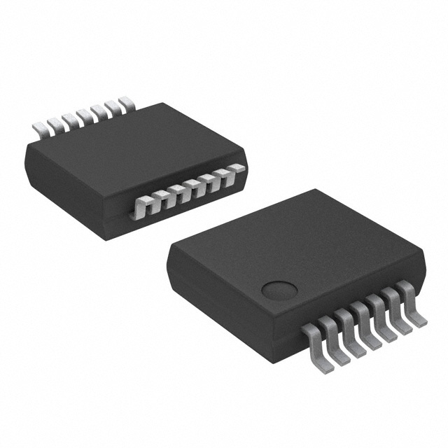
The 74LVC11DB,112 is a 3-channel AND gate logic IC manufactured by Nexperia USA Inc., housed in a 14-SSOP surface mount package. This component is classified as obsolete, making equivalent and substitute parts necessary for new designs and production continuity. The part operates across a supply voltage range of 1.2V to 3.6V with low quiescent current and standard propagation delay characteristics suitable for general-purpose logic applications.
Substiute Parts
Key Parameters
| Parameter | Value |
|---|---|
| Logic Type | AND Gate |
| Number of Circuits | 3 |
| Number of Inputs | 3 |
| Voltage - Supply | 1.2V ~ 3.6V |
| Current - Quiescent (Max) | 10 µA |
| Current - Output High, Low | 24mA, 24mA |
| Max Propagation Delay @ V, Max CL | 6.2ns @ 3.3V, 50pF |
| Operating Temperature | -40°C ~ 125°C |
| Mounting Type | Surface Mount |
| Package / Case | 14-SSOP (0.209", 5.30mm Width) |
| Product Status | Obsolete |
Substitute Part Grouping Explanation
Substitute parts for the 74LVC11DB,112 are selected based on functional equivalence as 3-channel, 3-input AND gate logic ICs with compatible electrical characteristics. The primary substitution criteria are:
- Logic function: 3-channel AND gate with 3 inputs per channel
- Supply voltage compatibility: Parts must operate within overlapping voltage ranges
- Output drive capability: 24mA output current maintained across substitutes
- Propagation delay: Performance within acceptable timing parameters
- Package compatibility: Surface mount packages suitable for 14-pin configurations
- Product status: Active parts preferred for design continuity
The 74LCX11MTCX and SN74AC11DBR meet these criteria with functional equivalence, though with variations in voltage range, quiescent current, and operating temperature limits.
Parameter Comparison
| Parameter | 74LVC11DB,112 | 74LCX11MTCX | SN74AC11DBR |
|---|---|---|---|
| Manufacturer | Nexperia USA Inc. | Fairchild Semiconductor | Texas Instruments |
| Logic Type | AND Gate | AND Gate | AND Gate |
| Number of Circuits | 3 | 3 | 3 |
| Number of Inputs | 3 | 3 | 3 |
| Voltage - Supply | 1.2V ~ 3.6V | 2V ~ 3.6V | 2V ~ 6V |
| Current - Quiescent (Max) | 10 µA | 10 µA | 2 µA |
| Current - Output High, Low | 24mA, 24mA | 24mA, 24mA | 24mA, 24mA |
| Input Logic Level - Low | 0.12V ~ 0.8V | 0.7V ~ 0.8V | 0.9V ~ 1.65V |
| Input Logic Level - High | 1.08V ~ 2V | 1.7V ~ 2V | 2.1V ~ 3.85V |
| Max Propagation Delay @ V, Max CL | 6.2ns @ 3.3V, 50pF | 6ns @ 3.3V, 50pF | 8ns @ 5V, 50pF |
| Operating Temperature | -40°C ~ 125°C | -40°C ~ 85°C | -40°C ~ 85°C |
| Mounting Type | Surface Mount | Surface Mount | Surface Mount |
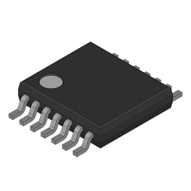
| Package / Case | 14-SSOP (0.209", 5.30mm Width) | 14-TSSOP (0.173", 4.40mm Width) | 14-SSOP (0.209", 5.30mm Width) |
| Product Status | Obsolete | Active | Active |
| RoHS Status | ROHS3 Compliant | Not specified | ROHS3 Compliant |
Engineering Selection Recommendations
SN74AC11DBR (Texas Instruments) is the primary substitute for the 74LVC11DB,112. This part maintains identical package geometry (14-SSOP), matching PCB layout requirements without redesign. The SN74AC11DBR is active in production with ROHS3 compliance certification. The extended supply voltage range (2V ~ 6V) provides broader application flexibility compared to the original part. Quiescent current is reduced to 2 µA, offering improved power efficiency. The operating temperature range is limited to -40°C ~ 85°C, which is acceptable for most commercial and industrial applications.
74LCX11MTCX (Fairchild Semiconductor) serves as an alternative substitute with active product status. This part maintains functional equivalence with matching quiescent current (10 µA) and propagation delay (6ns @ 3.3V, 50pF). However, the 14-TSSOP package has a reduced width (4.40mm versus 5.30mm), requiring PCB layout verification and potential footprint adjustment. The supply voltage range (2V ~ 3.6V) is narrower than the original part, limiting low-voltage applications below 2V.
For designs requiring the original 1.2V minimum supply voltage, neither substitute fully maintains this specification. The SN74AC11DBR minimum of 2V represents the closest available alternative with active production status and compliance certification.
Frequently Asked Questions (FAQ)
Q: Can the SN74AC11DBR directly replace the 74LVC11DB,112 without PCB modifications?
A: Yes. Both parts use the 14-SSOP package with identical 0.209" width and 5.30mm dimensions, allowing direct footprint compatibility without PCB layout changes.
Q: What is the key difference between the 74LCX11MTCX and SN74AC11DBR substitutes?
A: The 74LCX11MTCX uses a 14-TSSOP package (4.40mm width) requiring footprint verification, while the SN74AC11DBR maintains the original 14-SSOP package (5.30mm width). The SN74AC11DBR offers lower quiescent current (2 µA versus 10 µA) and extended supply voltage range (2V ~ 6V versus 2V ~ 3.6V).
Q: Is the reduced operating temperature range of the substitutes acceptable?
A: The SN74AC11DBR and 74LCX11MTCX both support -40°C ~ 85°C, which covers standard commercial and industrial temperature ranges. Applications requiring operation above 85°C cannot use these substitutes.
Q: Why does the 74LVC11DB,112 show as obsolete?
A: The original part is no longer in active production. The SN74AC11DBR and 74LCX11MTCX are active alternatives that provide equivalent logic functionality for new designs and production continuity.
Q: Are both substitutes RoHS compliant?
A: The SN74AC11DBR carries ROHS3 compliance certification. RoHS status for the 74LCX11MTCX is not specified in the available data.
Q: What is the minimum supply voltage for each part?
A: The original 74LVC11DB,112 operates at 1.2V minimum. The SN74AC11DBR and 74LCX11MTCX both require 2V minimum, limiting use in ultra-low-voltage applications below 2V.
Alternative Parts

SJ6012L2TP
Littelfuse Inc.
6 Alternative Parts

JMK107BBJ476MA-RE
Taiyo Yuden
10 Alternative Parts

GMK107BBJ475MA-T
Taiyo Yuden
5 Alternative Parts
SJ6020N2ARP
Littelfuse Inc.
3 Alternative Parts
SJ6025R2ATP
Littelfuse Inc.
4 Alternative Parts

2474-05L
API Delevan Inc.
1 Alternative Parts

4590R-684K
API Delevan Inc.
1 Alternative Parts

CM6560R-334
API Delevan Inc.
1 Alternative Parts

CM6460-104
API Delevan Inc.
1 Alternative Parts

5526-12
API Delevan Inc.
1 Alternative Parts