


Request Quote
(Ships tomorrow)
74LVC109DB,112 Equivalent & Substitute Parts
Part Overview
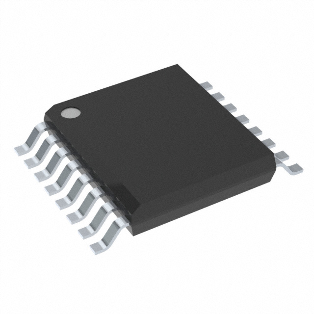
The 74LVC109DB,112 is a dual JK-type flip-flop logic integrated circuit manufactured by NXP USA Inc., housed in a 16-SSOP surface mount package. This component functions as a Set(Preset) and Reset element with complementary outputs, operating across a supply voltage range of 1.65V to 3.6V. The device is classified as obsolete, making identification of functionally equivalent alternatives necessary for ongoing design support and production continuity.
Substiute Parts
Key Parameters
| Parameter | Value |
|---|---|
| Manufacturer Part Number | 74LVC109DB,112 |
| Manufacturer | NXP USA Inc. |
| Category | Logic |
| Series | 74LVC |
| Type | JK Type Flip-Flop |
| Number of Elements | 2 |
| Number of Bits per Element | 1 |
| Output Type | Complementary |
| Package / Case | 16-SSOP (0.209", 5.30mm Width) |
| Mounting Type | Surface Mount |
| Voltage - Supply | 1.65V ~ 3.6V |
| Operating Temperature | -40°C ~ 125°C (TA) |
| Product Status | Obsolete |
| RoHS Status | ROHS3 Compliant |
| Moisture Sensitivity Level (MSL) | 1 (Unlimited) |
Substitute Part Grouping Explanation
Substitution of the 74LVC109DB,112 is determined by the following critical parameters:
- Logic Family & Function: Both parts belong to the 74LVC series and implement dual JK-type flip-flops with complementary outputs and Set(Preset)/Reset functionality
- Package Compatibility: Identical 16-SSOP surface mount package (0.209", 5.30mm Width) ensures mechanical and electrical pin compatibility
- Supply Voltage Range: Both parts operate within 1.65V to 3.6V, maintaining voltage compatibility across applications
- Output Drive Capability: Matching output current specifications (24mA high, 24mA low) ensure equivalent load-driving performance
- Quiescent Current: Identical 10 µA specification maintains power consumption characteristics
- Compliance & Certifications: Both parts meet ROHS3, REACH Unaffected, and MSL 1 requirements
The primary technical difference is the trigger type: the 74LVC109DB,112 uses positive edge triggering, while the SN74LVC112ADBR uses negative edge triggering. This distinction is fundamental to circuit operation and must be evaluated against specific application requirements.
Parameter Comparison
| Parameter | 74LVC109DB,112 (NXP) | SN74LVC112ADBR (Texas Instruments) |
|---|---|---|
| Manufacturer | NXP USA Inc. | Texas Instruments |
| Product Status | Obsolete | Active |
| Type | JK Type Flip-Flop | JK Type Flip-Flop |
| Number of Elements | 2 | 2 |
| Number of Bits per Element | 1 | 1 |
| Output Type | Complementary | Complementary |
| Trigger Type | Positive Edge | Negative Edge |
| Clock Frequency | 330 MHz | 150 MHz |
| Max Propagation Delay @ 3.3V, 50pF | 6.8ns | 5.9ns |
| Current - Output High, Low | 24mA, 24mA | 24mA, 24mA |
| Voltage - Supply | 1.65V ~ 3.6V | 1.65V ~ 3.6V |
| Current - Quiescent (Iq) | 10 µA | 10 µA |
| Input Capacitance | 5 pF | 4.5 pF |
| Operating Temperature | -40°C ~ 125°C | -40°C ~ 85°C |
| Package / Case | 16-SSOP (0.209", 5.30mm Width) | 16-SSOP (0.209", 5.30mm Width) |
| Mounting Type | Surface Mount | Surface Mount |
| RoHS Status | ROHS3 Compliant | ROHS3 Compliant |
| Moisture Sensitivity Level (MSL) | 1 (Unlimited) | 1 (Unlimited) |
Engineering Selection Recommendations
The SN74LVC112ADBR from Texas Instruments is available as an active product with full manufacturing support, addressing the obsolescence status of the 74LVC109DB,112. Both parts maintain ROHS3 compliance and MSL 1 certification, ensuring regulatory and environmental compatibility.
Selection between these parts depends on trigger polarity requirements. The 74LVC109DB,112 operates on positive edge triggering, while the SN74LVC112ADBR operates on negative edge triggering. This functional difference requires circuit-level evaluation to determine compatibility with existing clock signal conditioning.
The SN74LVC112ADBR demonstrates superior propagation delay performance (5.9ns versus 6.8ns at 3.3V, 50pF load) and lower input capacitance (4.5pF versus 5pF), providing marginal timing advantages. The 74LVC109DB,112 supports higher clock frequency operation (330 MHz versus 150 MHz) and extended operating temperature range (-40°C to 125°C versus -40°C to 85°C).
Frequently Asked Questions (FAQ)
Q: Can the SN74LVC112ADBR directly replace the 74LVC109DB,112 without circuit modification?
A: Direct pin-for-pin replacement is possible due to identical 16-SSOP packaging. However, the trigger polarity difference (negative edge versus positive edge) requires verification that clock signals and circuit timing logic accommodate this functional change.
Q: Are there package compatibility concerns between these parts?
A: No. Both parts use the 16-SSOP (0.209", 5.30mm Width) surface mount package with identical pinout and mechanical dimensions, ensuring PCB footprint compatibility.
Q: What are the voltage supply compatibility considerations?
A: Both parts operate within the identical 1.65V to 3.6V supply range, maintaining full voltage compatibility across standard logic supply levels (3.3V, 2.5V, 1.8V).
Q: How do the operating temperature ranges compare?
A: The 74LVC109DB,112 supports -40°C to 125°C operation, while the SN74LVC112ADBR supports -40°C to 85°C. Applications requiring extended high-temperature operation above 85°C must retain the original part or identify alternative solutions.
Q: Are there compliance or certification differences?
A: Both parts meet identical compliance requirements: ROHS3 Compliant, REACH Unaffected, MSL 1 (Unlimited), and EAR99 classification. No regulatory barriers exist to substitution.
Q: What is the significance of the clock frequency difference?
A: The 74LVC109DB,112 supports 330 MHz operation versus 150 MHz for the SN74LVC112ADBR. Applications operating above 150 MHz require the original part or alternative high-speed logic devices.
Alternative Parts

SJ6012L2TP
Littelfuse Inc.
6 Alternative Parts

JMK107BBJ476MA-RE
Taiyo Yuden
10 Alternative Parts

GMK107BBJ475MA-T
Taiyo Yuden
5 Alternative Parts
SJ6020N2ARP
Littelfuse Inc.
3 Alternative Parts
SJ6025R2ATP
Littelfuse Inc.
4 Alternative Parts

2474-05L
API Delevan Inc.
1 Alternative Parts

4590R-684K
API Delevan Inc.
1 Alternative Parts

CM6560R-334
API Delevan Inc.
1 Alternative Parts

CM6460-104
API Delevan Inc.
1 Alternative Parts

5526-12
API Delevan Inc.
1 Alternative Parts