


Request Quote
(Ships tomorrow)
74LVC109D,112 Equivalent & Substitute Parts
Part Overview
The 74LVC109D,112 is a dual JK-type flip-flop logic integrated circuit manufactured by NXP USA Inc., designed for digital logic applications requiring edge-triggered state control. This device features complementary outputs and operates across a wide supply voltage range of 1.65V to 3.6V, making it suitable for low-voltage digital systems.
The 74LVC109D,112 is classified as obsolete, which necessitates identification of active equivalent parts for new designs and ongoing production requirements. The substitute part SN74LVC112AD from Texas Instruments provides functional compatibility while maintaining active product status and full component availability.
Substiute Parts
Key Parameters
| Parameter | Value |
|---|---|
| Manufacturer Part Number | 74LVC109D,112 |
| Manufacturer | NXP USA Inc. |
| Category | Logic |
| Type | JK Type Flip-Flop |
| Number of Elements | 2 |
| Number of Bits per Element | 1 |
| Output Type | Complementary |
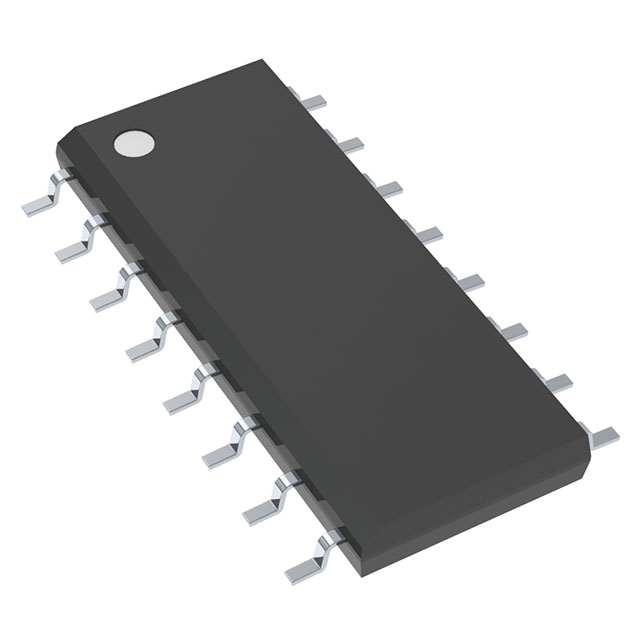
| Package / Case | 16-SOIC (0.154", 3.90mm Width) |
| Voltage - Supply | 1.65V ~ 3.6V |
| Operating Temperature | -40°C ~ 125°C (TA) |
| Mounting Type | Surface Mount |
| Product Status | Obsolete |
| RoHS Status | ROHS3 Compliant |
Substitute Part Grouping Explanation
Substitution of the 74LVC109D,112 is determined by the following critical parameters:
Mechanical Compatibility:
- Package type: 16-SOIC (0.154", 3.90mm Width)
- Mounting type: Surface Mount
- Pin count and footprint alignment
Electrical Compatibility:
- Supply voltage range: 1.65V ~ 3.6V
- Output type: Complementary
- Function: Set(Preset) and Reset capability
- Number of elements: 2
- Bits per element: 1
Functional Compatibility:
- Logic family: 74LVC series
- Device type: JK-type flip-flop
- Output drive capability: 24mA (High and Low)
- Quiescent current: 10 µA
The SN74LVC112AD from Texas Instruments meets all mechanical and electrical compatibility requirements. The primary functional difference is the trigger type: the 74LVC109D,112 uses positive edge triggering, while the SN74LVC112AD uses negative edge triggering. This difference requires circuit-level evaluation based on the specific application's clock signal polarity requirements.
Parameter Comparison
| Parameter | 74LVC109D,112 (NXP) | SN74LVC112AD (Texas Instruments) |
|---|---|---|
| Manufacturer | NXP USA Inc. | Texas Instruments |
| Product Status | Obsolete | Active |
| Type | JK Type | JK Type |
| Number of Elements | 2 | 2 |
| Number of Bits per Element | 1 | 1 |
| Output Type | Complementary | Complementary |
| Trigger Type | Positive Edge | Negative Edge |
| Clock Frequency | 330 MHz | 150 MHz |
| Max Propagation Delay @ 3.3V, 50pF | 6.8ns | 5.9ns |
| Current - Output High, Low | 24mA, 24mA | 24mA, 24mA |
| Voltage - Supply | 1.65V ~ 3.6V | 1.65V ~ 3.6V |
| Current - Quiescent (Iq) | 10 µA | 10 µA |
| Input Capacitance | 5 pF | 4.5 pF |
| Operating Temperature | -40°C ~ 125°C | -40°C ~ 85°C |
| Package / Case | 16-SOIC (0.154", 3.90mm Width) | 16-SOIC (0.154", 3.90mm Width) |
| Mounting Type | Surface Mount | Surface Mount |
| RoHS Status | ROHS3 Compliant | ROHS3 Compliant |
| Moisture Sensitivity Level (MSL) | 1 (Unlimited) | 1 (Unlimited) |
Engineering Selection Recommendations
The SN74LVC112AD is the direct active substitute for the obsolete 74LVC109D,112. Both devices are ROHS3 compliant and REACH unaffected, meeting current regulatory requirements for electronic component manufacturing and use.
Selection of the SN74LVC112AD is appropriate for applications where:
- The circuit design accommodates negative edge triggering instead of positive edge triggering
- Operating temperature requirements do not exceed 85°C (the SN74LVC112AD upper limit is 85°C versus 125°C for the 74LVC109D,112)
- Clock frequency requirements are within 150 MHz specification
The SN74LVC112AD offers superior propagation delay performance (5.9ns versus 6.8ns) and lower input capacitance (4.5 pF versus 5 pF), providing marginal performance advantages in timing-critical applications.
Frequently Asked Questions (FAQ)
Q: Can the SN74LVC112AD be used as a direct pin-for-pin replacement for the 74LVC109D,112?
A: The SN74LVC112AD shares identical pinout and 16-SOIC package dimensions with the 74LVC109D,112. However, the trigger type differs: the 74LVC109D,112 triggers on positive clock edges, while the SN74LVC112AD triggers on negative clock edges. Direct substitution requires circuit-level verification that the clock signal polarity is compatible with negative edge triggering.
Q: What is the primary difference between these two devices?
A: The primary functional difference is the clock trigger polarity. The 74LVC109D,112 uses positive edge triggering, while the SN74LVC112AD uses negative edge triggering. Secondary differences include maximum clock frequency (330 MHz versus 150 MHz) and maximum operating temperature (125°C versus 85°C).
Q: Are both devices compatible with the same supply voltage range?
A: Yes. Both the 74LVC109D,112 and SN74LVC112AD operate across the identical supply voltage range of 1.65V to 3.6V, ensuring compatibility in low-voltage digital systems.
Q: What are the compliance and regulatory considerations?
A: Both devices are ROHS3 compliant and REACH unaffected, meeting current environmental and regulatory standards for electronic components. Both devices carry Moisture Sensitivity Level 1 (Unlimited), indicating no moisture sensitivity restrictions during storage and handling.
Q: Does the SN74LVC112AD meet the operating temperature requirements of the original design?
A: The SN74LVC112AD operates from -40°C to 85°C, while the 74LVC109D,112 operates from -40°C to 125°C. Applications requiring operation above 85°C require alternative solutions, as the SN74LVC112AD does not meet the extended temperature specification.
Alternative Parts

SJ6012L2TP
Littelfuse Inc.
6 Alternative Parts

JMK107BBJ476MA-RE
Taiyo Yuden
10 Alternative Parts

GMK107BBJ475MA-T
Taiyo Yuden
5 Alternative Parts
SJ6020N2ARP
Littelfuse Inc.
3 Alternative Parts
SJ6025R2ATP
Littelfuse Inc.
4 Alternative Parts

2474-05L
API Delevan Inc.
1 Alternative Parts

4590R-684K
API Delevan Inc.
1 Alternative Parts

CM6560R-334
API Delevan Inc.
1 Alternative Parts

CM6460-104
API Delevan Inc.
1 Alternative Parts

5526-12
API Delevan Inc.
1 Alternative Parts