


Request Quote
(Ships tomorrow)
74LVC06ADTR2G Equivalent & Substitute Parts
Part Overview
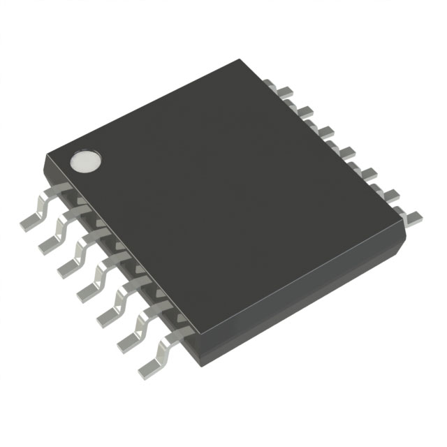
The 74LVC06ADTR2G is a 6-channel inverter IC with open drain output configuration, manufactured by onsemi in a 14-TSSOP surface mount package. This device is classified as obsolete, making identification of functionally equivalent alternatives essential for ongoing design support and production continuity. The part operates across a wide supply voltage range of 1.2V to 5.5V with a maximum propagation delay of 6ns at 5V with 50pF load.
Substiute Parts
Key Parameters
| Parameter | Value |
|---|---|
| Logic Type | Inverter |
| Number of Circuits | 6 |
| Number of Inputs | 1 |
| Features | Open Drain |
| Voltage - Supply | 1.2V ~ 5.5V |
| Current - Quiescent (Max) | 40 µA |
| Current - Output High, Low | -, 32mA |
| Max Propagation Delay @ V, Max CL | 6ns @ 5V, 50pF |
| Operating Temperature | -40°C ~ 125°C |
| Package / Case | 14-TSSOP (0.173", 4.40mm Width) |
| Product Status | Obsolete |
Substitute Part Grouping Explanation
Substitution of the 74LVC06ADTR2G is determined by the following critical parameters:
- Logic Configuration: 6-channel inverter with open drain output
- Package Type: 14-TSSOP surface mount package with identical physical dimensions
- Functional Equivalence: Single input per channel, inverting logic
- Supply Voltage Compatibility: Operating voltage range must support the application requirements
- Output Drive Capability: Open drain output current rating must meet load requirements
The MC74LCX06DTR2G qualifies as a direct substitute based on matching logic configuration, package type, and functional architecture. Both devices implement identical 6-channel inverter topology with open drain outputs in the same 14-TSSOP package footprint.
Parameter Comparison
| Parameter | 74LVC06ADTR2G | MC74LCX06DTR2G | Compatibility Notes |
|---|---|---|---|
| Logic Type | Inverter | Inverter | Identical |
| Number of Circuits | 6 | 6 | Identical |
| Number of Inputs | 1 | 1 | Identical |
| Features | Open Drain | Open Drain | Identical |
| Voltage - Supply | 1.2V ~ 5.5V | 2V ~ 3.6V | MC74LCX06DTR2G operates within narrower range; suitable for 2V to 3.6V applications |
| Current - Quiescent (Max) | 40 µA | 10 µA | MC74LCX06DTR2G has lower quiescent current |
| Current - Output High, Low | -, 32mA | -, 24mA | MC74LCX06DTR2G has reduced output current; verify load requirements |
| Max Propagation Delay @ V, Max CL | 6ns @ 5V, 50pF | 3.7ns @ 3.3V, 50pF | MC74LCX06DTR2G has faster propagation delay at 3.3V |
| Operating Temperature | -40°C ~ 125°C | -40°C ~ 85°C | 74LVC06ADTR2G supports extended high temperature operation |
| Package / Case | 14-TSSOP (0.173", 4.40mm Width) | 14-TSSOP (0.173", 4.40mm Width) | Identical footprint and pinout |
| Product Status | Obsolete | Active | MC74LCX06DTR2G is actively manufactured |
| RoHS Status | ROHS3 Compliant | ROHS3 Compliant | Both meet RoHS3 requirements |
Engineering Selection Recommendations
The MC74LCX06DTR2G is the qualified substitute for the obsolete 74LVC06ADTR2G based on the following criteria:
Functional Compatibility: Both devices implement identical 6-channel inverter logic with open drain outputs in the same 14-TSSOP package, ensuring direct pinout compatibility and footprint equivalence.
Regulatory Compliance: Both parts maintain ROHS3 compliance and REACH unaffected status, meeting current environmental and regulatory requirements.
Operational Constraints: Selection of MC74LCX06DTR2G requires verification of three parameters within the application:
- Supply voltage must remain within the 2V to 3.6V range
- Output current requirements must not exceed 24mA per channel
- Operating temperature must not exceed 85°C
Applications requiring supply voltages below 2V or above 3.6V, output currents exceeding 24mA, or operating temperatures above 85°C cannot use the MC74LCX06DTR2G as a direct substitute.
Frequently Asked Questions (FAQ)
Q: Can MC74LCX06DTR2G replace 74LVC06ADTR2G in all applications?
A: No. The MC74LCX06DTR2G operates within a narrower supply voltage range (2V to 3.6V versus 1.2V to 5.5V), has reduced output current capability (24mA versus 32mA), and supports a lower maximum operating temperature (85°C versus 125°C). Substitution is valid only when all three parameters fall within the MC74LCX06DTR2G specifications.
Q: Are the packages physically identical?
A: Yes. Both devices use the 14-TSSOP package with identical footprint dimensions (0.173" width, 4.40mm). PCB layout and component placement require no modification.
Q: What is the pinout compatibility?
A: Both devices maintain identical pinout configuration as 6-channel inverters with open drain outputs. No pin reassignment or board redesign is necessary.
Q: Why does MC74LCX06DTR2G have lower quiescent current?
A: The MC74LCX06DTR2G is optimized for lower voltage operation (2V to 3.6V), resulting in reduced quiescent current consumption (10 µA versus 40 µA). This characteristic is inherent to the device design and does not affect functional equivalence.
Q: Is the propagation delay difference significant?
A: The MC74LCX06DTR2G exhibits faster propagation delay (3.7ns at 3.3V) compared to the 74LVC06ADTR2G (6ns at 5V). For timing-critical applications, verify that the faster response time does not introduce signal integrity issues in the circuit design.
Q: What certifications apply to both parts?
A: Both devices are ROHS3 compliant and REACH unaffected, meeting current environmental and regulatory standards for electronic components.
Alternative Parts

SJ6012L2TP
Littelfuse Inc.
6 Alternative Parts

JMK107BBJ476MA-RE
Taiyo Yuden
10 Alternative Parts

GMK107BBJ475MA-T
Taiyo Yuden
5 Alternative Parts
SJ6020N2ARP
Littelfuse Inc.
3 Alternative Parts
SJ6025R2ATP
Littelfuse Inc.
4 Alternative Parts

2474-05L
API Delevan Inc.
1 Alternative Parts

4590R-684K
API Delevan Inc.
1 Alternative Parts

CM6560R-334
API Delevan Inc.
1 Alternative Parts

CM6460-104
API Delevan Inc.
1 Alternative Parts

5526-12
API Delevan Inc.
1 Alternative Parts