


Request Quote
(Ships tomorrow)
74FCT807BTSOG8 Equivalent & Substitute Parts
Part Overview
The 74FCT807BTSOG8 is a Clock Fanout Buffer (Distribution) IC manufactured by Renesas Electronics Corporation, designed for 1:10 clock distribution applications with a maximum frequency of 100 MHz. This device features TTL input and output compatibility, operates on a 4.75V to 5.25V supply voltage, and is housed in a 20-SOIC package.
The 74FCT807BTSOG8 is classified as an obsolete product. Due to its discontinued status, sourcing new units may become increasingly difficult. Identifying qualified substitute parts ensures design continuity and supply chain reliability for applications requiring clock distribution functionality.
Substiute Parts
Key Parameters
| Parameter | Value |
|---|---|
| Manufacturer Part Number | 74FCT807BTSOG8 |
| Manufacturer | Renesas Electronics Corporation |
| Category | Clock/Timing |
| Type | Fanout Buffer (Distribution) |
| Ratio - Input:Output | 1:10 |
| Frequency - Max | 100 MHz |
| Input Logic | TTL |
| Output Logic | TTL |
| Voltage - Supply | 4.75V ~ 5.25V |
| Operating Temperature | 0°C ~ 70°C |
| Package / Case | 20-SOIC (0.295", 7.50mm Width) |
| Mounting Type | Surface Mount |
| Product Status | Obsolete |
| Moisture Sensitivity Level (MSL) | 1 (Unlimited) |
Substitute Part Grouping Explanation
Substitution of the 74FCT807BTSOG8 is determined by the following critical parameters:
- Functional Equivalence: Both the main part and substitute must provide 1:10 clock fanout buffer functionality
- Input/Output Logic Compatibility: The substitute must support TTL input and output logic levels, or provide backward-compatible logic families
- Frequency Performance: The substitute must meet or exceed the 100 MHz maximum frequency requirement
- Supply Voltage Range: The substitute must operate within or encompass the 4.75V to 5.25V supply voltage range
- Package Compatibility: Physical package dimensions and pin configuration must allow direct or near-direct board-level substitution
- Thermal Operating Range: The substitute must cover the 0°C to 70°C operating temperature range
The 74FCT3807SNDGI8 qualifies as a substitute based on these criteria, offering enhanced performance characteristics while maintaining functional compatibility with the original design.
Parameter Comparison
| Parameter | 74FCT807BTSOG8 (Main) | 74FCT3807SNDGI8 (Substitute) |
|---|---|---|
| Manufacturer | Renesas Electronics Corporation | Renesas Electronics Corporation |
| Series | 74FCT | 74FCT |
| Type | Fanout Buffer (Distribution) | Fanout Buffer (Distribution) |
| Number of Circuits | 1 | 1 |
| Ratio - Input:Output | 1:10 | 1:10 |
| Differential - Input:Output | No/No | No/No |
| Input Logic | TTL | LVTTL |
| Output Logic | TTL | CMOS, TTL |
| Frequency - Max | 100 MHz | 200 MHz |
| Voltage - Supply | 4.75V ~ 5.25V | 1.71V ~ 3.45V |
| Operating Temperature | 0°C ~ 70°C | -40°C ~ 105°C |
| Mounting Type | Surface Mount | Surface Mount |
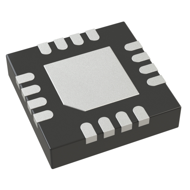
| Package / Case | 20-SOIC (0.295", 7.50mm Width) | 20-VFQFN Exposed Pad (3x3) |
| Product Status | Obsolete | Active |
| Moisture Sensitivity Level (MSL) | 1 (Unlimited) | 1 (Unlimited) |
| RoHS Status | Not specified | ROHS3 Compliant |
Engineering Selection Recommendations
The 74FCT3807SNDGI8 is the manufacturer-recommended substitute for the obsolete 74FCT807BTSOG8. Key selection considerations:
Product Status: The 74FCT3807SNDGI8 maintains active production status, ensuring long-term availability and supply chain stability compared to the obsolete 74FCT807BTSOG8.
Compliance & Certifications: The 74FCT3807SNDGI8 is ROHS3 compliant, meeting current environmental and regulatory requirements. Both parts maintain REACH Unaffected status and EAR99 export classification.
Performance Enhancement: The substitute provides doubled maximum frequency (200 MHz versus 100 MHz) and extended operating temperature range (-40°C to 105°C versus 0°C to 70°C), offering improved performance margins for demanding applications.
Package Transition: The substitute transitions from 20-SOIC to 20-VFQFN Exposed Pad packaging. While both are surface-mount solutions with similar pin counts, PCB layout modifications are required to accommodate the different package footprint and dimensions.
Logic Level Compatibility: The substitute accepts LVTTL input and provides both CMOS and TTL output options, maintaining backward compatibility with TTL-based systems while offering flexibility for mixed-signal designs.
Frequently Asked Questions (FAQ)
Q: Can the 74FCT3807SNDGI8 directly replace the 74FCT807BTSOG8 without PCB modifications?
A: No. While both devices provide 1:10 clock fanout functionality, the package transition from 20-SOIC to 20-VFQFN requires PCB layout changes. The footprints, pin spacing, and mounting requirements differ. A new PCB design or rework is necessary.
Q: What is the impact of the different supply voltage ranges?
A: The 74FCT807BTSOG8 requires 4.75V to 5.25V, while the 74FCT3807SNDGI8 operates on 1.71V to 3.45V. If your system uses 5V logic, the substitute requires a separate 3.3V or lower supply rail. Verify your power distribution architecture supports this requirement.
Q: Does the LVTTL input on the 74FCT3807SNDGI8 work with TTL output signals?
A: Yes. LVTTL (Low Voltage TTL) input is backward-compatible with standard TTL output levels. The substitute will correctly interpret TTL-level input signals from the previous stage.
Q: Why is the operating temperature range wider on the substitute?
A: The 74FCT3807SNDGI8 supports -40°C to 105°C, compared to 0°C to 70°C on the original. This reflects modern manufacturing standards and provides additional margin for industrial and extended-temperature applications. Your design may not require this extended range.
Q: Is the doubled frequency (200 MHz) a requirement for substitution?
A: No. The 200 MHz maximum frequency on the 74FCT3807SNDGI8 exceeds the original 100 MHz specification, providing performance headroom. If your application operates at or below 100 MHz, the substitute remains fully compatible.
Q: What does "Exposed Pad" mean in the 20-VFQFN package?
A: The exposed pad is a thermal and electrical connection point on the bottom of the package. It must be soldered to the PCB for proper thermal management and electrical performance. Ensure your PCB design includes appropriate via patterns and thermal relief structures for this pad.
Q: Are there any signal integrity differences between the packages?
A: The 20-VFQFN package typically offers improved signal integrity characteristics compared to 20-SOIC due to shorter lead lengths and reduced parasitic inductance. This supports the higher 200 MHz frequency capability.
Alternative Parts

SJ6012L2TP
Littelfuse Inc.
6 Alternative Parts

JMK107BBJ476MA-RE
Taiyo Yuden
10 Alternative Parts

GMK107BBJ475MA-T
Taiyo Yuden
5 Alternative Parts
SJ6020N2ARP
Littelfuse Inc.
3 Alternative Parts
SJ6025R2ATP
Littelfuse Inc.
4 Alternative Parts

2474-05L
API Delevan Inc.
1 Alternative Parts

4590R-684K
API Delevan Inc.
1 Alternative Parts

CM6560R-334
API Delevan Inc.
1 Alternative Parts

CM6460-104
API Delevan Inc.
1 Alternative Parts

5526-12
API Delevan Inc.
1 Alternative Parts