


Request Quote
(Ships tomorrow)
74ACTQ273SJX Equivalent & Substitute Parts
Part Overview
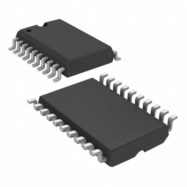
The 74ACTQ273SJX is a D-Type flip-flop logic integrated circuit manufactured by onsemi, featuring 1 element with 8-bit configuration and positive edge triggering. This component is classified as obsolete, making identification of suitable substitute parts essential for ongoing design support and production continuity. The part operates at a maximum clock frequency of 189 MHz with a propagation delay of 8.5ns at 5V with 50pF load, housed in a 20-SOIC surface mount package.
Substiute Parts
Key Parameters
| Parameter | Value |
|---|---|
| Manufacturer Part Number | 74ACTQ273SJX |
| Manufacturer | onsemi |
| Category | Logic |
| Type | D-Type Flip Flop |
| Number of Elements | 1 |
| Number of Bits per Element | 8 |
| Clock Frequency | 189 MHz |
| Max Propagation Delay @ 5V, 50pF | 8.5ns |
| Trigger Type | Positive Edge |
| Output Type | Non-Inverted |
| Voltage Supply Range | 4.5V ~ 5.5V |
| Current Output High/Low | 24mA / 24mA |
| Quiescent Current (Iq) | 40 µA |
| Operating Temperature | -40°C ~ 85°C |
| Package Type | 20-SOIC (0.209", 5.30mm Width) |
| Mounting Type | Surface Mount |
| Product Status | Obsolete |
| Moisture Sensitivity Level | 1 (Unlimited) |
Substitute Part Grouping Explanation
Substitution of the 74ACTQ273SJX is determined by the following critical parameters:
Functional Compatibility:
- D-Type flip-flop architecture with 1 element, 8-bit configuration
- Positive edge trigger mechanism
- Non-inverted output type
- Master reset function
Electrical Compatibility:
- Supply voltage range: 4.5V ~ 5.5V
- Output drive capability: 24mA minimum (both high and low states)
- Trigger type: Positive edge
Physical Compatibility:
- 20-SOIC surface mount package
- Pin configuration alignment with 74ACT series logic devices
The CD74ACT273M96 from Texas Instruments meets these core substitution criteria as an active product within the 74ACT logic family, maintaining functional equivalence while offering extended operating temperature range and improved availability.
Parameter Comparison
| Parameter | 74ACTQ273SJX (onsemi) | CD74ACT273M96 (Texas Instruments) |
|---|---|---|
| Type | D-Type Flip Flop | D-Type Flip Flop |
| Number of Elements | 1 | 1 |
| Number of Bits per Element | 8 | 8 |
| Trigger Type | Positive Edge | Positive Edge |
| Output Type | Non-Inverted | Non-Inverted |
| Function | Master Reset | Master Reset |
| Clock Frequency | 189 MHz | 80 MHz |
| Max Propagation Delay @ 5V, 50pF | 8.5ns | 14.6ns |
| Voltage Supply Range | 4.5V ~ 5.5V | 4.5V ~ 5.5V |
| Current Output High/Low | 24mA / 24mA | 24mA / 24mA |
| Quiescent Current (Iq) | 40 µA | 8 µA |
| Operating Temperature Range | -40°C ~ 85°C | -55°C ~ 125°C |
| Package Type | 20-SOIC (0.209", 5.30mm Width) | 20-SOIC (0.295", 7.50mm Width) |
| Mounting Type | Surface Mount | Surface Mount |
| Product Status | Obsolete | Active |
| Moisture Sensitivity Level | 1 (Unlimited) | 1 (Unlimited) |
| RoHS Status | Not specified | ROHS3 Compliant |
Engineering Selection Recommendations
The CD74ACT273M96 serves as a functional substitute for the obsolete 74ACTQ273SJX based on the following engineering criteria:
Product Status Consideration: The 74ACTQ273SJX is classified as obsolete, creating supply chain risk. The CD74ACT273M96 maintains active product status from Texas Instruments, ensuring long-term availability and manufacturing support.
Compliance and Certification: The CD74ACT273M96 is ROHS3 compliant, meeting current environmental and regulatory requirements. Both parts maintain REACH unaffected status and EAR99 export classification.
Functional Equivalence: Both devices implement identical D-Type flip-flop architecture with 8-bit configuration, positive edge triggering, and non-inverted outputs. Master reset functionality is preserved across both parts.
Electrical Parameters: Supply voltage ranges are identical (4.5V ~ 5.5V). Output drive capability matches at 24mA for both high and low states. The CD74ACT273M96 exhibits lower quiescent current (8 µA versus 40 µA), providing improved power efficiency.
Operating Temperature: The CD74ACT273M96 extends the operating temperature range to -55°C ~ 125°C compared to the original -40°C ~ 85°C specification, offering broader environmental compatibility.
Package Consideration: Both parts use 20-SOIC surface mount packaging. Physical dimensions differ slightly (0.209" versus 0.295" width), but both conform to standard 20-SOIC footprint specifications suitable for PCB integration.
Frequently Asked Questions (FAQ)
Q: Can the CD74ACT273M96 directly replace the 74ACTQ273SJX in existing designs?
A: Yes, the CD74ACT273M96 provides functional equivalence for the 74ACTQ273SJX. Both devices implement identical D-Type flip-flop logic with 8-bit configuration, positive edge triggering, and non-inverted outputs. Electrical parameters including supply voltage (4.5V ~ 5.5V) and output drive capability (24mA) are matched. PCB footprints are compatible as both use 20-SOIC surface mount packages.
Q: What are the key differences between these two parts?
A: The primary differences are: (1) Product status—the 74ACTQ273SJX is obsolete while the CD74ACT273M96 is active; (2) Clock frequency—189 MHz versus 80 MHz; (3) Propagation delay—8.5ns versus 14.6ns at 5V with 50pF load; (4) Quiescent current—40 µA versus 8 µA; (5) Operating temperature range—-40°C ~ 85°C versus -55°C ~ 125°C; (6) RoHS compliance—the CD74ACT273M96 is ROHS3 compliant.
Q: Are there package dimension concerns when substituting these parts?
A: Both parts use 20-SOIC surface mount packaging. The 74ACTQ273SJX measures 0.209" width (5.30mm) while the CD74ACT273M96 measures 0.295" width (7.50mm). Both conform to standard 20-SOIC footprint specifications. PCB designs using standard 20-SOIC land patterns will accommodate both parts without modification.
Q: Does the lower clock frequency of the CD74ACT273M96 affect system performance?
A: The CD74ACT273M96 operates at 80 MHz compared to the 74ACTQ273SJX at 189 MHz. This difference is application-dependent. If your system clock frequency is below 80 MHz, the substitute part operates within specification. If your design requires operation above 80 MHz, the propagation delay characteristics must be evaluated against system timing requirements.
Q: What is the significance of the lower quiescent current in the CD74ACT273M96?
A: The CD74ACT273M96 draws 8 µA quiescent current versus 40 µA for the 74ACTQ273SJX. This 5-fold reduction in standby current consumption provides power efficiency benefits, particularly in battery-powered or low-power applications where quiescent current contributes significantly to overall power budget.
Q: Are both parts suitable for industrial temperature applications?
A: The 74ACTQ273SJX operates from -40°C ~ 85°C. The CD74ACT273M96 extends this range to -55°C ~ 125°C, providing broader environmental compatibility. For applications requiring operation below -40°C or above 85°C, the CD74ACT273M96 offers extended temperature coverage.
Alternative Parts

SJ6012L2TP
Littelfuse Inc.
6 Alternative Parts

JMK107BBJ476MA-RE
Taiyo Yuden
10 Alternative Parts

GMK107BBJ475MA-T
Taiyo Yuden
5 Alternative Parts
SJ6020N2ARP
Littelfuse Inc.
3 Alternative Parts
SJ6025R2ATP
Littelfuse Inc.
4 Alternative Parts

2474-05L
API Delevan Inc.
1 Alternative Parts

4590R-684K
API Delevan Inc.
1 Alternative Parts

CM6560R-334
API Delevan Inc.
1 Alternative Parts

CM6460-104
API Delevan Inc.
1 Alternative Parts

5526-12
API Delevan Inc.
1 Alternative Parts