


Request Quote
(Ships tomorrow)
Equivalent & Substitute Parts for 7202LA30DB
Part Overview
The 7202LA30DB is an asynchronous FIFO (First-In-First-Out) memory IC manufactured by Renesas Electronics Corporation. This device provides 9K (1K x 9) storage capacity with uni-directional bus architecture, designed for applications requiring temporary data buffering with asynchronous read/write operations. The part is classified as obsolete, making identification of suitable substitute components essential for ongoing system support and new design implementations.
Substiute Parts
Key Parameters
| Parameter | Value |
|---|---|
| Manufacturer | Renesas Electronics Corporation |
| Memory Size | 9K (1K x 9) |
| Function | Asynchronous |
| Data Rate | 25MHz |
| Access Time | 30ns |
| Voltage Supply | 4.5V ~ 5.5V |
| Current Supply (Max) | 100mA |
| Bus Directional | Uni-Directional |
| Operating Temperature | -55°C ~ 125°C |
| Package Type | 28-CDIP (0.600", 15.24mm) |
| Mounting Type | Through Hole |
| Product Status | Obsolete |
| RoHS Status | RoHS non-compliant |
Substitute Part Grouping Explanation
Substitution eligibility for the 7202LA30DB is determined by the following critical parameters:
Core Functional Requirements:
- Memory capacity: 9K (1K x 9)
- FIFO function: Asynchronous operation
- Bus architecture: Uni-Directional
- Voltage supply range: 4.5V ~ 5.5V
Performance Characteristics:
- Data rate capability: Minimum 25MHz
- Access time: Maximum 30ns or faster
- Current supply: Within acceptable operating limits
Physical and Environmental Constraints:
- Operating temperature range compatibility
- Mounting type and package form factor
- Compliance certifications and regulatory status
The 7202LA12JG qualifies as a substitute because it maintains identical memory capacity, asynchronous FIFO function, uni-directional bus architecture, and compatible voltage supply specifications. The substitute part exceeds the performance requirements of the original part with faster access time (12ns vs. 30ns) and higher data rate capability (50MHz vs. 25MHz), ensuring functional compatibility in applications designed for the 7202LA30DB.
Parameter Comparison
| Parameter | 7202LA30DB (Main Part) | 7202LA12JG (Substitute) |
|---|---|---|
| Manufacturer | Renesas Electronics Corporation | Renesas Electronics Corporation |
| Memory Size | 9K (1K x 9) | 9K (1K x 9) |
| Function | Asynchronous | Asynchronous |
| Data Rate | 25MHz | 50MHz |
| Access Time | 30ns | 12ns |
| Voltage Supply | 4.5V ~ 5.5V | 4.5V ~ 5.5V |
| Current Supply (Max) | 100mA | 80mA |
| Bus Directional | Uni-Directional | Uni-Directional |
| Operating Temperature | -55°C ~ 125°C | 0°C ~ 70°C |
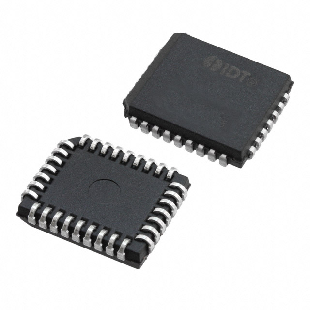
| Package Type | 28-CDIP (0.600", 15.24mm) | 32-PLCC (14x11.46) |
| Mounting Type | Through Hole | Surface Mount |
| Product Status | Obsolete | Active |
| RoHS Status | RoHS non-compliant | ROHS3 Compliant |
Engineering Selection Recommendations
The 7202LA12JG is the manufacturer-recommended substitute for the obsolete 7202LA30DB. Selection of this substitute is supported by the following engineering considerations:
Functional Compatibility: Both parts share identical memory architecture (9K, 1K x 9), asynchronous FIFO operation, and uni-directional bus configuration. The substitute maintains full functional equivalence for applications originally designed with the 7202LA30DB.
Performance Enhancement: The 7202LA12JG provides superior performance specifications with 12ns access time and 50MHz data rate capability, exceeding the original part's 30ns access time and 25MHz rating. This performance margin ensures the substitute operates within design specifications for legacy applications.
Supply Voltage Compatibility: Both parts operate within the identical 4.5V to 5.5V supply voltage range, eliminating power supply redesign requirements.
Product Status and Compliance: The 7202LA12JG holds active product status with ROHS3 compliance certification, providing long-term availability and regulatory alignment. The original 7202LA30DB is obsolete and RoHS non-compliant, making transition to the substitute necessary for new designs and ongoing system support.
Design Considerations: The substitute employs surface mount packaging (32-PLCC) versus the original through-hole package (28-CDIP). PCB layout and assembly process modifications are required. The substitute's operating temperature range (0°C to 70°C) is narrower than the original (-55°C to 125°C), requiring verification for applications requiring extended temperature operation.
Frequently Asked Questions (FAQ)
Q: Can the 7202LA12JG directly replace the 7202LA30DB without circuit modifications?
A: Functional replacement is possible because both parts maintain identical memory capacity, asynchronous FIFO operation, and uni-directional bus architecture with compatible voltage supply specifications. However, physical integration requires PCB redesign due to different package types (28-CDIP through-hole versus 32-PLCC surface mount). Pin-to-pin compatibility must be verified against specific application schematics.
Q: What are the key differences between these two parts?
A: The primary differences are access time (30ns vs. 12ns), data rate (25MHz vs. 50MHz), package type (28-CDIP vs. 32-PLCC), mounting method (through-hole vs. surface mount), operating temperature range (-55°C to 125°C vs. 0°C to 70°C), and product status (obsolete vs. active). The substitute provides faster performance and modern compliance certifications.
Q: Is the 7202LA12JG suitable for applications requiring extended temperature operation below 0°C or above 70°C?
A: The 7202LA12JG operating temperature range is 0°C to 70°C. Applications requiring operation outside this range must evaluate alternative components or confirm that the narrower temperature specification meets actual system requirements.
Q: What packaging and mounting considerations apply when substituting the 7202LA12JG?
A: The original 7202LA30DB uses 28-CDIP through-hole packaging, while the 7202LA12JG uses 32-PLCC surface mount packaging. PCB layout modifications, assembly process changes, and socket/connector redesign are necessary. The 32-PLCC package dimensions are 14mm x 11.46mm.
Q: Are there compliance or regulatory differences between these parts?
A: The 7202LA30DB is RoHS non-compliant, while the 7202LA12JG is ROHS3 compliant. Both parts share identical REACH and ECCN classifications. New designs should prioritize the compliant 7202LA12JG to meet current regulatory requirements.
Q: What is the current supply difference between these parts?
A: The 7202LA30DB maximum supply current is 100mA, while the 7202LA12JG maximum supply current is 80mA. The substitute requires lower current, potentially reducing power dissipation and thermal management requirements.
Alternative Parts

SJ6012L2TP
Littelfuse Inc.
6 Alternative Parts

JMK107BBJ476MA-RE
Taiyo Yuden
10 Alternative Parts

GMK107BBJ475MA-T
Taiyo Yuden
5 Alternative Parts
SJ6020N2ARP
Littelfuse Inc.
3 Alternative Parts
SJ6025R2ATP
Littelfuse Inc.
4 Alternative Parts

2474-05L
API Delevan Inc.
1 Alternative Parts

4590R-684K
API Delevan Inc.
1 Alternative Parts

CM6560R-334
API Delevan Inc.
1 Alternative Parts

CM6460-104
API Delevan Inc.
1 Alternative Parts

5526-12
API Delevan Inc.
1 Alternative Parts