


Request Quote
(Ships tomorrow)
Renesas 552AR-01LFT Clock Generator Equivalent & Substitute Parts
Part Overview
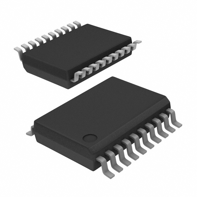
The 552AR-01LFT is a Clock Generator and Fanout Distribution IC manufactured by Renesas Electronics Corporation, designed for 200MHz clock distribution applications. This device features a 1:8 input-to-output ratio with CMOS output configuration and operates across a 3V to 5.5V supply voltage range in a 20-SSOP surface mount package.
The 552AR-01LFT is classified as an obsolete product. Identifying equivalent and substitute parts is necessary to maintain system continuity, ensure design flexibility, and support long-term production requirements when original inventory becomes unavailable.
Substiute Parts
Key Parameters
| Parameter | Specification |
|---|---|
| Manufacturer | Renesas Electronics Corporation |
| Category | Clock/Timing |
| Type | Clock Generator, Fanout Distribution |
| Frequency - Max | 200 MHz |
| Ratio - Input:Output | 1:8 |
| Output Type | CMOS |
| Voltage - Supply | 3V ~ 5.5V |
| Operating Temperature | 0°C ~ 70°C |
| Mounting Type | Surface Mount |
| Package / Case | 20-SSOP (0.154", 3.90mm Width) |
| Product Status | Obsolete |
Substitute Part Grouping Explanation
Substitution eligibility for the 552AR-01LFT is determined by the following critical parameters:
- Frequency Capability: Maximum operating frequency must be 200 MHz or greater
- Input-to-Output Ratio: Must maintain 1:8 distribution configuration
- Output Logic Family: CMOS or compatible logic standard (LVCMOS acceptable)
- Supply Voltage Compatibility: Operating voltage range must overlap with or encompass the original 3V to 5.5V specification
- Differential Characteristics: Both input and output must be non-differential
- Mounting Technology: Surface mount configuration required
- Manufacturer: Renesas Electronics Corporation maintains design continuity
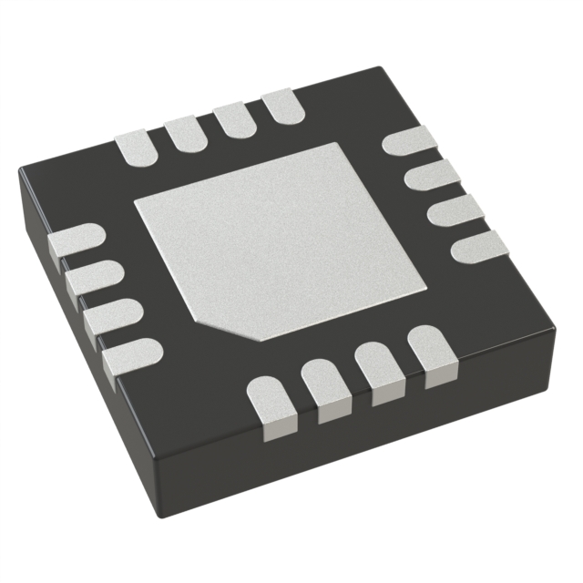
The 5P83908NDGK8 qualifies as a direct substitute based on these parameters. Both devices share identical frequency specifications, input-to-output ratios, and non-differential signal characteristics. The substitute operates at a lower supply voltage range (1.71V to 3.465V) with an extended operating temperature range (-40°C to 105°C), providing enhanced performance margins for modern applications.
Parameter Comparison
| Parameter | 552AR-01LFT (Original) | 5P83908NDGK8 (Substitute) |
|---|---|---|
| Manufacturer | Renesas Electronics Corporation | Renesas Electronics Corporation |
| Category | Clock/Timing | Clock/Timing |
| Type | Clock Generator, Fanout Distribution | Fanout Buffer (Distribution) |
| Frequency - Max | 200 MHz | 200 MHz |
| Ratio - Input:Output | 1:8 | 1:8 |
| Output Logic | CMOS | LVCMOS |
| Differential - Input:Output | No/No | No/No |
| Voltage - Supply | 3V ~ 5.5V | 1.71V ~ 3.465V |
| Operating Temperature | 0°C ~ 70°C | -40°C ~ 105°C |
| Mounting Type | Surface Mount | Surface Mount |
| Package / Case | 20-SSOP (0.154", 3.90mm Width) | 20-VFQFN Exposed Pad (3x3) |
| Product Status | Obsolete | Active |
| RoHS Status | Not specified | ROHS3 Compliant |
| Moisture Sensitivity Level | 1 (Unlimited) | 1 (Unlimited) |
Engineering Selection Recommendations
The 5P83908NDGK8 is the qualified substitute for the 552AR-01LFT based on functional equivalence and compliance status.
Product Status Consideration: The original 552AR-01LFT is obsolete, while the 5P83908NDGK8 maintains active production status. This ensures long-term availability and supply chain stability for new designs and production continuity.
Compliance and Certification: The 5P83908NDGK8 carries ROHS3 compliance certification, meeting current environmental and regulatory requirements. Both devices share identical REACH status (REACH Unaffected) and ECCN classification (EAR99), ensuring consistent regulatory treatment.
Package Transition: The substitute employs a 20-VFQFN Exposed Pad package (3x3mm) in place of the original 20-SSOP package. This represents a standard industry transition to more compact, thermally efficient packaging. PCB layout modifications are required to accommodate the different footprint geometry.
Voltage and Temperature Performance: The substitute operates within a lower supply voltage range (1.71V to 3.465V) with an extended operating temperature specification (-40°C to 105°C). Applications operating within the original 3V to 5.5V range will function within the substitute's specified voltage window. The expanded temperature range provides additional operational margin for demanding environments.
Frequently Asked Questions (FAQ)
Q: Can the 5P83908NDGK8 directly replace the 552AR-01LFT without circuit modifications?
A: Functional substitution is valid based on matching frequency, input-to-output ratio, and logic characteristics. However, package geometry differs (20-SSOP versus 20-VFQFN), requiring PCB layout redesign. Pin-to-pin functional compatibility must be verified against detailed pinout documentation for your specific application.
Q: What is the impact of the different package types on board design?
A: The original 20-SSOP package (0.154" width, 3.90mm) differs from the substitute 20-VFQFN package (3x3mm). The VFQFN package is more compact and includes an exposed thermal pad for improved heat dissipation. PCB footprint, trace routing, and thermal management strategies require redesign to accommodate the new package geometry.
Q: Is the lower supply voltage range of the substitute a limitation?
A: The substitute operates at 1.71V to 3.465V, which overlaps the original 3V to 5.5V range at the lower end. Applications designed for 3V to 3.465V operation will function identically. Applications requiring operation above 3.465V cannot use this substitute without circuit redesign to reduce supply voltage.
Q: What are the advantages of selecting the active substitute over the obsolete original?
A: The 5P83908NDGK8 is in active production, ensuring consistent availability and supply chain reliability. It carries ROHS3 compliance certification and provides an extended operating temperature range (-40°C to 105°C versus 0°C to 70°C), offering greater design flexibility for industrial and extended-temperature applications.
Q: Are there any differences in input signal requirements between the two devices?
A: Both devices accept crystal and clock inputs with non-differential signal characteristics. Detailed input impedance, rise time, and duty cycle specifications should be cross-referenced in the respective device datasheets to ensure signal integrity in your specific application circuit.
Alternative Parts

SJ6012L2TP
Littelfuse Inc.
6 Alternative Parts

JMK107BBJ476MA-RE
Taiyo Yuden
10 Alternative Parts

GMK107BBJ475MA-T
Taiyo Yuden
5 Alternative Parts
SJ6020N2ARP
Littelfuse Inc.
3 Alternative Parts
SJ6025R2ATP
Littelfuse Inc.
4 Alternative Parts

2474-05L
API Delevan Inc.
1 Alternative Parts

4590R-684K
API Delevan Inc.
1 Alternative Parts

CM6560R-334
API Delevan Inc.
1 Alternative Parts

CM6460-104
API Delevan Inc.
1 Alternative Parts

5526-12
API Delevan Inc.
1 Alternative Parts