


Request Quote
(Ships tomorrow)
49FCT805APYGI8 Equivalent & Substitute Parts
Part Overview
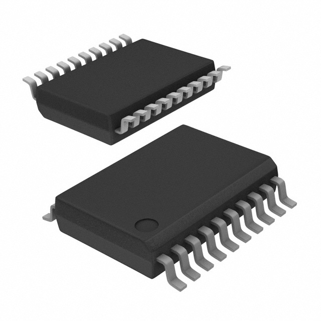
The 49FCT805APYGI8 is a Clock Fanout Buffer (Distribution) IC manufactured by Renesas Electronics Corporation, featuring a 1:5 input-to-output ratio in a 20-SSOP package. This part is classified as obsolete, making identification of functionally equivalent alternatives essential for ongoing system support and new design implementations. The device provides clock distribution capabilities with CMOS and LVTTL input/output compatibility, operating across the industrial temperature range of -40°C to 85°C.
Substiute Parts
Key Parameters
| Parameter | Value |
|---|---|
| Manufacturer Part Number | 49FCT805APYGI8 |
| Manufacturer | Renesas Electronics Corporation |
| Category | Clock/Timing |
| Type | Fanout Buffer (Distribution) |
| Ratio - Input:Output | 1:5 |
| Number of Circuits | 2 |
| Input Type | CMOS, LVTTL |
| Output Type | CMOS, LVTTL |
| Voltage - Supply | 4.75V ~ 5.25V |
| Operating Temperature | -40°C ~ 85°C |
| Package / Case | 20-SSOP (0.209", 5.30mm Width) |
| Mounting Type | Surface Mount |
| Product Status | Obsolete |
| RoHS Status | ROHS3 Compliant |
Substitute Part Grouping Explanation
Substitution eligibility for the 49FCT805APYGI8 is determined by the following critical parameters:
Primary Substitution Criteria:
- Input-to-output ratio of 1:5
- Fanout buffer (distribution) functionality
- CMOS and LVTTL input/output compatibility
- Surface mount packaging
- Operating temperature range of -40°C to 85°C
- RoHS3 compliance
Secondary Compatibility Factors:
- Package form factor (20-SSOP preferred for direct PCB compatibility)
- Supply voltage range (5V nominal operation or compatible logic levels)
- Number of circuits (2 circuits in main part)
The substitute parts listed below meet the primary substitution criteria. Variations in package type, supply voltage, and maximum frequency do not preclude functional substitution when system requirements permit.
Parameter Comparison
| Parameter | 49FCT805APYGI8 | 8L30210NLGI8 | PI49FCT3805CHE | PI49FCT3805DHEX |
|---|---|---|---|---|
| Manufacturer | Renesas Electronics | Renesas Electronics | Diodes Incorporated | Diodes Incorporated |
| Type | Fanout Buffer | Clock Buffer | Fanout Buffer | Fanout Buffer |
| Ratio - Input:Output | 1:5 | 3:10 | 1:5 | 1:5 |
| Number of Circuits | 2 | 1 | 2 | 2 |
| Input Type | CMOS, LVTTL | HCSL, LVCMOS, LVDS, LVPECL, LVTTL, Crystal | CMOS, TTL | CMOS, TTL |
| Output Type | CMOS, LVTTL | LVCMOS, LVTTL | CMOS | CMOS |
| Frequency - Max | Not specified | 200 MHz | 100 MHz | 133 MHz |
| Voltage - Supply | 4.75V ~ 5.25V | 1.4V ~ 3.465V | 3V ~ 3.6V | 3V ~ 3.6V |
| Operating Temperature | -40°C ~ 85°C | -40°C ~ 85°C | -40°C ~ 85°C | -40°C ~ 85°C |
| Package / Case | 20-SSOP | 32-VFQFN Exposed Pad | 20-SSOP | 20-SSOP |
| Product Status | Obsolete | Active | Active | Active |
| RoHS Status | ROHS3 Compliant | ROHS3 Compliant | ROHS3 Compliant | ROHS3 Compliant |
Engineering Selection Recommendations
PI49FCT3805CHE and PI49FCT3805DHEX (Diodes Incorporated)
These parts represent the closest functional equivalents to the 49FCT805APYGI8. Both maintain the 1:5 input-to-output ratio, 2-circuit configuration, and 20-SSOP package form factor. The PI49FCT3805CHE operates at 100 MHz maximum frequency, while the PI49FCT3805DHEX extends this to 133 MHz. Both are active products with ROHS3 compliance and identical operating temperature ranges. Supply voltage operates at 3V to 3.6V, requiring voltage level consideration in 5V systems. These parts are suitable for direct PCB footprint replacement when system voltage requirements are compatible.
8L30210NLGI8 (Renesas Electronics Corporation)
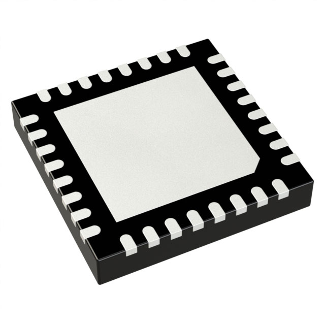
This part shares manufacturer lineage with the obsolete 49FCT805APYGI8 and maintains active product status with ROHS3 compliance. However, it differs in several parameters: the 3:10 input-to-output ratio, single-circuit configuration, and 32-VFQFN package form factor require PCB redesign. The extended input compatibility (HCSL, LVDS, LVPECL, Crystal) and higher maximum frequency (200 MHz) provide enhanced capabilities. Supply voltage operates at 1.4V to 3.465V. This part is suitable for new designs where package redesign is feasible.
Frequently Asked Questions (FAQ)
Q: Can PI49FCT3805CHE or PI49FCT3805DHEX be used as direct replacements for 49FCT805APYGI8?
A: Both Diodes Incorporated parts maintain the same 20-SSOP package and 1:5 ratio with 2 circuits, enabling direct PCB footprint compatibility. However, the supply voltage range differs (3V to 3.6V versus 4.75V to 5.25V). System voltage compatibility must be verified before implementation.
Q: What is the primary difference between PI49FCT3805CHE and PI49FCT3805DHEX?
A: Both parts are functionally identical except for maximum frequency specification. The PI49FCT3805CHE operates to 100 MHz, while the PI49FCT3805DHEX extends to 133 MHz. Selection depends on system clock frequency requirements.
Q: Why does 8L30210NLGI8 have a different input-to-output ratio?
A: The 8L30210NLGI8 is a different product line within Renesas' clock buffer portfolio, designed for applications requiring 3:10 distribution. The 1:5 ratio of the 49FCT805APYGI8 is maintained only in the Diodes Incorporated PI49FCT3805 series.
Q: Are all substitute parts RoHS3 compliant?
A: Yes. The 49FCT805APYGI8 and all listed substitute parts carry ROHS3 compliance certification, meeting environmental regulatory requirements.
Q: What packaging considerations apply to the 8L30210NLGI8?
A: The 8L30210NLGI8 uses a 32-VFQFN Exposed Pad package, which differs from the 20-SSOP of the original part. PCB layout redesign is required for implementation.
Alternative Parts

SJ6012L2TP
Littelfuse Inc.
6 Alternative Parts

JMK107BBJ476MA-RE
Taiyo Yuden
10 Alternative Parts

GMK107BBJ475MA-T
Taiyo Yuden
5 Alternative Parts
SJ6020N2ARP
Littelfuse Inc.
3 Alternative Parts
SJ6025R2ATP
Littelfuse Inc.
4 Alternative Parts

2474-05L
API Delevan Inc.
1 Alternative Parts

4590R-684K
API Delevan Inc.
1 Alternative Parts

CM6560R-334
API Delevan Inc.
1 Alternative Parts

CM6460-104
API Delevan Inc.
1 Alternative Parts

5526-12
API Delevan Inc.
1 Alternative Parts