


Request Quote
(Ships tomorrow)
3STL2540 Equivalent & Substitute Parts
Part Overview
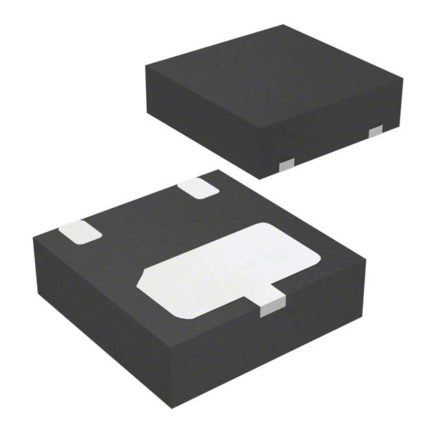
The 3STL2540 is a Bipolar (BJT) Transistor manufactured by STMicroelectronics, classified as a PNP-type device rated for 40 V collector-emitter breakdown voltage and 5 A maximum collector current. The device is packaged in a Surface Mount PowerFlat™ (2x2) configuration and delivers 1.2 W maximum power dissipation with a transition frequency of 130 MHz.
The 3STL2540 carries an Obsolete product status. Identification of equivalent and substitute parts is necessary to maintain design continuity, ensure supply chain availability, and support ongoing production requirements for applications utilizing this component.
Substiute Parts
Key Parameters
| Parameter | Value |
|---|---|
| Transistor Type | PNP |
| Current - Collector (Ic) (Max) | 5 A |
| Voltage - Collector Emitter Breakdown (Max) | 40 V |
| Power - Max | 1.2 W |
| Frequency - Transition | 130 MHz |
| Mounting Type | Surface Mount |
| Package / Case | 3-PowerUDFN (2x2) |
| RoHS Status | ROHS3 Compliant |
| Moisture Sensitivity Level (MSL) | 1 (Unlimited) |
Substitute Part Grouping Explanation
Substitution of the 3STL2540 is determined by strict equivalence across the following electrical and mechanical parameters:
Electrical Equivalence Criteria:
- Transistor Type: PNP
- Maximum Collector Current (Ic): 5 A
- Maximum Collector-Emitter Breakdown Voltage: 40 V
- Mounting Type: Surface Mount
Mechanical Compatibility Criteria:
- Package form factor: 2x2 mm footprint configuration
- Surface Mount technology compatibility
Compliance Requirements:
- RoHS3 Compliance
- Moisture Sensitivity Level 1 (Unlimited)
The NSS40500UW3T2G from onsemi meets all electrical equivalence criteria and compliance requirements. While the package designation differs (3-WDFN versus 3-PowerUDFN), both employ identical 2x2 mm surface mount footprints with exposed pad configurations, ensuring mechanical and thermal compatibility in PCB layouts designed for the 3STL2540.
Parameter Comparison
| Parameter | 3STL2540 (STMicroelectronics) | NSS40500UW3T2G (onsemi) |
|---|---|---|
| Transistor Type | PNP | PNP |
| Current - Collector (Ic) (Max) | 5 A | 5 A |
| Voltage - Collector Emitter Breakdown (Max) | 40 V | 40 V |
| Vce Saturation (Max) @ Ib, Ic | 200 mV @ 10 mA, 1 A | 260 mV @ 400 mA, 4 A |
| Current - Collector Cutoff (Max) | 100 nA (ICBO) | 100 nA (ICBO) |
| DC Current Gain (hFE) (Min) @ Ic, Vce | 210 @ 2 A, 2 V | 180 @ 2 A, 2 V |
| Power - Max | 1.2 W | 875 mW |
| Frequency - Transition | 130 MHz | 100 MHz |
| Operating Temperature (TJ) | 150°C | -55°C ~ 150°C |
| Mounting Type | Surface Mount | Surface Mount |
| Package / Case | 3-PowerUDFN (2x2) | 3-WDFN Exposed Pad (2x2) |
| RoHS Status | ROHS3 Compliant | ROHS3 Compliant |
| Moisture Sensitivity Level (MSL) | 1 (Unlimited) | 1 (Unlimited) |
| Product Status | Obsolete | Active |
Engineering Selection Recommendations
The NSS40500UW3T2G qualifies as a direct substitute for the 3STL2540 based on electrical parameter equivalence and compliance alignment. Both devices are ROHS3 compliant and carry MSL 1 (Unlimited) moisture sensitivity ratings, ensuring compatibility with standard manufacturing and storage protocols.
The 3STL2540 is classified as Obsolete, whereas the NSS40500UW3T2G maintains Active product status. Selection of the NSS40500UW3T2G provides access to current manufacturing inventory and ongoing supplier support, eliminating supply chain risk associated with obsolete component sourcing.
Differences in maximum power dissipation (1.2 W versus 875 mW) and transition frequency (130 MHz versus 100 MHz) are secondary considerations. Applications operating within the NSS40500UW3T2G power and frequency specifications will function without modification. Applications requiring the full 1.2 W power envelope or 130 MHz transition frequency performance must evaluate thermal and frequency margins within the design context.
Frequently Asked Questions (FAQ)
Q: Can the NSS40500UW3T2G directly replace the 3STL2540 in existing PCB designs?
A: Yes. Both devices employ identical 2x2 mm surface mount footprints with exposed pad configurations. PCB layouts designed for the 3STL2540 accommodate the NSS40500UW3T2G without modification. Electrical parameters (5 A collector current, 40 V breakdown voltage, PNP type) are equivalent.
Q: What are the key differences between these two parts?
A: The NSS40500UW3T2G exhibits lower maximum power dissipation (875 mW versus 1.2 W) and lower transition frequency (100 MHz versus 130 MHz). The NSS40500UW3T2G maintains Active product status, whereas the 3STL2540 is Obsolete. DC current gain (hFE) is slightly lower for the NSS40500UW3T2G (180 versus 210 at 2 A, 2 V).
Q: Are there compliance or certification differences?
A: No. Both devices are ROHS3 compliant and carry identical Moisture Sensitivity Level 1 (Unlimited) ratings. REACH status is Unaffected for both parts.
Q: What is the operating temperature range for each device?
A: The 3STL2540 specifies a maximum junction temperature of 150°C. The NSS40500UW3T2G specifies an operating temperature range of -55°C to 150°C, providing extended low-temperature capability.
Q: How do the saturation voltage characteristics compare?
A: The 3STL2540 exhibits 200 mV saturation voltage at 10 mA base current and 1 A collector current. The NSS40500UW3T2G exhibits 260 mV saturation voltage at 400 mA base current and 4 A collector current. These measurements are taken at different operating points and reflect device-specific characterization conditions.
Q: Is the package designation change from PowerFlat™ to 3-WDFN significant?
A: No. Both package designations refer to identical 2x2 mm surface mount configurations with exposed pad thermal management. The functional and mechanical compatibility is maintained.
Alternative Parts

SJ6012L2TP
Littelfuse Inc.
6 Alternative Parts

JMK107BBJ476MA-RE
Taiyo Yuden
10 Alternative Parts

GMK107BBJ475MA-T
Taiyo Yuden
5 Alternative Parts
SJ6020N2ARP
Littelfuse Inc.
3 Alternative Parts
SJ6025R2ATP
Littelfuse Inc.
4 Alternative Parts

2474-05L
API Delevan Inc.
1 Alternative Parts

4590R-684K
API Delevan Inc.
1 Alternative Parts

CM6560R-334
API Delevan Inc.
1 Alternative Parts

CM6460-104
API Delevan Inc.
1 Alternative Parts

5526-12
API Delevan Inc.
1 Alternative Parts