


Request Quote
(Ships tomorrow)
Equivalent & Substitute Parts for Vishay Siliconix 3N164
Part Overview
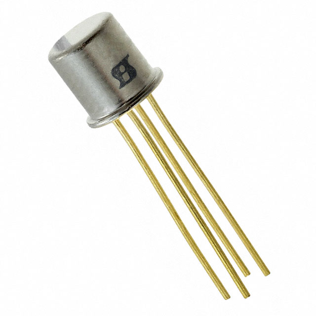
The Vishay Siliconix 3N164 is a P-Channel MOSFET rated for 30 V drain-to-source voltage with 50 mA continuous drain current, packaged in a through-hole TO-72 metal can configuration. This device is classified as obsolete, necessitating identification of functionally equivalent alternatives for ongoing design support and component procurement. The 3N164 operates across an extended temperature range of -55°C to 150°C and dissipates up to 375 mW, making it suitable for low-power switching and analog applications requiring P-Channel enhancement-mode operation.
Substiute Parts
Key Parameters
| Parameter | Value | Unit |
|---|---|---|
| FET Type | P-Channel | — |
| Technology | MOSFET (Metal Oxide) | — |
| Drain to Source Voltage (Vdss) | 30 | V |
| Continuous Drain Current (Id) @ 25°C | 50 | mA |
| Power Dissipation (Max) | 375 | mW |
| Rds On (Max) @ Id, Vgs | 300 | Ohm @ 100µA, 20V |
| Operating Temperature Range | -55 to 150 | °C (TJ) |
| Mounting Type | Through Hole | — |
| Package / Case | TO-206AF, TO-72-4 Metal Can | — |
Substitute Part Grouping Explanation
Substitution of the 3N164 is determined by strict adherence to the following electrical and mechanical parameters:
Primary Substitution Criteria:
- FET Type: P-Channel enhancement-mode operation
- Technology: MOSFET (Metal Oxide Semiconductor)
- Drain-to-Source Voltage (Vdss): Must equal or exceed 30 V
- Continuous Drain Current (Id): Must equal or exceed 50 mA at 25°C
- Power Dissipation: Must equal or exceed 375 mW
- Operating Temperature Range: Must encompass -55°C to 150°C
- Mounting Type: Through Hole configuration
Secondary Compatibility Factors:
- Gate-Source Voltage (Vgs) ratings must be compatible with circuit drive requirements
- On-state resistance (Rds On) characteristics must support application current handling
- Package footprint must accommodate PCB layout constraints
The Diodes Incorporated BS250P satisfies all primary substitution criteria with enhanced electrical performance characteristics, including higher voltage rating (45 V vs. 30 V), increased current capacity (230 mA vs. 50 mA), and superior power dissipation capability (700 mW vs. 375 mW).
Parameter Comparison
| Parameter | 3N164 (Vishay Siliconix) | BS250P (Diodes Incorporated) | Unit |
|---|---|---|---|
| FET Type | P-Channel | P-Channel | — |
| Technology | MOSFET (Metal Oxide) | MOSFET (Metal Oxide) | — |
| Drain to Source Voltage (Vdss) | 30 | 45 | V |
| Continuous Drain Current (Id) @ 25°C | 50 | 230 | mA |
| Power Dissipation (Max) | 375 | 700 | mW |
| Rds On (Max) @ Id, Vgs | 300 @ 100µA, 20V | 14 @ 200mA, 10V | Ohm |
| Vgs(th) (Max) @ Id | 5 @ 10µA | 3.5 @ 1mA | V |
| Vgs (Max) | ±30 | ±20 | V |
| Input Capacitance (Ciss) (Max) @ Vds | 3.5 @ 15V | 60 @ 10V | pF |
| Operating Temperature Range | -55 to 150 | -55 to 150 | °C (TJ) |
| Mounting Type | Through Hole | Through Hole | — |
| Package / Case | TO-206AF, TO-72-4 Metal Can | TO-226-3, TO-92-3 (TO-226AA) | — |
| Product Status | Obsolete | Active | — |
| RoHS Status | RoHS non-compliant | ROHS3 Compliant | — |
Engineering Selection Recommendations
The BS250P from Diodes Incorporated is a direct functional substitute for the obsolete 3N164. The substitute part meets or exceeds all primary electrical parameters required for circuit operation while offering significant advantages in product lifecycle status and regulatory compliance.
Product Status Consideration: The 3N164 is classified as obsolete, whereas the BS250P maintains active product status with established supply chain availability. This distinction is critical for long-term design support and component procurement continuity.
Regulatory Compliance: The BS250P is ROHS3 compliant, whereas the 3N164 is RoHS non-compliant. Both devices are REACH Unaffected and classified under ECCN EAR99 and HTSUS 8541.21.0095.
Electrical Performance: The BS250P provides enhanced electrical performance across all measured parameters. The higher Vdss rating (45 V vs. 30 V) and increased current capacity (230 mA vs. 50 mA) establish a performance margin suitable for applications originally designed around the 3N164 specifications. The lower on-state resistance (14 Ohm vs. 300 Ohm) reduces power dissipation in switching applications.
Package Consideration: The 3N164 uses a TO-72 metal can package, while the BS250P uses a TO-92 package. Both are through-hole configurations; however, PCB layout modifications may be required to accommodate the different footprint geometries.
Frequently Asked Questions (FAQ)
Q: Can the BS250P directly replace the 3N164 without circuit modifications?
A: The BS250P satisfies all primary electrical substitution criteria and operates within the same temperature range. However, the different package footprint (TO-92 vs. TO-72) requires PCB layout adjustment. Circuit operation is compatible without electrical modifications when the package change is accommodated.
Q: What is the significance of the higher Vdss rating on the BS250P?
A: The BS250P's 45 V Vdss rating exceeds the 3N164's 30 V specification, providing additional voltage margin. This characteristic does not compromise compatibility; circuits designed for 30 V operation function correctly with a device rated for 45 V.
Q: How does the lower Rds On of the BS250P affect circuit performance?
A: The BS250P exhibits significantly lower on-state resistance (14 Ohm vs. 300 Ohm), resulting in reduced power dissipation during conduction. This improvement enhances thermal performance and efficiency in switching applications without introducing compatibility issues.
Q: Are there package-related considerations for PCB redesign?
A: Yes. The 3N164 uses a TO-72 metal can package with a different pin configuration and footprint than the BS250P's TO-92 package. PCB layout modifications are necessary to accommodate the substitute part's physical dimensions and pin spacing.
Q: What is the impact of the different Vgs (Max) ratings?
A: The 3N164 permits ±30 V gate-source voltage, while the BS250P permits ±20 V. For applications operating within ±20 V gate drive, this difference is not limiting. Applications requiring gate voltages exceeding ±20 V require circuit evaluation to ensure compatibility.
Q: Does the higher input capacitance of the BS250P affect switching speed?
A: The BS250P exhibits higher input capacitance (60 pF vs. 3.5 pF), which may increase gate charge requirements and switching transition times. Applications with stringent switching speed requirements should evaluate the impact of this parameter on circuit performance.
Q: Is the BS250P suitable for all applications originally designed for the 3N164?
A: The BS250P is electrically compatible with applications designed for the 3N164 when operating within the specified electrical parameters. PCB layout modifications are required due to package differences. Applications with specific switching speed or gate drive requirements should verify compatibility with the BS250P's electrical characteristics.
Alternative Parts

SJ6012L2TP
Littelfuse Inc.
6 Alternative Parts

JMK107BBJ476MA-RE
Taiyo Yuden
10 Alternative Parts

GMK107BBJ475MA-T
Taiyo Yuden
5 Alternative Parts
SJ6020N2ARP
Littelfuse Inc.
3 Alternative Parts
SJ6025R2ATP
Littelfuse Inc.
4 Alternative Parts

2474-05L
API Delevan Inc.
1 Alternative Parts

4590R-684K
API Delevan Inc.
1 Alternative Parts

CM6560R-334
API Delevan Inc.
1 Alternative Parts

CM6460-104
API Delevan Inc.
1 Alternative Parts

5526-12
API Delevan Inc.
1 Alternative Parts