


Request Quote
(Ships tomorrow)
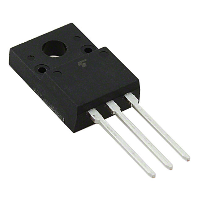
2SK4196LS N-Channel MOSFET 500V 5.5A Equivalent & Substitute Parts
Part Overview
The 2SK4196LS is an N-Channel MOSFET manufactured by onsemi, rated for 500V drain-to-source voltage with 5.5A continuous drain current at 25°C. The device is housed in a TO-220FI(LS) through-hole package and is classified as obsolete. Due to its obsolete status, equivalent and substitute parts from active product lines are necessary for ongoing design support and procurement continuity. Substitute devices maintain functional compatibility through matching or superior electrical ratings and identical through-hole mounting configuration.
Substiute Parts
Key Parameters
| Parameter | 2SK4196LS Value | Unit |
|---|---|---|
| FET Type | N-Channel | — |
| Technology | MOSFET (Metal Oxide) | — |
| Drain to Source Voltage (Vdss) | 500 | V |
| Current - Continuous Drain (Id) @ 25°C | 5.5 | A |
| Drive Voltage (Max Rds On) | 10 | V |
| Rds On (Max) @ Id, Vgs | 1.56 @ 2.8A, 10V | Ohm |
| Vgs(th) (Max) @ Id | 5 @ 1mA | V |
| Gate Charge (Qg) (Max) @ Vgs | 14.6 @ 10V | nC |
| Vgs (Max) | ±30 | V |
| Input Capacitance (Ciss) (Max) @ Vds | 360 @ 30V | pF |
| Power Dissipation (Max) | 2W (Ta), 30W (Tc) | W |
| Operating Temperature (TJ) | 150 | °C |
| Mounting Type | Through Hole | — |
| Package / Case | TO-220-3 Full Pack | — |
| Product Status | Obsolete | — |
Substitute Part Grouping Explanation
Substitute parts for the 2SK4196LS are selected based on the following critical electrical and mechanical parameters:
Primary Substitution Criteria:
- FET Type: N-Channel MOSFET (Metal Oxide technology)
- Drain-to-Source Voltage (Vdss): Equal to or greater than 500V
- Continuous Drain Current (Id) @ 25°C: Equal to or greater than 5.5A
- Drive Voltage: 10V gate drive compatibility
- Mounting Type: Through-hole configuration
- Package: TO-220-3 form factor
Secondary Compatibility Parameters:
- Gate threshold voltage (Vgs(th)): Within ±30V maximum gate voltage specification
- On-state resistance (Rds On): Lower or equivalent values ensure thermal performance
- Gate charge (Qg): Lower values reduce switching losses
- Input capacitance (Ciss): Affects gate drive requirements
- Power dissipation: Minimum 30W (Tc) rating for thermal management
All substitute parts listed maintain N-Channel MOSFET topology with through-hole TO-220 mounting. Toshiba π-MOSVII series devices provide active product status with RoHS3 compliance, addressing the obsolescence of the original 2SK4196LS component.
Parameter Comparison
| Parameter | 2SK4196LS | TK4A53D | TK5A45DA | TK5A50D | TK5A53D | TK5A55D | TK6A55DA | Unit |
|---|---|---|---|---|---|---|---|---|
| Drain to Source Voltage (Vdss) | 500 | 525 | 450 | 500 | 525 | 550 | 550 | V |
| Current - Continuous Drain (Id) @ 25°C | 5.5 | 4 | 4.5 | 5 | 5 | 5 | 5.5 | A |
| Rds On (Max) @ Id, Vgs | 1.56 @ 2.8A, 10V | 1.7 @ 2A, 10V | 1.75 @ 2.3A, 10V | 1.5 @ 2.5A, 10V | 1.5 @ 2.5A, 10V | 1.7 @ 2.5A, 10V | 1.48 @ 2.8A, 10V | Ohm |
| Vgs(th) (Max) @ Id | 5 @ 1mA | 4.4 @ 1mA | 4.4 @ 1mA | 4.4 @ 1mA | 4.4 @ 1mA | 4.4 @ 1mA | 4.4 @ 1mA | V |
| Gate Charge (Qg) (Max) @ Vgs | 14.6 @ 10V | 11 @ 10V | 9 @ 10V | 11 @ 10V | 11 @ 10V | 11 @ 10V | 12 @ 10V | nC |
| Input Capacitance (Ciss) (Max) @ Vds | 360 @ 30V | 490 @ 25V | 380 @ 25V | 490 @ 25V | 540 @ 25V | 540 @ 25V | 600 @ 25V | pF |
| Power Dissipation (Max) | 2W (Ta), 30W (Tc) | 35W (Tc) | 30W (Tc) | 35W (Tc) | 35W (Tc) | 35W (Tc) | 35W (Tc) | W |
| Operating Temperature (TJ) | 150 | 150 | 150 | 150 | 150 | 150 | 150 | °C |
| Mounting Type | Through Hole | Through Hole | Through Hole | Through Hole | Through Hole | Through Hole | Through Hole | — |
| Package / Case | TO-220-3 | TO-220-3 | TO-220-3 | TO-220-3 | TO-220-3 | TO-220-3 | TO-220-3 | — |
| Product Status | Obsolete | Active | Active | Active | Active | Active | Active | — |
Engineering Selection Recommendations
Primary Substitute: TK6A55DA(STA4,Q,M)
The TK6A55DA provides the closest electrical match to the 2SK4196LS with identical 5.5A continuous drain current rating and superior 550V Vdss specification. This device offers equivalent on-state resistance (1.48Ohm) and maintains the same gate drive voltage requirement. The TK6A55DA is manufactured by Toshiba Semiconductor and Storage with active product status and RoHS3 compliance, ensuring long-term availability and regulatory conformance.
Secondary Substitutes:
TK5A50D(STA4,Q,M) and TK5A53D(STA4,Q,M) provide suitable alternatives with 5A continuous drain current and 500V or 525V Vdss ratings respectively. Both devices feature improved on-state resistance (1.5Ohm) and reduced gate charge (11nC), resulting in lower switching losses compared to the original 2SK4196LS. These devices are available in high inventory quantities (12,300 and 921 units respectively) and carry RoHS3 compliance.
TK5A45DA(STA4,Q,M) is suitable for applications where 4.5A drain current is acceptable with 450V Vdss rating. This device exhibits the lowest gate charge (9nC) among all substitutes, reducing gate drive power requirements.
TK5A55D(STA4,Q,M) and TK4A53D(STA4,Q,M) provide higher voltage ratings (550V and 525V respectively) for applications requiring enhanced voltage margin, though with reduced drain current capabilities (5A and 4A respectively).
All substitute devices maintain through-hole TO-220-3 mounting compatibility and 150°C maximum junction temperature operation. Selection should be based on specific application requirements for drain current, voltage rating, and thermal dissipation capacity.
Frequently Asked Questions (FAQ)
Q: Can TK6A55DA(STA4,Q,M) directly replace 2SK4196LS in existing PCB designs?
A: Yes. The TK6A55DA maintains identical TO-220-3 through-hole pinout and footprint compatibility. Electrical specifications meet or exceed the 2SK4196LS requirements with 5.5A continuous drain current and 550V Vdss rating. No PCB modifications are required.
Q: What is the difference between TO-220FI(LS) and TO-220SIS packages?
A: Both are TO-220-3 form factor through-hole packages with identical lead spacing and mounting hole dimensions. The FI(LS) and SIS designations indicate manufacturer-specific package variants from onsemi and Toshiba respectively. Mechanical compatibility is maintained for PCB assembly.
Q: Why do substitute parts have lower gate charge (Qg) values?
A: Lower gate charge reduces the energy required to switch the MOSFET on and off, resulting in decreased switching losses and improved efficiency. This is a beneficial characteristic that does not affect substitution compatibility.
Q: Is the higher input capacitance (Ciss) of substitute parts a concern?
A: Input capacitance affects gate drive circuit design but does not prevent substitution. Higher Ciss values require slightly more gate drive current but remain compatible with standard 10V gate drive circuits. Gate drive circuit verification is recommended for high-frequency switching applications.
Q: Which substitute part has the best thermal performance?
A: TK6A55DA, TK5A50D, TK5A53D, and TK5A55D all feature 35W (Tc) power dissipation rating, compared to 30W (Tc) for the 2SK4196LS. This represents improved thermal capability. TK5A45DA maintains 30W (Tc) rating equivalent to the original device.
Q: Are all substitute parts RoHS compliant?
A: Yes. All Toshiba π-MOSVII series substitute parts carry RoHS3 compliance certification, meeting current environmental and regulatory requirements. The original 2SK4196LS does not specify RoHS status.
Q: What is the inventory status of substitute parts?
A: TK5A50D has the highest availability with 12,300 units in stock. TK5A45DA has 910 units, TK6A55DA has 1,025 units, TK5A53D has 921 units, TK5A55D has 1,048 units, and TK4A53D has 633 units available. All parts are listed as new original stock.
Q: Can I use TK5A45DA if my application only requires 4.5A drain current?
A: Yes. TK5A45DA is suitable for applications with 4.5A or lower drain current requirements. The 450V Vdss rating is lower than the 2SK4196LS, so voltage margin must be verified for your specific application. This device offers the lowest gate charge (9nC) among all substitutes.
Q: What is the significance of the π-MOSVII series designation?
A: π-MOSVII is the Toshiba product series classification for these high-voltage N-Channel MOSFETs. This designation indicates the device family and manufacturing process technology. All substitute parts from this series maintain consistent electrical characteristics and quality standards.
Alternative Parts

SJ6012L2TP
Littelfuse Inc.
6 Alternative Parts

JMK107BBJ476MA-RE
Taiyo Yuden
10 Alternative Parts

GMK107BBJ475MA-T
Taiyo Yuden
5 Alternative Parts
SJ6020N2ARP
Littelfuse Inc.
3 Alternative Parts
SJ6025R2ATP
Littelfuse Inc.
4 Alternative Parts

2474-05L
API Delevan Inc.
1 Alternative Parts

4590R-684K
API Delevan Inc.
1 Alternative Parts

CM6560R-334
API Delevan Inc.
1 Alternative Parts

CM6460-104
API Delevan Inc.
1 Alternative Parts

5526-12
API Delevan Inc.
1 Alternative Parts