


Request Quote
(Ships tomorrow)
2N5551 Equivalent & Substitute Parts
Part Overview
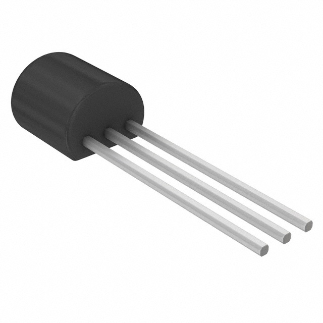
The 2N5551 is an NPN bipolar junction transistor manufactured by onsemi, designed for general-purpose switching and amplification applications. The device features a maximum collector current of 600 mA, collector-emitter breakdown voltage of 160 V, and maximum power dissipation of 625 mW in a through-hole TO-92 package. The 2N5551 is classified as obsolete, indicating that direct procurement from original manufacturing channels may be limited. Identifying equivalent and substitute parts ensures design continuity and maintains access to functionally compatible components for new production runs, repairs, and legacy system support.
Substiute Parts
Key Parameters
| Parameter | Value | Unit |
|---|---|---|
| Transistor Type | NPN | — |
| Current - Collector (Ic) (Max) | 600 | mA |
| Voltage - Collector Emitter Breakdown (Max) | 160 | V |
| Vce Saturation (Max) @ Ib, Ic | 200 mV @ 5 mA, 50 mA | — |
| Current - Collector Cutoff (Max) | 50 | nA |
| DC Current Gain (hFE) (Min) @ Ic, Vce | 80 @ 10 mA, 5 V | — |
| Power - Max | 625 | mW |
| Frequency - Transition | 300 | MHz |
| Operating Temperature | -55 to 150 | °C |
| Mounting Type | Through Hole | — |
| Package / Case | TO-92-3 (TO-226) | — |
Substitute Part Grouping Explanation
Substitution of the 2N5551 is determined by electrical and mechanical compatibility across the following critical parameters:
Electrical Compatibility Criteria:
- Transistor type must be NPN
- Maximum collector current (Ic) must equal or exceed 600 mA
- Collector-emitter breakdown voltage (VCEO) must equal or exceed 160 V
- Vce saturation characteristics must match or be superior (≤ 200 mV @ specified conditions)
- DC current gain (hFE) minimum must be ≥ 80 @ 10 mA, 5 V
- Maximum power dissipation must support 625 mW or greater
- Operating temperature range must encompass -55°C to 150°C
Mechanical Compatibility Criteria:
- Mounting type must be through-hole for direct PCB replacement
- Package must be TO-92-3 or equivalent footprint
Substitute parts are classified into two categories:
Direct Substitutes (Pin-Compatible, Through-Hole): Parts that maintain identical electrical specifications and through-hole TO-92-3 packaging, enabling direct board-level replacement without design modification.
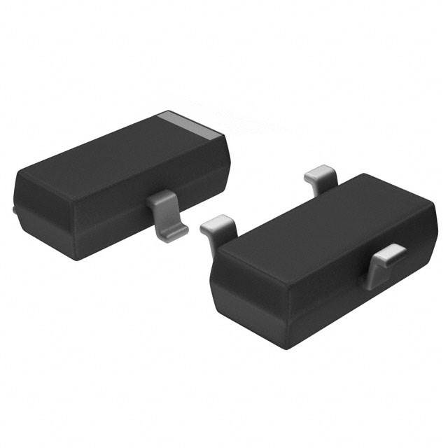
Functional Equivalents (Different Package): Parts that meet all electrical specifications but employ surface-mount packaging (SOT-23), requiring PCB layout and assembly process changes but offering equivalent electrical performance.
Parameter Comparison
| Parameter | 2N5551 | 2N5551BU | 2N5551YBU | MMBT5551_R1_00001 |
|---|---|---|---|---|
| Manufacturer | onsemi | onsemi | onsemi | Panjit International Inc. |
| Transistor Type | NPN | NPN | NPN | NPN |
| Current - Collector (Ic) (Max) | 600 mA | 600 mA | 600 mA | 600 mA |
| Voltage - Collector Emitter Breakdown (Max) | 160 V | 160 V | 160 V | 160 V |
| Vce Saturation (Max) @ Ib, Ic | 200 mV @ 5 mA, 50 mA | 200 mV @ 5 mA, 50 mA | 200 mV @ 5 mA, 50 mA | 200 mV @ 5 mA, 50 mA |
| Current - Collector Cutoff (Max) | 50 nA | 50 nA | Not specified | 50 nA |
| DC Current Gain (hFE) (Min) @ Ic, Vce | 80 @ 10 mA, 5 V | 80 @ 10 mA, 5 V | 180 @ 10 mA, 5 V | 80 @ 10 mA, 5 V |
| Power - Max | 625 mW | 625 mW | 625 mW | 250 mW |
| Frequency - Transition | 300 MHz | 100 MHz | 100 MHz | 300 MHz |
| Operating Temperature | -55 to 150 °C | -55 to 150 °C | -55 to 150 °C | -55 to 150 °C |
| Mounting Type | Through Hole | Through Hole | Through Hole | Surface Mount |
| Package / Case | TO-92-3 | TO-92-3 | TO-92-3 | SOT-23 |
| Product Status | Obsolete | Active | Active | Active |
| RoHS Status | Non-compliant | ROHS3 Compliant | ROHS3 Compliant | ROHS3 Compliant |
Engineering Selection Recommendations
For Direct Through-Hole Replacement (No PCB Redesign):
The 2N5551BU and 2N5551YBU are active-status direct substitutes for the obsolete 2N5551. Both parts maintain identical electrical specifications for collector current, breakdown voltage, saturation voltage, and operating temperature range. Both are manufactured by onsemi and packaged in TO-92-3, enabling pin-compatible board-level replacement.
The 2N5551BU operates at 100 MHz transition frequency compared to the original 300 MHz specification. This reduced frequency response is acceptable for applications where the original 300 MHz specification was not a critical design requirement.
The 2N5551YBU provides a higher DC current gain (hFE minimum of 180 @ 10 mA, 5 V) compared to the original specification (80 @ 10 mA, 5 V). This enhanced gain characteristic is compatible with existing designs and may improve circuit performance in gain-dependent applications.
Both 2N5551BU and 2N5551YBU carry ROHS3 compliance certification, addressing regulatory requirements for new production and commercial applications.
For Surface-Mount Implementation (PCB Redesign Required):
The MMBT5551_R1_00001 manufactured by Panjit International Inc. provides functional equivalence with identical electrical specifications for collector current, breakdown voltage, saturation voltage, and operating temperature. This part maintains the original 300 MHz transition frequency specification.
The MMBT5551_R1_00001 is packaged in SOT-23 surface-mount format, requiring PCB layout modification and surface-mount assembly processes. The maximum power dissipation is specified at 250 mW, which is lower than the original 625 mW specification. This reduced power rating requires thermal analysis to confirm suitability for applications approaching the original power dissipation limits.
The MMBT5551_R1_00001 carries ROHS3 compliance certification and is currently in active production status.
Frequently Asked Questions (FAQ)
Q: Can the 2N5551BU directly replace the 2N5551 on existing PCBs?
A: Yes. The 2N5551BU is pin-compatible with the 2N5551, sharing identical TO-92-3 through-hole packaging and footprint. No PCB modification is required for direct substitution. Electrical specifications for collector current (600 mA), breakdown voltage (160 V), saturation voltage (200 mV), and operating temperature range (-55 to 150°C) are identical.
Q: What is the difference between 2N5551BU and 2N5551YBU?
A: Both parts are pin-compatible through-hole substitutes with identical maximum ratings. The primary difference is DC current gain: 2N5551BU specifies a minimum hFE of 80 @ 10 mA, 5 V, while 2N5551YBU specifies a minimum hFE of 180 @ 10 mA, 5 V. The higher gain of the 2N5551YBU may provide improved performance in gain-dependent circuits. Both are ROHS3 compliant and in active production.
Q: Why does the MMBT5551_R1_00001 have lower power dissipation (250 mW vs. 625 mW)?
A: The MMBT5551_R1_00001 is a surface-mount SOT-23 package variant. The reduced power rating reflects the thermal characteristics of the smaller surface-mount package compared to the through-hole TO-92-3 package. Applications requiring sustained power dissipation near 625 mW must be evaluated for thermal compatibility with the 250 mW rating.
Q: Can the MMBT5551_R1_00001 be used as a direct replacement on existing PCBs?
A: No. The MMBT5551_R1_00001 uses SOT-23 surface-mount packaging, which has a different footprint than the through-hole TO-92-3 package. PCB layout redesign and surface-mount assembly processes are required. However, electrical specifications are compatible with the original 2N5551 design.
Q: Are all substitute parts RoHS compliant?
A: The original 2N5551 is RoHS non-compliant. Both 2N5551BU and 2N5551YBU are ROHS3 compliant, as is the MMBT5551_R1_00001. For applications requiring RoHS compliance, any of the three substitute parts satisfy regulatory requirements.
Q: What is the significance of the 300 MHz vs. 100 MHz transition frequency difference?
A: The original 2N5551 and MMBT5551_R1_00001 specify 300 MHz transition frequency. The 2N5551BU and 2N5551YBU specify 100 MHz. For switching applications operating well below 100 MHz, this difference is not significant. For high-frequency applications approaching or exceeding 100 MHz, the original 300 MHz specification or the MMBT5551_R1_00001 should be selected.
Q: Is the higher hFE of the 2N5551YBU (180 vs. 80) a problem for existing designs?
A: No. Higher DC current gain is compatible with existing designs. Circuits designed for minimum hFE of 80 will function correctly with a device providing minimum hFE of 180. The higher gain may reduce base current requirements and improve circuit efficiency in gain-dependent applications.
Alternative Parts

SJ6012L2TP
Littelfuse Inc.
6 Alternative Parts

JMK107BBJ476MA-RE
Taiyo Yuden
10 Alternative Parts

GMK107BBJ475MA-T
Taiyo Yuden
5 Alternative Parts
SJ6020N2ARP
Littelfuse Inc.
3 Alternative Parts
SJ6025R2ATP
Littelfuse Inc.
4 Alternative Parts

2474-05L
API Delevan Inc.
1 Alternative Parts

4590R-684K
API Delevan Inc.
1 Alternative Parts

CM6560R-334
API Delevan Inc.
1 Alternative Parts

CM6460-104
API Delevan Inc.
1 Alternative Parts

5526-12
API Delevan Inc.
1 Alternative Parts