


Request Quote
(Ships tomorrow)
2N5089TFR Equivalent & Substitute Parts
Part Overview
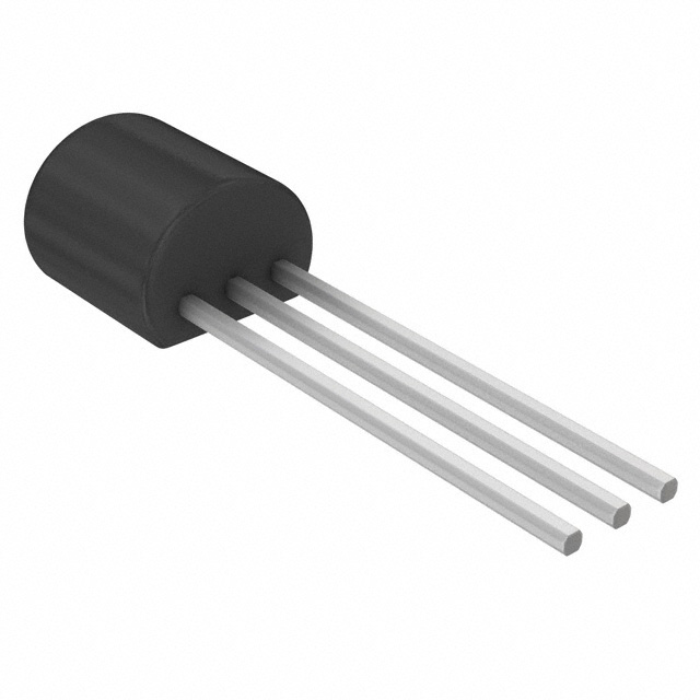
The 2N5089TFR is an NPN bipolar junction transistor manufactured by onsemi, designed for general-purpose switching and amplification applications. This device features a maximum collector current of 100 mA, collector-emitter breakdown voltage of 25 V, and maximum power dissipation of 625 mW in a Through Hole TO-92-3 package. The 2N5089TFR is classified as obsolete, making identification of suitable substitute components necessary for ongoing design support and production continuity. Equivalent parts must maintain functional compatibility within the specified electrical and mechanical parameters while accommodating modern component availability and compliance requirements.
Substiute Parts
Key Parameters
| Parameter | Value | Unit |
|---|---|---|
| Transistor Type | NPN | — |
| Current - Collector (Ic) Max | 100 | mA |
| Voltage - Collector Emitter Breakdown (Max) | 25 | V |
| Vce Saturation (Max) | 500 mV @ 1 mA, 10 mA | — |
| DC Current Gain (hFE) Min | 400 @ 100 µA, 5 V | — |
| Power - Max | 625 | mW |
| Frequency - Transition | 50 | MHz |
| Operating Temperature | -55 to 150 | °C |
| Mounting Type | Through Hole | — |
| Package / Case | TO-92-3 | — |
Substitute Part Grouping Explanation
Substitution of the 2N5089TFR is determined by compatibility across the following critical parameters:
Transistor Configuration: Both the main part and substitute must be NPN-type bipolar junction transistors to maintain circuit polarity and biasing requirements.
Electrical Ratings: Substitute parts must meet or exceed the collector current rating (100 mA minimum), collector-emitter breakdown voltage (25 V minimum), and power dissipation capability (625 mW minimum). Substitutes with higher ratings provide design margin and are acceptable for direct replacement.
Saturation Characteristics: Vce saturation voltage must be compatible with circuit switching requirements. Lower saturation voltages indicate improved switching performance.
Current Gain: DC current gain (hFE) specifications must support the intended biasing and amplification functions. Substitutes with different hFE values require circuit verification but do not preclude substitution if other parameters align.
Frequency Response: Transition frequency (fT) determines high-frequency performance capability. Substitutes with higher fT values provide enhanced frequency response.
Package and Mounting: The TO-92-3 Through Hole package is the standard form factor. Substitutes must use identical or mechanically compatible packaging to ensure PCB layout compatibility.
Temperature Range: Operating temperature range of -55°C to 150°C must be maintained or exceeded.
The 2N3904BU meets all substitution criteria with enhanced electrical performance characteristics and active product status.
Parameter Comparison
| Parameter | 2N5089TFR | 2N3904BU | Unit |
|---|---|---|---|
| Transistor Type | NPN | NPN | — |
| Current - Collector (Ic) Max | 100 | 200 | mA |
| Voltage - Collector Emitter Breakdown (Max) | 25 | 40 | V |
| Vce Saturation (Max) | 500 mV @ 1 mA, 10 mA | 300 mV @ 5 mA, 50 mA | — |
| Power - Max | 625 | 625 | mW |
| Frequency - Transition | 50 | 300 | MHz |
| Operating Temperature | -55 to 150 | -55 to 150 | °C |
| Mounting Type | Through Hole | Through Hole | — |
| Package / Case | TO-92-3 | TO-92-3 | — |
Engineering Selection Recommendations
2N3904BU as Primary Substitute
The 2N3904BU is a direct functional substitute for the 2N5089TFR. This device provides superior electrical performance across all critical parameters while maintaining identical package form factor and thermal operating range.
The 2N3904BU offers doubled collector current capacity (200 mA versus 100 mA), increased collector-emitter breakdown voltage (40 V versus 25 V), and significantly enhanced transition frequency (300 MHz versus 50 MHz). These enhanced ratings provide design margin and support higher-frequency applications without circuit modification.
The 2N3904BU is classified as Active product status, ensuring long-term availability and supply chain continuity. This device carries ROHS3 compliance certification, meeting current environmental and regulatory requirements. Both devices maintain identical REACH Unaffected status and EAR99 export classification.
The lower saturation voltage of the 2N3904BU (300 mV at 5 mA, 50 mA versus 500 mV at 1 mA, 10 mA) indicates improved switching efficiency and reduced power dissipation in saturation mode operation.
Pin-for-pin compatibility and identical TO-92-3 package geometry enable direct PCB substitution without layout modification. No circuit redesign is required for applications operating within the 2N5089TFR electrical envelope.
Frequently Asked Questions (FAQ)
Q: Can the 2N3904BU directly replace the 2N5089TFR without circuit modification?
A: Yes. The 2N3904BU is pin-for-pin compatible and maintains identical TO-92-3 package geometry. All electrical parameters of the 2N3904BU meet or exceed the 2N5089TFR specifications. Direct substitution is supported for applications operating within the original design envelope.
Q: What are the key differences between these devices?
A: The 2N3904BU provides enhanced performance: doubled collector current capacity (200 mA versus 100 mA), higher breakdown voltage (40 V versus 25 V), and six-fold increase in transition frequency (300 MHz versus 50 MHz). The 2N3904BU also exhibits lower saturation voltage, indicating improved switching characteristics. These enhancements provide design margin without introducing compatibility issues.
Q: Why is the 2N5089TFR classified as obsolete?
A: The 2N5089TFR is listed as obsolete by the manufacturer. The 2N3904BU represents the modern equivalent, offering superior performance and active product status with guaranteed long-term availability.
Q: Are there package compatibility concerns?
A: No. Both devices use the TO-92-3 Through Hole package with identical lead configuration and spacing. PCB layouts designed for the 2N5089TFR accommodate the 2N3904BU without modification.
Q: Does the higher transition frequency of the 2N3904BU affect low-frequency applications?
A: No. Higher transition frequency does not degrade performance in low-frequency or DC applications. The enhanced frequency response of the 2N3904BU provides additional capability without affecting operation in the original application bandwidth.
Q: What compliance certifications apply to the 2N3904BU?
A: The 2N3904BU is ROHS3 compliant and maintains REACH Unaffected status. Both devices share identical EAR99 export classification. The 2N3904BU meets current environmental and regulatory requirements for commercial and industrial applications.
Q: Is circuit biasing adjustment necessary when substituting the 2N3904BU?
A: No circuit biasing adjustment is required. The 2N3904BU operates within the same voltage and current ranges as the 2N5089TFR. Existing bias networks and component values remain valid for direct substitution.
Alternative Parts

SJ6012L2TP
Littelfuse Inc.
6 Alternative Parts

JMK107BBJ476MA-RE
Taiyo Yuden
10 Alternative Parts

GMK107BBJ475MA-T
Taiyo Yuden
5 Alternative Parts
SJ6020N2ARP
Littelfuse Inc.
3 Alternative Parts
SJ6025R2ATP
Littelfuse Inc.
4 Alternative Parts

2474-05L
API Delevan Inc.
1 Alternative Parts

4590R-684K
API Delevan Inc.
1 Alternative Parts

CM6560R-334
API Delevan Inc.
1 Alternative Parts

CM6460-104
API Delevan Inc.
1 Alternative Parts

5526-12
API Delevan Inc.
1 Alternative Parts