


Request Quote
(Ships tomorrow)
Equivalent & Substitute Parts for Renesas 271PGILF
Part Overview
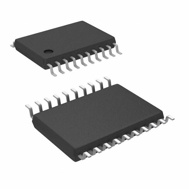
The Renesas 271PGILF is a Clock/Frequency Synthesizer and Fanout Buffer (Distribution) IC operating at up to 200MHz in a 20-TSSOP surface mount package. This component is classified as obsolete, making identification of functionally equivalent alternatives essential for ongoing system support and new design implementations. The part features integrated PLL with bypass capability, crystal input, and CMOS output configuration suitable for clock distribution applications.
Substiute Parts
Key Parameters
| Parameter | Specification |
|---|---|
| Manufacturer Part Number | 271PGILF |
| Manufacturer | Renesas Electronics Corporation |
| Category | Clock/Timing |
| Type | Clock/Frequency Synthesizer, Fanout Buffer (Distribution) |
| Package / Case | 20-TSSOP (0.173", 4.40mm Width) |
| Frequency - Max | 200MHz |
| Voltage - Supply | 3.135V ~ 3.465V |
| Operating Temperature | -40°C ~ 85°C |
| PLL | Yes with Bypass |
| Input Type | Crystal |
| Output Type | CMOS |
| Ratio - Input:Output | 1:6 |
| Divider/Multiplier | Yes/Yes |
| Mounting Type | Surface Mount |
| Product Status | Obsolete |
Substitute Part Grouping Explanation
Substitution of the 271PGILF is determined by strict alignment of the following critical parameters:
Package Compatibility: Both the main part and substitute must use the 20-TSSOP (0.173", 4.40mm Width) surface mount package to ensure PCB footprint compatibility without layout redesign.
Functional Architecture: The substitute must provide Clock/Frequency Synthesizer functionality with integrated PLL and bypass capability, crystal input support, and CMOS output configuration.
Electrical Performance: The substitute must support the 1:6 input-to-output ratio, include divider and multiplier functionality, and operate within the -40°C to 85°C temperature range.
Supply Voltage: The substitute operating voltage range must be compatible with or encompass the 3.135V to 3.465V specification of the original part.
Maximum Frequency: The substitute maximum frequency specification must meet or exceed 200MHz to maintain system timing requirements.
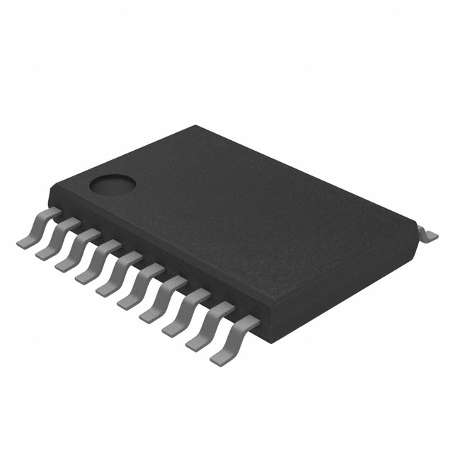
The Texas Instruments CDCE706PW meets all substitution criteria through identical package geometry, equivalent functional architecture, compatible electrical specifications, and active product status.
Parameter Comparison
| Parameter | Renesas 271PGILF | Texas Instruments CDCE706PW | Compatibility |
|---|---|---|---|
| Manufacturer Part Number | 271PGILF | CDCE706PW | Different manufacturers |
| Package / Case | 20-TSSOP (0.173", 4.40mm Width) | 20-TSSOP (0.173", 4.40mm Width) | Identical |
| Type | Clock/Frequency Synthesizer, Fanout Buffer | PLL Frequency Synthesizer | Functionally equivalent |
| PLL | Yes with Bypass | Yes with Bypass | Identical |
| Input Type | Crystal | LVCMOS, Crystal | Compatible (CDCE706PW supports additional input types) |
| Output Type | CMOS | LVCMOS | Compatible (LVCMOS is CMOS-compatible) |
| Ratio - Input:Output | 1:6 | 1:6 | Identical |
| Divider/Multiplier | Yes/Yes | Yes/Yes | Identical |
| Frequency - Max | 200MHz | 300MHz | Compatible (CDCE706PW exceeds requirement) |
| Voltage - Supply | 3.135V ~ 3.465V | 3V ~ 3.6V | Compatible (ranges overlap) |
| Operating Temperature | -40°C ~ 85°C | -40°C ~ 85°C | Identical |
| Mounting Type | Surface Mount | Surface Mount | Identical |
| Product Status | Obsolete | Active | Substitute is actively manufactured |
| Number of Circuits | 1 | 1 | Identical |
Engineering Selection Recommendations
The Texas Instruments CDCE706PW is the qualified substitute for the Renesas 271PGILF based on the following engineering criteria:
Package Equivalence: Both components use the identical 20-TSSOP surface mount package, eliminating PCB redesign requirements and ensuring direct footprint compatibility.
Functional Parity: The CDCE706PW provides equivalent Clock/Frequency Synthesizer functionality with PLL and bypass capability, matching the core architecture of the 271PGILF.
Electrical Compatibility: The CDCE706PW operates within compatible voltage ranges (3V to 3.6V encompasses the 3.135V to 3.465V specification) and maintains the same operating temperature range (-40°C to 85°C).
Performance Enhancement: The CDCE706PW maximum frequency specification of 300MHz exceeds the 200MHz requirement, providing additional performance margin.
Product Availability: The CDCE706PW maintains active product status with verified programmability and RoHS3 compliance, ensuring long-term supply chain stability and regulatory alignment.
Regulatory Compliance: Both components share identical REACH status (REACH Unaffected) and ECCN classification (EAR99), maintaining consistent export and compliance documentation.
Frequently Asked Questions (FAQ)
Q: Can the CDCE706PW be used as a direct replacement for the 271PGILF without PCB modifications?
A: Yes. Both components use the 20-TSSOP package with identical pin pitch and body dimensions. Direct footprint substitution is possible without PCB layout changes.
Q: Are the input and output signal types compatible between these parts?
A: Yes. The 271PGILF accepts crystal input and provides CMOS output. The CDCE706PW accepts crystal input (plus additional LVCMOS input options) and provides LVCMOS output, which is electrically compatible with CMOS specifications.
Q: What is the significance of the 300MHz maximum frequency on the CDCE706PW compared to the 200MHz specification of the 271PGILF?
A: The higher maximum frequency specification on the CDCE706PW provides additional performance headroom. For applications requiring 200MHz operation, the CDCE706PW operates well within its rated specifications, ensuring reliable performance.
Q: Are the supply voltage ranges compatible?
A: The voltage ranges are compatible. The 271PGILF operates at 3.135V to 3.465V, and the CDCE706PW operates at 3V to 3.6V. The overlapping range (3.135V to 3.465V) ensures compatible operation in existing power supply designs.
Q: Does the CDCE706PW support the same 1:6 input-to-output ratio?
A: Yes. Both components support the 1:6 input-to-output ratio and include divider and multiplier functionality for flexible clock distribution configurations.
Q: What is the impact of the 271PGILF being obsolete?
A: The obsolete status of the 271PGILF indicates that Renesas has discontinued manufacturing. The CDCE706PW, with active product status, ensures continued availability for new designs and system maintenance.
Q: Are there any programming or configuration differences between these parts?
A: The CDCE706PW is verified as programmable through DiGi-Electronics, while the 271PGILF programmability status is not verified. Consult the respective datasheets for detailed programming interface specifications and configuration procedures.
Alternative Parts

SJ6012L2TP
Littelfuse Inc.
6 Alternative Parts

JMK107BBJ476MA-RE
Taiyo Yuden
10 Alternative Parts

GMK107BBJ475MA-T
Taiyo Yuden
5 Alternative Parts
SJ6020N2ARP
Littelfuse Inc.
3 Alternative Parts
SJ6025R2ATP
Littelfuse Inc.
4 Alternative Parts

2474-05L
API Delevan Inc.
1 Alternative Parts

4590R-684K
API Delevan Inc.
1 Alternative Parts

CM6560R-334
API Delevan Inc.
1 Alternative Parts

CM6460-104
API Delevan Inc.
1 Alternative Parts

5526-12
API Delevan Inc.
1 Alternative Parts