


Request Quote
(Ships tomorrow)
Renesas 2510CG Clock Driver IC Equivalent & Substitute Parts
Part Overview
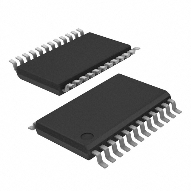
The Renesas 2510CG is a Clock Driver, Fanout Distribution, Spread Spectrum Clock Generator IC rated for 175MHz operation in a 24-TSSOP surface mount package. This part is classified as Obsolete, making equivalent and substitute parts necessary for ongoing design support and procurement. The 2510CG provides PLL-based clock distribution with a 1:10 input-to-output ratio, CMOS output, and operates across a 2.97V to 3.63V supply range.
Substiute Parts
Key Parameters
| Parameter | Value |
|---|---|
| Manufacturer | Renesas Electronics Corporation |
| Part Number | 2510CG |
| Product Category | Clock Driver, Fanout Distribution, Spread Spectrum Clock Generator |
| Package Type | 24-TSSOP (0.173", 4.40mm Width) |
| Mounting Type | Surface Mount |
| PLL Configuration | Yes with Bypass |
| Input Type | Clock |
| Output Type | CMOS |
| Number of Circuits | 1 |
| Input:Output Ratio | 1:10 |
| Maximum Frequency | 175MHz |
| Supply Voltage Range | 2.97V ~ 3.63V |
| Operating Temperature | 0°C ~ 70°C |
| RoHS Status | RoHS non-compliant |
| Moisture Sensitivity Level | 1 (Unlimited) |
| Product Status | Obsolete |
Substitute Part Grouping Explanation
Substitution of the Renesas 2510CG is determined by the following critical parameters:
Package Compatibility: All substitute parts must use the 24-TSSOP (0.173", 4.40mm Width) surface mount package to ensure PCB footprint compatibility.
PLL Architecture: All substitutes maintain PLL with Bypass configuration, ensuring functional equivalence in clock distribution applications.
Frequency Rating: Substitute parts are grouped into two frequency classes: 125MHz maximum (CDC2510 series) and 175MHz maximum (CDCVF2510 series). The 175MHz-rated substitutes provide direct frequency compatibility with the 2510CG.
Supply Voltage: All substitutes operate within 3V to 3.6V range, which overlaps with the 2510CG's 2.97V to 3.63V specification.
Input/Output Characteristics: The CDC2510 series maintains 1:10 ratio with Clock input and Clock output. The CDCVF2510 series operates at 2:11 ratio with LVTTL input and LVTTL output, representing a functional alternative for applications tolerating different signal levels and ratios.
Number of Circuits: All substitutes provide single-circuit configuration matching the 2510CG.
Parameter Comparison
| Parameter | 2510CG (Renesas) | CDC2510BPWR (TI) | CDC2510CPW (TI) | CDC2510CPWR (TI) | CDCVF2510APW (TI) | CDCVF2510APWR (TI) | CDCVF2510PW (TI) | CDCVF2510PWR (TI) |
|---|---|---|---|---|---|---|---|---|
| Manufacturer | Renesas | Texas Instruments | Texas Instruments | Texas Instruments | Texas Instruments | Texas Instruments | Texas Instruments | Texas Instruments |
| Package Type | 24-TSSOP | 24-TSSOP | 24-TSSOP | 24-TSSOP | 24-TSSOP | 24-TSSOP | 24-TSSOP | 24-TSSOP |
| PLL with Bypass | Yes | Yes | Yes | Yes | Yes | Yes | Yes | Yes |
| Number of Circuits | 1 | 1 | 1 | 1 | 1 | 1 | 1 | 1 |
| Maximum Frequency | 175MHz | 125MHz | 125MHz | 125MHz | 175MHz | 175MHz | 175MHz | 175MHz |
| Input:Output Ratio | 1:10 | 1:10 | 1:10 | 1:10 | 2:11 | 2:11 | 2:11 | 2:11 |
| Input Type | Clock | Clock | Clock | Clock | LVTTL | LVTTL | LVTTL | LVTTL |
| Output Type | CMOS | Clock | Clock | Clock | LVTTL | LVTTL | LVTTL | LVTTL |
| Supply Voltage Range | 2.97V ~ 3.63V | 3V ~ 3.6V | 3V ~ 3.6V | 3V ~ 3.6V | 3V ~ 3.6V | 3V ~ 3.6V | 3V ~ 3.6V | 3V ~ 3.6V |
| Operating Temperature | 0°C ~ 70°C | 0°C ~ 70°C | 0°C ~ 85°C | 0°C ~ 85°C | 0°C ~ 85°C | 0°C ~ 85°C | 0°C ~ 85°C | 0°C ~ 85°C |
| RoHS Status | RoHS non-compliant | ROHS3 Compliant | ROHS3 Compliant | ROHS3 Compliant | ROHS3 Compliant | ROHS3 Compliant | ROHS3 Compliant | ROHS3 Compliant |
| Product Status | Obsolete | Not For New Designs | Not For New Designs | Not For New Designs | Active | Active | Active | Active |
| Moisture Sensitivity Level | 1 (Unlimited) | 1 (Unlimited) | 1 (Unlimited) | 1 (Unlimited) | 1 (Unlimited) | 1 (Unlimited) | 1 (Unlimited) | 1 (Unlimited) |
Engineering Selection Recommendations
For Direct Frequency and Ratio Compatibility (175MHz, 1:10): The Renesas 2510CG has no direct equivalent among the Texas Instruments substitutes. The CDCVF2510 series (CDCVF2510APW, CDCVF2510APWR, CDCVF2510PW, CDCVF2510PWR) operates at 175MHz but uses a 2:11 ratio with LVTTL input/output instead of 1:10 CMOS. These parts are suitable only if the application can accommodate the different ratio and signal levels.
For Frequency Downgrade Tolerance (125MHz, 1:10): The CDC2510 series (CDC2510BPWR, CDC2510CPW, CDC2510CPWR) provides 1:10 ratio matching with Clock input/output, but operates at a maximum of 125MHz. These parts are suitable for applications where 125MHz operation is acceptable and the lower frequency requirement is not a constraint.
For New Designs: The CDCVF2510 series parts (CDCVF2510APW, CDCVF2510APWR, CDCVF2510PW, CDCVF2510PWR) carry Active product status and ROHS3 compliance, making them the preferred choice for new designs. CDC2510 series parts are marked "Not For New Designs" and should be avoided in new applications.
For Extended Temperature Range: CDC2510CPW, CDC2510CPWR, and all CDCVF2510 variants support 0°C to 85°C operation, exceeding the 2510CG's 0°C to 70°C range.
For RoHS Compliance: All Texas Instruments substitutes are ROHS3 compliant, whereas the Renesas 2510CG is RoHS non-compliant.
Frequently Asked Questions (FAQ)
Q: Can CDC2510BPWR, CDC2510CPW, or CDC2510CPWR directly replace the Renesas 2510CG?
A: These parts share the same 24-TSSOP package, PLL with Bypass configuration, 1:10 ratio, and Clock input/output type. However, they are limited to 125MHz maximum frequency compared to the 2510CG's 175MHz rating. Substitution is valid only if your application operates at or below 125MHz.
Q: What is the difference between CDC2510 and CDCVF2510 series?
A: The CDC2510 series maintains a 1:10 input-to-output ratio with Clock input and Clock output. The CDCVF2510 series operates at a 2:11 ratio with LVTTL input and LVTTL output. The CDCVF2510 series supports 175MHz operation matching the 2510CG frequency, but the different ratio and signal levels require circuit-level evaluation.
Q: Why are some CDC2510 parts marked "Not For New Designs"?
A: CDC2510BPWR, CDC2510CPW, and CDC2510CPWR carry this designation indicating they are legacy products. For new designs, select from the CDCVF2510 series (CDCVF2510APW, CDCVF2510APWR, CDCVF2510PW, CDCVF2510PWR), which are all Active status parts.
Q: Does packaging type affect substitution?
A: All substitute parts use the same 24-TSSOP surface mount package. Packaging variants (Tube, Tape & Reel) do not affect electrical compatibility, only procurement and handling logistics.
Q: Are all substitutes RoHS compliant?
A: Yes. All Texas Instruments substitutes are ROHS3 compliant. The original Renesas 2510CG is RoHS non-compliant. If RoHS compliance is required, any Texas Instruments substitute satisfies this requirement.
Q: What is the operating temperature difference?
A: The Renesas 2510CG operates 0°C to 70°C. CDC2510 and CDCVF2510 series parts operate 0°C to 85°C, providing a 15°C extended upper temperature range.
Q: Can I use CDCVF2510PWR in place of the 2510CG?
A: CDCVF2510PWR matches the 175MHz frequency rating and maintains PLL with Bypass architecture in the same 24-TSSOP package. However, the 2:11 ratio and LVTTL signal levels differ from the 2510CG's 1:10 ratio and CMOS output. Substitution requires verification that downstream circuitry can accept LVTTL levels and operate with the 2:11 ratio.
Alternative Parts

SJ6012L2TP
Littelfuse Inc.
6 Alternative Parts

JMK107BBJ476MA-RE
Taiyo Yuden
10 Alternative Parts

GMK107BBJ475MA-T
Taiyo Yuden
5 Alternative Parts
SJ6020N2ARP
Littelfuse Inc.
3 Alternative Parts
SJ6025R2ATP
Littelfuse Inc.
4 Alternative Parts

2474-05L
API Delevan Inc.
1 Alternative Parts

4590R-684K
API Delevan Inc.
1 Alternative Parts

CM6560R-334
API Delevan Inc.
1 Alternative Parts

CM6460-104
API Delevan Inc.
1 Alternative Parts

5526-12
API Delevan Inc.
1 Alternative Parts