 >
>


Product Overview: VIPER50A STMicroelectronics Primary Switch Mode Power Supply IC
The VIPER50A from STMicroelectronics represents a sophisticated solution within the domain of primary switch-mode power supply ICs, purpose-built for off-line flyback topologies. Leveraging integrated VIPower M10 process technology, this device unifies advanced PWM control circuits with a high-voltage, avalanche-rugged vertical power MOSFET. This monolithic integration reduces component count, minimizes parasitics, and shortens loop lengths, directly translating to enhanced EMI performance and improved conversion efficiency in compact system footprints.
At the heart of the design is the high-voltage MOSFET rated for either 620V or 700V and a pulse capability of 1.5A. This high ruggedness supports direct connection to rectified AC mains without the need for bulky external passive elements often required for voltage withstand, thus realizing PCB-level miniaturization in universal input designs. The robust avalanche capability ensures resilience in the face of switching and line surges, offering enhanced operational reliability in environments with frequent voltage transients or noisy mains—conditions typical in industrial automation, white goods, and appliance power modules.
By integrating PWM control, startup circuitry, and protection functions, the VIPER50A eliminates the need for discrete controller ICs, drivers, and HV startup resistors. This level of integration not only streamlines BOM cost and layout complexity but also enables stable soft-start operation, over-temperature and overload safeguarding, and cycle-by-cycle current limitation—features essential for long-term field reliability. In practical low-power, offline flyback designs, such as LED drivers, smart metering, or auxiliary supplies for larger SMPS, designers often encounter thermal limitations and efficiency ceilings below 25–50W. The VIPER50A provides consistent switching characteristics to maintain high conversion efficiency across a wide-range input and output spectrum while supporting both wide-range (up to 25W) and single-range/doubler (up to 50W) topologies.
In real-world applications, especially where PCB real estate is at a premium, the 5-PENTAWATT package offers excellent thermal dissipation and straightforward assembly. Its compact footprint addresses the miniaturization imperatives found in emerging IoT power nodes, standby bias sources, and fast-charging adapters.
With the flexibility to operate directly from AC lines and deliver robust power conversion for a variety of SMPS topologies, this IC allows engineers to accelerate development cycles and mitigate risks associated with power stage overstress. The integration level reflects a strategic transition in primary-side power design—from traditional discrete assemblies toward system-level, IC-based approaches favoring reliability, scalability, and mass production efficiency. A subtle but notable insight is the reliability assurance under pulse stresses: the avalanche energy absorption characteristic not only shields downstream components but also opens the field for aggressive primary-side filter and snubber design, potentially reducing overall system cost while maintaining regulatory compliance.
Through careful thermal management, proper snubber selection, and attention to PCB creepage and clearance for primary-mains safety, power supply designs based on VIPER50A can fulfill stringent EMI, standby, and safety standards. This device, therefore, occupies a vital niche as both a platform for rapid productization and a resilient solution for markets valuing high integration, efficient thermal handling, and fail-safe operation under challenging line conditions.
Key Features and Functional Advantages of VIPER50A
VIPER50A integrates a comprehensive suite of features, each aligned with the requirements of modern power supply architecture. The adjustable switching frequency, extendable up to 200 kHz, enables designers to optimize EMI performance, transformer sizing, and transient response based on specific converter demands. Fine-tuning the switching rate makes it practical to balance conversion efficiency against physical footprint and magnetic component saturation, facilitating tailored designs for both dense industrial controllers and large commercial equipment.
Underlying control is managed via a current-mode topology, which inherently streamlines loop compensation and provides rapid response to input voltage fluctuations. This structure simplifies stabilization in demanding environments, reducing susceptibility to line disturbances and improving overall accuracy. Current-mode regulation also supports inherent pulse-by-pulse current limiting, enhancing protection against overload conditions and improving fault tolerance in intricate multi-rail systems.
VIPER50A leverages embedded soft start and shutdown mechanisms, which orchestrate gradual ramp-up of output voltage to minimize electrical stress on downstream components during power sequencing. This gentle excitation regime mitigates risks of capacitor charge surges and semiconductor overstress, especially when integrating with sensitive logic sections or analog front-ends. The device’s controlled shutdown path permits orderly system deactivation, crucial for maintaining data integrity and process safety in automation networks.
Automated burst mode transition during stand-by operation maximizes idle energy savings, ensuring sub-1 watt consumption and enabling full compliance with eco-design directives such as “Blue Angel.” The seamless shift to burst mode, without requiring external logic intervention, allows robust standby management in distributed platforms, extending product lifecycle and optimizing operational expenses. Implementing this feature has demonstrated marked reductions in standby losses during qualification phases, directly contributing to thermal management goals in enclosed installations.
For precision output regulation, an internally trimmed Zener acts as a stable reference, supporting tight voltage tolerance across temperature and process drift variances. Such integrated referencing eliminates the need for costly external precision components, streamlining BOM and calibration procedures. Designers have observed a notable improvement in system voltage accuracy and reproducibility, directly impacting yield in high-volume manufacturing.
The undervoltage lock-out with hysteresis is engineered to avert erratic start-up behavior and brown-out vulnerabilities. By incorporating controlled hysteresis thresholds, the device prevents inadvertent toggling during marginal supply conditions, thereby safeguarding software initialization routines and reducing false error triggers in mission-critical control loops.
Built-in startup supply circuitry reduces external discretization, simplifying PCB design and improving overall manufacturability. This feature is especially beneficial in tight layouts where component count and reliability are primary concerns. Experience shows that the reduction in external circuitry expedites prototyping and lowers maintenance intervention rates.
Avalanche ruggedness and snubberless operation further bolster robustness, particularly in low-power designs subjected to inductive switching and grid-side transients. The device’s capacity to withstand repetitive surge events without external snubber networks translates into enhanced long-term durability and minimized board complexity, which is valued in field-deployed automation panels and remote monitoring units.
Integrated overtemperature protection ensures the converter remains within defined thermal parameters, dynamically shutting down and recycling operation when excessive junction temperatures are detected. Coupled with adjustable current limiting, this provides a configurable safety envelope for diverse load profiles, guarding against thermal runaways during overload scenarios or forced air cooling failures.
Low stand-by current, combined with the aforementioned features, positions VIPER50A as an optimal choice for developing high-efficiency switched-mode supplies. Strategically, the cohesive design philosophy—centered on integration, adaptability, and protection—supports reliable operation, accelerates time to market, and meets sustainability objectives in contemporary industrial and commercial power management.
VIPER50A System Architecture and Pin Description
The VIPER50A system exemplifies advanced integration by combining a high-voltage power MOSFET with a current-mode PWM controller on a single die. Central to its design is the internal SenseFET, which performs primary side current measurement with minimal propagation delay, enabling rapid overcurrent protection and cycle-by-cycle control accuracy. This approach reduces the latency typical in discrete implementations, supporting tight output regulation and robust fault response across varying load conditions.
Underlying mechanism foundation rests on precise current sensing and switching control. The Drain pin not only acts as the high-voltage entry point but also sources start-up bias via its intrinsic HV current source, supporting self-activation from bulk voltage rails common in offline converter topologies. During normal operation, the pin endures voltage stress from switching transients and manages unclamped energy, requiring careful PCB layout to minimize parasitic effects and ensure reliability. Experience shows that optimal trace routing and sufficient creepage distance are critical, particularly when leveraging the system in environments with surge requirements.
The Source pin establishes the low-side reference, tying the high-voltage switching MOSFET’s source to ground. Consistent ground referencing is vital to minimize noise coupling and ensure measurement integrity, especially when implementing EMI filters or handling complex power ground architectures in multi-rail systems.
For powering internal logic, the VDD pin accepts a wide input range, thanks to an integrated start-up current source, streamlining the auxiliary bias network often needed in legacy designs. This pin’s versatility becomes apparent when using feedback schemes based on optocouplers or auxiliary windings. The IC’s compatibility with both methods enables migration between isolation requirements without major redesign, a feature leveraged in rapid prototyping cycles and when scaling platforms for diverse line voltages.
Control loop and regulation depth emerge via the COMP pin, where the error amplifier’s output supports loop compensation and burst mode engagement. The pin’s dual role as a shut-down trigger, activated by pulling COMP low, naturally supports dynamic power management strategies—vital for meeting modern standby efficiency regulations. Implementations with capacitive coupling on the COMP node have demonstrated improved transient response and smoother transitions into low-power modes, particularly in flyback topologies aimed at consumer electronics.
Switching frequency manipulation is facilitated by the OSC pin. Connection to external RT and CT components provides granular adjustment to accommodate transformer characteristics, EMI compliance targets, and efficiency optimization. Synchronization to an external clock is also supported, which is beneficial for interleaved or frequency-spread applications, allowing coordinated system operation and minimized peak EMI emissions. Field deployment reveals that frequency synchronization delivers substantial benefits in multi-converter environments, enhancing system resilience against conducted and radiated disturbances.
System-level integration reduces external component count, streamlines power supply design, and promotes high functional density. This influences not only BOM cost but also thermal management and long-term system reliability. The architecture’s inherent support for dual feedback mechanisms and idle mode enhance flexibility, permitting deployment from low-wattage adapters to larger, isolated auxiliary supplies in industrial controls. The subtle interplay between the internal SenseFET and compensation logic yields remarkable control authority, helping to meet both regulation and efficiency thresholds without elaborate analog circuitry.
From a design perspective, leveraging the VIPER50A’s unified approach empowers rapid iteration and adaptability, especially when tailoring supplies to varying load profiles and regulatory scenarios. Its optimized pinout and deep system integration streamline electromagnetic compliance and increase tolerance to input surge events, while its modulation and feedback structures accelerate convergence in both isolated and non-isolated converter applications. Overall, the architecture stands out for enabling high-efficiency, low-footprint power solutions with robust regulation, minimal external circuitry, and reliable start-up even under challenging input conditions.
Electrical Performance and Operating Conditions of VIPER50A
Electrical performance of the VIPER50A is defined by precise internal thresholds and robust circuit integration, facilitating reliable operation across diverse power converter topologies. The device initiates start-up below 8V VDD; above 11V, internal references maintain operating points with tight regulation. This threshold design ensures that supply voltage fluctuations, common in flyback and buck-boost applications, are mitigated at the controller level, minimizing unpredictable start or stop behaviors even under significant line dips or transient conditions.
The switching frequency is established by the oscillator network on the OSC pin, leveraging a resistor-capacitor (RT-CT) pair. The architecture isolates frequency control from VDD instability, holding switching frequency steady across typical 8V–15V supply variations. This decoupling is critical in practice for maintaining EMI compliance and output ripple targets during brown-in or brown-out events. When targeting specific frequency bands, fine-tuning of RT and CT values allows precise adaptation to transformer design constraints and efficiency optimization goals.
Ruggedness is engineered into the device with a specified avalanche energy rating, protecting the integrated MOSFET under severe inductive overvoltage stress. This is indispensable in offline converters supplying motor drives, relays, or poorly damped transformer outputs, where repetitive fast switching events can induce high voltage transients. The device absorbs these surges without catastrophic failure, extending converter service life even with challenging field loads.
The current mode control topology not only stabilizes output under load transients but also provides natural current limiting during faults or start-up. The fast cycle-by-cycle current sense loop responds rapidly to abnormal events—such as transformer saturation or secondary side shorts—preventing extended stress on the power switch and magnetic components. This approach supports robust protection without excessive shutdown interruptions, a characteristic observed in demanding industrial environments with variable loads.
Integrated blanking circuitry filters noise and transformer ringing, suppressing false tripping of the pulse termination mechanism. In practical circuit layouts where gate-drive or sense traces pick up switching artifacts, this feature ensures that noise does not prematurely end conduction cycles, thereby maximizing energy delivery and avoiding erratic regulation. Dimensioning the blanking interval provides an effective compromise between fast fault response and operational stability, especially when paired with oversized magnetics or PCB layouts with aggressive parasitic coupling.
The error amplifier's 1.5 mA/V typical transconductance enables robust loop gain while offering flexibility in compensation schemes. Designers can tailor the external feedback network for either bandwidth maximization—critical for rapid transient recovery—or for soft-start behavior, where gradual rise in output minimizes stress on downstream circuits and prevents inrush currents. Real-world tuning often invokes a staggered compensation pole-zero network to manage phase margin without sacrificing load regulation, underscoring the value of accessible compensation pin architecture.
Integrated feature synergy—start-up logic, oscillator independence, current mode limitation, noise rejection, and flexible feedback—establishes the VIPER50A as a reliable platform for compact, high-performance offline switchers. Progressive optimization of these aspects in application-specific prototypes consistently demonstrates enhanced power density, fault tolerance, and ease of compliance with regulatory standards. Such an approach enables both rapid design iterations and robust deployment in environments where predictable performance remains paramount.
Application Guidance for VIPER50A in Off-Line Power Supplies
For off-line power conversion across auxiliary power units, industrial controllers, and consumer electronics, VIPER50A delivers an adaptable topology for applications demanding 25W to 50W of regulated output. Its architecture accommodates both primary-side and secondary-side regulation, supporting flexible transformer design and enabling designers to select control schemes that best match isolation and feedback requirements. Such versatility directly addresses the mixed needs of single- and dual-output converter stages frequently encountered in modular electronics, automation panels, and low-to-mid power embedded systems.
The integrated burst mode stands out in low-load scenarios, executing output regulation while reducing switching losses and magnetic bias currents. This function consistently achieves sub-watt stand-by performance, addressing regulatory constraints prevalent in energy-saving contexts without sacrificing cold-start reliability or output stability. Practical deployment reveals that fine-tuning burst mode thresholds can balance stand-by efficiency against wake-up response, offering granular control for differing end-use profiles.
External component selection significantly impacts start-up reliability, switching frequency control, and feedback integrity. The VDD capacitor value governs the IC’s ability to withstand brown-out and transient conditions; optimal sizing ensures robust supply hold during line dips and repetitive start-up cycles under variable loads. The RT-CT network on the OSC pin directly defines switching frequency, influencing transformer core selection, EMI profile, and efficiency curves. Strategic selection of timing elements not only minimizes operating losses but also enables easy adaptation to market-standard emission requirements and noise-sensitive industrial deployments.
The device’s slope compensation circuitry is activated in continuous conduction mode to suppress subharmonic oscillations during high-duty operation, making it suitable for converters operated above 50% duty cycle and supporting output ripple minimization. Deployment in multi-rail topologies leverages external clock synchronization, facilitating phase-aligned operation across interconnected power modules, which enhances overall system EMI performance and harmonizes load sequencing. Experience indicates that clock integrity and PCB layout play vital roles in synchronization success, with ground plane management and trace routing becoming decisive factors in large-scale system integration.
VIPER50A's ability to bridge advanced regulation methods with robust protective features, such as integrated current limiting and thermal shutdown, streamlines compliance with industrial reliability standards. Such convergence empowers engineering teams to accelerate design cycles while maintaining a strong foundation for both longevity and flexibility in rapidly evolving electronic platforms. This approach capitalizes on the compact integration of control logic and protection circuitry, reducing BOM complexity and mitigating risk in field deployments.
Protection, Robustness, and Reliability Features of VIPER50A
The VIPER50A integrates a suite of protection and reliability mechanisms that collectively enable sustained performance in power conversion systems subject to diverse operational disturbances. The device’s overtemperature safeguard is triggered at a minimum junction threshold of 140°C, leveraging an internal thermal shutdown circuit. Recovery is autonomous, with operation resuming only after a substantial thermal differential (at least 40°C below trip-point). This margin not only shields critical die areas from cumulative thermal stress, but also ensures that the device does not oscillate, reinforcing long-term reliability in environments with fluctuating cooling conditions or transient over-power scenarios.
At a systemic level, the undervoltage lockout embedded in the VIPER50A directly manages bias conditions. Upon detecting voltage below a set minimum, the controller executes an orderly shutdown. This approach prevents erratic switching activity, securing both the switch-mode power supply and the downstream circuitry from undervoltage-induced startup malfunctions, which can otherwise result in load misbehavior or permanent converter damage. The lockout mechanism operates autonomously, contributing to predictable system response in brown-out or power restoration events—a key factor during grid disturbances or battery discharge cycles.
Current-mode control within the device serves a dual function: output regulation and protection. The architecture restricts peak current during overload and short-circuit faults, temporarily reducing switch duty cycle and preventing catastrophic MOSFET stress. Once fault conditions abate, automatic restoration is enacted without external intervention. This design eliminates downtime and simplifies fault recovery, advantageous in electrically noisy environments or installations with intermittent load profiles.
In addressing power stage robustness, the VIPER50A’s avalanche-rated MOSFET mitigates voltage spike transients that often accompany inductive load switching or transformer flyback scenarios. The absence of a discrete snubber network—a result of avalanche capability—reduces PCB component count and simplifies assembly layout, facilitating both compact converter topologies and improved manufacturability. This snubberless approach is particularly beneficial in high-density or isolated applications, where board space is at a premium and the avoidance of parasitic effects is critical.
Surge resilience is further elevated by provision for an external RC filter at the VDD pin. While intrinsic circuit design imparts strong noise immunity, supplemental filtering enables tailored response to transformer-coupled impulsive events, such as lightning or switching surges. Correctly dimensioned RC networks have proved effective in field deployments, attenuating voltage noise without impairing converter startup timing or normal operation. In practical terms, surge conditioning at the bias pin has yielded extended operational lifespans across installations exposed to variable power quality.
A cohesive view of these features reveals a device engineered for high-integrity operation across a spectrum of electrical stresses. The integration of self-recovering protective algorithms, robust switching elements, and scalable external conditioning options, when combined with carefully matched system architecture, supports sustainable converter up-time and minimizes service intervals. In tightly regulated applications—such as industrial control, consumer SMPS, or transport power supplies—this approach enables design prioritization toward simplicity, reliability, and long-term cost reduction.
PCB Layout Considerations for VIPER50A Designs
PCB layout for VIPER50A-based power conversion systems demands rigorous attention to both signal integrity and electromagnetic compatibility. The primary switching loop, which carries pulsed high currents, must be optimized by minimizing enclosed areas. This directly reduces loop inductance, a key generator of radiated emissions and switching noise, thereby supporting compliance with stringent EMI standards. In practice, this optimization is achieved through tight coupling of traces between the VIPER50A’s switching pins, transformer primary terminals, and associated snubber networks. Employing wide and short traces for these paths further suppresses voltage spikes caused by fast transients.
Careful segregation of signal domains is fundamental. Traces carrying high di/dt switching currents must be physically distanced and electrically isolated from analog or control signal traces. This spatial and layer-level separation prevents capacitive or inductive coupling that can corrupt low-level measurement or reference signals. Ground return paths should be partitioned: power and signal grounds are kept distinct except for a single star ground point, typically near the IC, to avert ground loops—an approach validated in high-reliability industrial controls.
Placement of decoupling capacitors warrants particular scrutiny. For the VIPER50A, ceramic capacitors with low ESR and ESL characteristics should be mounted with minimal lead or trace length, directly adjoining the relevant supply and reference pins. When supporting transformer windings, capacitors must shunt high-frequency disturbances immediately at the transformer's foot, intercepting noise before it propagates through the board. Experience shows that such proximity yields lower overshoot and reduced susceptibility to conducted interference.
Operational robustness in demanding environments further hinges on strategic via placement and the use of uninterrupted copper planes beneath fast-switching sections. Multi-layer boards with dedicated ground and power planes enhance both thermal dissipation and EMI shielding. Isolated transformer layouts and layout symmetry mitigate the risk of parasitic oscillations, especially in wide-input systems typical of industrial automation.
A refined approach incorporates layout simulations prior to fabrication, leveraging tools for electromagnetic field analysis and validating design choices against real-world switching waveforms. Such preemptive validation consistently aligns field performance with design objectives and exposes latent coupling issues early in development. This methodology, tightly coupled with empirical measurement post-assembly, establishes a feedback cycle for continuous improvement, distinguishing resilient VIPER50A applications in variable industrial contexts.
Distinctive value arises from iterative layout enhancement, where lessons from operational anomalies inform subsequent routing and component placement strategies. The convergence of simulation, measurement, and physical design ensures each iteration yields quantifiable reductions in EMI and boosts long-term system reliability, characterizing the optimal deployment of VIPER50A devices in critical power delivery roles.
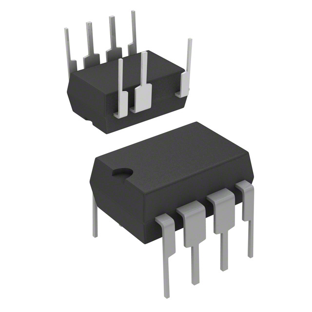
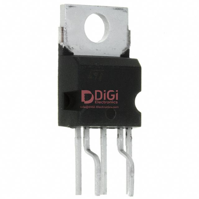
Mechanical and Packaging Information for VIPER50A
The VIPER50A integrates seamlessly into various designs by leveraging two established package formats: PENTAWATT and PowerSO-10. These packages are engineered to support robust heat dissipation and electrical integrity, essential for high-power switching applications. The PENTAWATT package, with its expanded lead pitch and exposed pad geometry, facilitates direct heat transfer to the PCB copper area, significantly reducing junction temperatures during sustained operation. PowerSO-10 further advances thermal management by offering a large cooling surface and optimized lead configuration, enabling compact layouts while maintaining low parasitic resistance and inductance.
Precise pad layout guidance enhances the IC’s operational stability. Designers are encouraged to maximize copper-bearing areas beneath the package pads, utilizing thermal vias to connect to inner or rear PCB layers where necessary. This approach distributes thermal flux, minimizing hotspots and keeping the device within safe limits under varying load conditions. Electrical performance gains are achieved by maintaining short, wide traces for high-current outputs and careful routing of sensitive signal pins to reduce crosstalk. Such layout practices have demonstrated substantial improvements in delivered output power and signal fidelity, particularly in densely populated power supply boards.
Manufacturing logistics are streamlined via support for both tube and tape-and-reel shipments. This adaptability enables automated placement and rapid assembly line integration across diverse production scales. Tube packaging mitigates handling-specific damage for prototyping or low-volume batches, while tape-and-reel options allow high-speed pick-and-place operations, reducing turnaround time and lowering defect rates during mass manufacturing. Attention to device orientation and mechanical alignment during placement has a direct impact on yields, especially when working with thermally enhanced leadframes.
A noteworthy design consideration lies in the synergy between packaging geometry and board-level thermal design. Selecting the optimal package—PENTAWATT for larger, high-thermal mass assemblies or PowerSO-10 for dense layouts—can elevate product reliability and operational headroom. Multilayer PCB designs that exploit these thermal paths often unlock higher performance thresholds, enabling aggressive derating curves and extended lifetime projections. This interdependence of mechanical, thermal, and electrical strategies underscores a broader trend toward holistic system-level optimization, where packaging details have a measurable effect on the overall efficiency and endurance of power converters using the VIPER50A device.
Potential Equivalent/Replacement Models for VIPER50A
The VIPER50A series from STMicroelectronics operates at the intersection of high-voltage power conversion and robust system integration. When device availability is constrained or when a design calls for enhanced integration or improved efficiency, evaluation of closely related variants is both strategic and necessary. The baseline VIPER50 model preserves the essential topology and operating envelope characteristic of the VIPER50A, including similar voltage and current handling, integrated PWM control, and start-up circuitry. This reference compatibility ensures minimal deviation in PCB layout and system reliability, favoring rapid migration in time-sensitive redesigns.
Further differentiation exists in the VIPER50SP and VIPER50ASP derivatives. These options cater to diverse packaging requirements—such as through-hole versus SMD configuration—which can significantly affect thermal dissipation pathways and mechanical stability under continuous load. Slight adjustments in their electrical specifications, such as maximum switching frequency, MOSFET voltage tolerance, and thermal resistance, provide vital handles for tuning the design towards higher performance or lower BOM cost, depending on project priorities.
Detailed cross-comparison forms the core of a robust replacement process. It is essential to methodically map application needs—including switching behavior, peak loading profiles, inrush current characteristics, and EMI constraints—against datasheet parameters of each candidate device. For example, when migrating a flyback converter topology, the chosen replacement must not only meet the breakdown voltage requirements but also maintain loop response fidelity across the designated operating frequency. Experience shows that a nuanced review of control flexibility—such as options for programmable soft-start or adjustable current limiting—streamlines optimization for end-product reliability.
Integrating these findings into practice, designers typically adopt a layered validation approach, beginning with simulation under worst-case loading, followed by prototyping with real components to monitor thermal profiles in situ. Effective thermal management, informed by packaging selection, often yields marginal performance improvements, particularly in restricted enclosure designs. Notably, in high-density applications, leveraging SMD variants provides substantial footprint reduction at the cost of careful heat sinking strategies, while through-hole options offer easier power dissipation but necessitate more board space.
Through iterative refinement, the final device choice is shaped by a convergence of electrical compatibility, mechanical fit, and holistic system efficiency. A subtle but significant insight is that tight alignment between application-driven specifications and device capabilities—not simply direct parameter matching—determines long-term reliability and compliance. This approach unearths advantageous synergies, such as exploiting thermal margin to enable silent operation or using enhanced control features for adaptive load management.
By progressing methodically from core mechanism awareness to context-driven selection, engineers build resilient, scalable power conversion solutions optimized for present and future challenges.
Conclusion
VIPER50A from STMicroelectronics serves as a consolidated solution for primary switch mode power supply (SMPS) architectures in off-line environments, merging power conversion, control logic, and protection mechanisms into a single package. At its core, the device integrates a high-voltage vertical power MOSFET with dedicated control circuitry, leveraging advanced silicon processes and system-level optimization to minimize parasitics and thermal losses. This integration not only streamlines board-level complexity—by reducing the need for discrete driver stages and auxiliary components—but also facilitates tighter regulation and faster transient response in demanding load conditions.
The on-chip protection features extend beyond conventional overvoltage and overcurrent safeguards, incorporating input undervoltage lockout, thermal shutdown, and soft-start functionalities. These capabilities are engineered to maintain system integrity under abnormal operational states and abrupt line disturbances, thus enhancing long-term reliability in environments subject to voltage sags or spikes. The embedded circuitry’s high switching efficiency, achieved through low gate charge and optimized clamp transitions, directly benefits energy-sensitive applications where standby consumption and thermal budget are tightly specified.
In deployment, the VIPER50A simplifies both procurement and assembly. Its high integration mitigates sourcing risks for discrete parts, reducing bill-of-material line counts and manufacturing variability. PCB layout benefits from minimized critical paths and simplified grounding schemes, allowing for more compact power stages without compromising electromagnetic compatibility. Design iterations can focus on fine-tuning transformer size, EMI filtering, and loop compensation, rather than troubleshooting basic power conversion anomalies.
Real-world implementations across industrial controllers, smart appliances, and building automation systems consistently demonstrate stable performance with low cycle-to-cycle jitter and consistent startup even under wide input voltage ranges. Selection and configuration parameters, such as external feedback network values or snubber optimization, play a decisive role in maximizing power density and reliability. Proactively balancing switching frequency and thermal dissipation ensures the system remains within lifetime targets, especially in high-duty industrial settings.
Ultimately, the VIPER50A embodies the transition towards unified power platforms where enhanced functional density and intrinsic protection improve both cost-effectiveness and system robustness. This approach unlocks new design flexibility in competitive power conversion markets, encouraging streamlined workflows and robust product portfolios.