


 >
>


Product overview of VIPER35LD STMicroelectronics IC OFFLINE SWITCH FLYBACK 16SO
The VIPER35LD by STMicroelectronics epitomizes the integration of advanced power conversion technology within a single IC, streamlining the design of off-line flyback converters. At its core, the device fuses an 800 V avalanche-rugged power MOSFET with a quasi-resonant current-mode PWM controller, orchestrated to achieve high efficiency and operational reliability in isolated power supply environments. This system-level approach not only minimizes external component requirements but also enables designers to achieve robust performance metrics within strict space and cost constraints.
Delving into its underlying mechanisms, the high-voltage MOSFET leverages a proprietary process for sustained avalanche ruggedness, ensuring intrinsic protection against line surges and transients—a common concern in AC mains applications. The integration of senseFET technology replaces conventional sense resistors, enabling cycle-by-cycle current monitoring with negligible power loss and enhanced system robustness. The PWM controller operates in quasi-resonant mode, dynamically adapting the switching frequency to the transformer’s magnetization state, thereby reducing switching losses, improving EMI behavior, and lowering core and MOSFET stress under varying load conditions. Soft-start implementation ensures controlled energy delivery at power-up, limiting inrush current and increasing the longevity of downstream components.
Protection features anchor the device’s reliability. The embedded HV start-up circuit drastically reduces standby losses by deactivating itself after initial power-up, outsourcing biasing to the auxiliary winding. This architectural decision allows the system to achieve sub-30 mW consumption at 230 VAC no-load, directly catering to stringent global energy efficiency regulations such as ErP Lot 6 and DOE Level VI. Comprehensive fault handling—including output overvoltage, secondary-side short-circuit detection, over-temperature protection with hysteresis, and a fault auto-restart mechanism—prevents catastrophic failures and supports higher system uptime. These protections are internally coordinated, eliminating the need for additional external circuitry and simplifying the qualification process in safety-critical or industrial-grade designs.
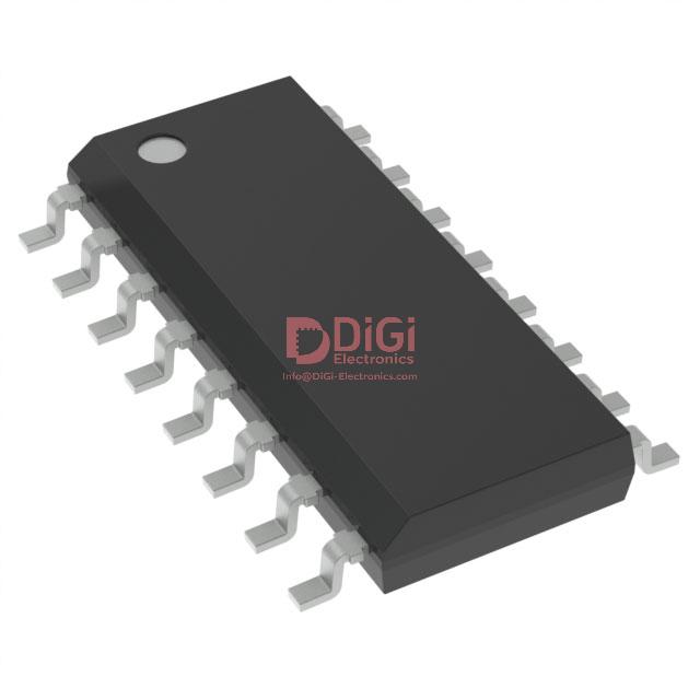
From a layout and assembly perspective, the availability in an SO16N package facilitates straightforward integration onto multi-layer PCBs, even in dense form factors such as adapter modules or embedded auxiliary power subassemblies. The standard footprint ensures compatibility with automated pick-and-place processes, supporting rapid prototyping and scaling to mass production without the need for custom enclosures.
Real-world applications showcase the VIPER35LD’s efficacy across diverse product segments. For instance, its burst-mode operation under light-load conditions proves instrumental in maintaining compliance with stringent standby power limits in consumer appliances, while the quasi-resonant scheme reduces audible noise—an often-overlooked attribute in contemporary home and office devices. In industrial control panels, its ruggedness, along with integrated protections and minimal external circuitry, results in expedited regulatory approval and reduced bill of materials, ultimately shrinking both time-to-market and total system costs. The device further distinguishes itself in embedded charger designs, where consistent thermal management is vital due to continuous high-load operation.
While the VIPER35LD embodies state-of-the-art advances in power IC consolidation, a nuanced engineering insight is its ability to balance system reliability with design agility. By encapsulating protection, efficiency, and control within a unified platform, it affords engineers the latitude to innovate at the application layer rather than expending resources on discrete power train optimization. This synergy between integration and adaptability marks a subtle but distinct shift in the development philosophy for compact, high-reliability power converters.
Typical output power specifications for VIPER35LD STMicroelectronics IC OFFLINE SWITCH FLYBACK 16SO
The output power characteristics of the VIPER35LD, an integrated offline flyback switch from STMicroelectronics, pivot on thermal interaction with the surrounding enclosure. When positioned within non-ventilated adapters at a 50°C ambient, the IC exhibits output power typical for compact charging circuits and auxiliary rails where heat dissipation is challenged by limited airflow. The proprietary thermal shutdown and power MOSFET integration within the VIPER35LD ensure that performance remains robust, albeit constrained by the enclosure's ability to channel heat away from sensitive components. Design choices must account for the maximal ambient temperature and restricted convection; thermal rise calculations and PCB copper area allocation for heat spreading become critical tools.
Transitioning to open-frame system layouts with adequate heatsinking, the situation shifts toward higher power throughput. Here, improved heat extraction elevates the feasible continuous power rating, enabling more demanding loads and longer operational duty cycles. Engineers routinely exploit open-frame designs for set-top boxes, industrial control units, and metering solutions, balancing output demands with cost and space constraints. Selection of heatsink geometry, attention to airflow direction, and optimization of PCB thermal pathways all serve to unlock greater utilization of the VIPER35LD. The device’s self-protection features allow for aggressive power envelope targeting, provided heat stress remains within the junction temperature limits.
The underlying mechanism driving these disparities in output performance is the relationship between junction temperature and external cooling environment. The converter’s switching efficiency, snubber loss, and the primary FET’s R_DS(on) all factor into the heat budget, reinforcing the necessity for system-level thermal simulation. Practically, experience shows that maximizing copper pour under the IC and ensuring tight thermal coupling to chassis parts can yield up to 20–30% improvement in output power versus minimalistic layouts. For high-reliability or tightly packed consumer adapters, a conservative power rating with strategic derating for worst-case temperatures extends field lifetime and suppresses early failure rates.
Application fit is determined not only by nominal output ratings but also by transient load behavior, regulation precision, and EMI constraints. For gaming adapters, the VIPER35LD’s soft-start and overvoltage protection features mitigate startup surges, supporting delicate device charging cycles. Metering and industrial loads benefit from the predictable shutdown response and broad input voltage range, securing device robustness under grid stress conditions. Design iterations reveal that integrating optimized snubber circuits and employing primary-side regulation yields both cleaner output and improved thermal stability.
Strategically, the device’s appropriateness is only fully realized when both electrical and thermal margins are factored into early-stage design verification, without assuming datasheet ratings translate directly into finished product capability. This approach, reinforced by iterative board prototyping and real-world temperature profiling, forms the bedrock of reliable system integration for the VIPER35LD in diverse roles.
Pin description for VIPER35LD STMicroelectronics IC OFFLINE SWITCH FLYBACK 16SO
STMicroelectronics’ VIPER35LD integrates advanced offline flyback switching features within a 16-pin SO package, where effective pinout utilization directly influences power conversion reliability and performance. The DRAIN pin plays a central role by connecting to both the high-voltage switching loop and the integrated HV start-up generator, combining power delivery and cold-start functions. An optimized layout ensures minimal parasitic induction during switching transients, which enhances efficiency and mitigates EMI issues.
The VDD pin receives supply voltage sourced from an auxiliary transformer winding, supporting both start-up and steady-state operation. Consistent VDD rail integrity is maintained through precise transformer turn ratios and decoupling choices, diminishing susceptibility to voltage sags that could trigger erratic switching or under-voltage lockout. This stability directly correlates with predictable MOSFET gate drive timing and safeguards controller autonomy against common-mode disturbances.
ZCD (Zero-Current Detection) constitutes a multi-domain diagnostic node. It governs valley switching for efficiency, enables adaptive current limit configuration, and provides fast feed-forward compensation to reject line voltage variation impacts. In well-engineered flyback converters, external resistor networks attached to ZCD set the detection threshold to balance quick load response with noise immunity. ZCD also monitors output via OVP (Over-Voltage Protection), automatically coordinating shut-down scenarios when thresholds are exceeded. This flexibility allows precise tailoring to end-system safety requirements without burdensome firmware overhead.
FB (Feedback) orchestrates primary-side regulation, modulating PWM signals and burst mode engagement, directly impacting output voltage quality and standby power. FB further acts as an OLP (Overload Protection) input, meaning resistor divider values and compensation capacitor selection influence both transient response and fault-handling accuracy. Subtle feedback loop tuning is often necessary to minimize overshoot during load jumps while preserving robust fault isolation, especially in complex multi-output topologies.
BR (Brown-Out) detection safeguards the converter against operating below safe input voltage thresholds by disconnecting switching during mains undervoltage events. This function relies on precise external resistor selection tailored for specific input AC profiles, preventing nuisance trips while guarding against hazardous regulation states. For installations with erratic grid conditions, judicious BR pin calibration maintains system uptime without sacrificing protection margins.
Ancillary pins in the VIPER35LD oversee core controller operation, manage logic sequencing, and implement system-level protections, such as soft-start and thermal shutdown. A disciplined routing strategy for control and sense lines minimizes crosstalk and enhances diagnostic robustness, especially under rapid load or voltage deviations.
Effective integration of VIPER35LD’s pinout hinges on a systems-level approach—balancing electrical characteristics with physical implementation to unlock high-efficiency, rugged, and adaptive flyback designs. Strategic resistor choices at ZCD and BR serve as the linchpin for intelligent control activation, enabling nuanced protection regimes and agile response profiles. Optimized pin-level configuration transforms the IC into a foundation for scalable offline switching architectures adaptable to both consumer and industrial voltage domains, reflecting a convergence of silicon advances and proven field design practices.
Absolute maximum ratings and thermal data for VIPER35LD STMicroelectronics IC OFFLINE SWITCH FLYBACK 16SO
When considering the VIPER35LD from STMicroelectronics, a robust appreciation of its absolute maximum ratings is foundational for reliable system design. The IC’s DRAIN terminal capability of withstanding voltages up to 800 V ensures compatibility with global mains inputs, tolerating transient overvoltages inherent in switch-mode power supply applications. This wide margin must be respected scrupulously, as even momentary excursions beyond this threshold can initiate avalanche breakdown or compromise dielectric integrity, precipitating irreversible device failure and system downtime. Careful attention to input filtering, surge protection, and layout geometry around high-voltage pins is essential here.
Thermal constraints converge at three principal metrics: maximum allowable junction temperature, storage temperature, and package power dissipation. Each functions as a guardrail within which the IC delivers predictable performance. Excessive junction temperature accelerates aging and degrades switching efficiency, so staying well beneath the manufacturer’s ceiling—even during sustained peak conditions—is critical. This is often achieved through aggregate thermal management techniques: limited copper pour on the PCB, strategic via arrays for heat spreading, and coordinated airflow routes. Storage temperature bounds guarantee that supply chain and device staging environments do not introduce latent reliability risks before deployment. Package power dissipation, a function of both switching losses and conduction characteristics, directly relates to external component selection and load profiles.
The junction-to-ambient (RθJA) and junction-to-case (RθJC) resistances, derived under controlled FR4 mounting with designated copper area, provide a basis for calculating temperature rise under load. Here, subtle variations in board stackup, solder pad coverage, solder quality, and mounting orientation present measurable impact. Designing with a conservative margin beyond theoretical calculations accounts for manufacturing tolerances and real-world installation. Observations from prototyped layouts highlight tangible differences in temperature profiles across copper areas—incremental increases in copper can suppress junction temperatures by several degrees, enhancing long-term stability.
Optimal deployment scenarios exploit the VIPER35LD’s ratings by harmonizing electrical parameters with thermal design. For flyback converter topologies, leveraging high DRAIN voltage resilience enables minimalist snubber selection and compact transformer designs, while meticulous thermal pathway engineering secures headroom for ambient temperature excursions. Effective PCB architecture—favoring short, broad traces between heat-generating nodes and thermal relief pads—proves critical, especially in dense systems or minimal airflow environments.
The key insight is that thermal and electrical margins are interlocked in practical applications; extending either margin independently without holistic design consideration yields suboptimal reliability. Balancing the VIPER35LD’s rugged voltage handling with advanced thermal dissipation strategies transforms potential stressors into design strengths. Proactive engagement with these parameters during layout and assembly, coupled with preemptive bench testing under worst-case conditions, establishes a foundation for dependable operation in demanding power conversion environments.
Electrical characteristics of VIPER35LD STMicroelectronics IC OFFLINE SWITCH FLYBACK 16SO
The VIPER35LD, a highly integrated offline flyback switch from STMicroelectronics, demonstrates a well-controlled electrical profile tailored for switched-mode power supply architectures. Its start-up and operational VDD thresholds are engineered to maintain repeatable power sequencing and minimize mis-triggering events, especially under wide input voltage ranges and variable load startups. The internal high-voltage circuitry precisely defines these thresholds, providing resilience against input line disturbances and gradual voltage ramp scenarios often encountered in industrial and consumer designs.
A critical aspect of operational robustness is the management of the drain current limit (IDlim). Here, the VIPER35LD dynamically adjusts its current limit with temperature, factoring in both silicon process variation and thermal rise. This is further refined through the Zero-Current Detection (ZCD) pin, enabling application-specific tuning. Such pin-level configurability supports both tight fault protection and performance optimization across mission profiles. Field experience shows that careful ZCD adjustment balances protection versus efficiency, especially in designs sensitive to peak power delivery or subject to frequent line surges.
The performance envelope of the internal MOSFET is largely dictated by RDS(on) and BVDSS responses to junction temperature. Lower RDS(on) values at typical operating points ensure reduced conduction losses, boosting conversion efficiency and easing thermal management requirements. The device’s BVDSS (drain-source breakdown voltage) margin, characterized over temperature, assures integrity in sudden overvoltage events or when driving high-voltage transformer primaries. Observing the evolution of RDS(on) with aging and soldering profiles can lead to more reliable pre-production qualification and long-term field reliability.
Power consumption patterns are engineered to scale efficiently from no-load to full-load conditions. The switching controller's quiescent current and gate-drive optimization deliver low standby power—essential for energy standards such as ErP Lot 6 or 10. By analyzing consumption trends under fluctuating line and load scenarios, designers can precisely model efficiency curves and thermal budgets, avoiding costly over-specification. Experience indicates that slight adjustments in external feedback components can yield significant gains in standby power without affecting dynamic performance.
Technical documentation provides granular tables and parametric graphs facilitating device selection and application alignment. Notably, accurate characteristic mapping enables iterative design refinement, aligning silicon behavior with system-level compliance for EMC, thermal, and safety benchmarks. The VIPER35LD exemplifies the interconnectedness of hardware-level parameter tuning and system reliability, reinforcing the notion that robust power conversion is both an art of detail and an exercise in systems engineering rigor.
Efficiency performance for typical flyback applications using VIPER35LD STMicroelectronics IC OFFLINE SWITCH FLYBACK 16SO
Efficiency performance for typical flyback applications utilizing the VIPER35LD IC from STMicroelectronics demonstrates a refined balance between switching operation and energy conservation. Central to offline flyback converter selection, energy efficiency represents not only regulatory compliance but also a direct contributor to system reliability and operating cost reduction. The VIPER35LD, integrated with robust high-voltage startup circuitry and a highly optimized control core, elevates efficiency across a broad load profile.
Measured across standard loading points—25%, 50%, 75%, and 100%—and under both 115 VAC and 230 VAC mains, the device adheres to the Energy Star active mode methodology. This protocol emphasizes weighted average efficiency, thus pushing converter solutions beyond simple maximum-load metrics. The architecture of the VIPER35LD minimizes losses in both conduction and switching via carefully orchestrated on-chip gate driving, snubberless operation, and adaptive switching frequency control. Additionally, burst-mode operation at lighter loads sharply reduces switching events per cycle, leading to extremely low standby power consumption. Observations in practical setups reveal total input power draw well within regulatory constraints, highlighting the IC’s ability to manage line transients and variable load while maintaining eco-design targets.
The layered approach in the VIPER35LD’s design integrates primary control, high-voltage startup, and advanced protection into a compact package, reducing BOM complexity and improving thermal management. For always-on and consumer electronics, such as routers, set-top boxes, or IoT hubs, this operational profile aligns with the demand for persistent connectivity without energy penalties. In deployment, the fast dynamic response and narrow line/load regulation window enable designers to avoid overdesign of transformer or secondary-side circuitry, translating into both system cost and efficiency gains.
One practical insight is derived from iterative prototyping and thermal cycling—heat-sink requirements can be reduced thanks to the converter’s reduced dissipation, particularly under light-load. Furthermore, the high integration density expedites PCB layout, reduces EMI fingerprint, and assists in passing global energy and safety certifications, which otherwise become bottlenecks in regulatory-driven time-to-market scenarios.
A nuanced observation is that the VIPER35LD’s efficiency benefits extend into shipment-stage logistics as well: products equipped with such power sections inherently score favorably in eco-labeling schemes, which is increasingly a criterion in consumer preference and permitted sales channels. The intersection of high efficiency, regulatory compliance, and topological flexibility makes the VIPER35LD a pivotal option for engineers pursuing stringent power, cost, and design envelope requirements in contemporary flyback applications.
Operation and control fundamentals of VIPER35LD STMicroelectronics IC OFFLINE SWITCH FLYBACK 16SO
VIPER35LD—an offline flyback switch from STMicroelectronics—embeds several finely engineered control functionalities that target robust, efficient power conversion across a broad range of auxiliary supply designs. At the foundational hardware level, the IC leverages an 800 V avalanche-rugged N-channel MOSFET utilizing senseFET architecture to achieve precise primary-side current sensing. This intrinsic topology minimizes layout parasitics, supporting reliable overcurrent protection and stable mode transition during dynamic loading. Engineering teams frequently optimize layout placement to further reduce sense signal interference, boosting measurement fidelity under noisy conditions.
Gate control integrates an EMI-conscious driver tailored to suppress voltage overshoots and mitigate both hard and soft switching artifacts, preserving switching integrity even under adverse input transients. Integrated UVLO functionality disables gate triggering below design thresholds, forcibly preventing unwanted conduction that may lead to system instability during brown-out scenarios. Voltage excursions or missing auxiliary voltage scenarios thus remain systematically controlled.
The high-voltage start-up generator operates as a discrete activation block, drawing current from the DRAIN above its turn-on threshold. This mechanism restricts initial VDD supply to brief intervals, handing over supply responsibility to the auxiliary winding once flyback operation stabilizes. In fast-cycle prototyping phases, this ensures reduced stress on startup circuit components, lengthening their operating lifetime and minimizing leakage paths. Transients associated with cold start—with previously discharged VDD—are characterized by deterministic voltage ramping, reducing spurious turn-on and cross-regulatory harmonics.
Soft-start logic is embedded to modulate rise times during converter enablement, thus tempering instantaneous current spikes through the secondary diode. This layer enhances transformer longevity, sidestepping temporary magnetic core saturation and related electromagnetic emission events. Applications employing sensitive output stages benefit from extended soft-start intervals, where iterative trial timings can help balance between minimal overshoot and optimal response speed.
Monotonic power-down orchestration drives controlled output collapse, addressing the frequent challenge of residual charge-induced restart attempts as input voltage declines. By managing deenergization precisely, the IC inhibits reactive re-triggering, which might otherwise complicate downstream circuitry or cause out-of-spec system states. Applied experience shows that setting decay constants according to load demands—rather than purely input capacitance—can further tailor system reliability in variable line conditions.
Auto-restart protocols initiated after fault diagnosis—including output short, line surge or overheating—initiate tailored VDD capacitor charging cycles, balancing between quick recovery and targeted protection. This avoids thermal overstress, supports regulatory fault metrics, and enhances converter resilience against repeated adverse events. Unique among VIPER35LD’s capabilities is the adaptive control of restart timing, leveraging capacitor charge state and prior event history to fine-tune delay intervals. Field deployments demonstrate this dynamic, in-situ recovery enhances uptime in demanding industrial environments.
These architectural choices and operational mechanisms collectively confer a distinct performance and safety advantage, reinforcing system-level integrity in offline power supply designs. The layered approach from device physics up to application-centric protections reflects a cohesive strategy for modern flyback regulation demands.
Quasi-resonant operation and valley-skipping features in VIPER35LD STMicroelectronics IC OFFLINE SWITCH FLYBACK 16SO
Quasi-resonant (QR) current-mode control in the VIPER35LD enables precise timing of MOSFET activation by leveraging transformer demagnetization signatures. This core mechanism ensures that switch-on events coincide with low drain voltage moments (valleys), directly reducing switching losses and suppressing EMI generation. The system inherently dampens voltage stress on the power MOSFET and transformer insulation, extending long-term reliability and supporting robust operation during short-circuit or overload faults.
A key technical facet lies in the valley-skipping feature, which intelligently adapts switching frequency based on varying load conditions. Utilizing feedback from the auxiliary winding monitored via the ZCD (zero-current detection) pin, the controller discerns each demagnetization cycle’s end. Under moderate to light loads, the controller may skip transformer valleys and invoke an internal oscillator to cap the switching frequency—either at 136 kHz for the ‘L’ variant or 225 kHz for the ‘H’ variant. This flexibility unlocks trade-offs between transformer core size and EMI filter complexity, granting designers margin when optimizing physical layout versus electromagnetic performance.
QR flyback topology in the VIPER35LD transitions seamlessly into burst mode under very light or no-load scenarios. This mode sharply reduces the switching frequency—often to below 1 kHz—drastically cutting standby consumption and eradicating audible transformer noise. Through integrated digital logic, the device dynamically manages blanking periods and delay intervals, guarding against spurious switching during startup surges or abnormal grid conditions. This built-in adaptability ensures reliable turn-on detection even with wide-ranging input voltages and transformer tolerances.
In practical application, effective PCB layout aligning the ZCD feedback path minimizes parasitic coupling and false triggering. For highest efficiency, transformer design should match the valley-detection characteristics, factoring in auxiliary winding symmetry and minimizing propagation delays. Experienced designers frequently exploit this QR/valley-skipping interplay to fine-tune both EMI signature and efficiency curves without sacrificing fault immunity or startup robustness.
Notably, the VIPER35LD’s integration depth allows for application-specific optimization: one can tailor the ZCD network (resistor and capacitor selection) to shape sensitivity, while the variant choice (‘L’ or ‘H’) determines the solution space for transformer and EMI filter designs. This fine control, paired with QR operation’s intrinsic advantages, positions the controller for demanding cost-, space-, or compliance-constrained flyback power supplies—from adapter bricks to auxiliary power rails in white goods and smart meter infrastructure. Key performance boundaries, such as valley-skip frequency caps, manifest directly as levers for balancing low-load efficiency against magnetics and filter overheads, a strategic differentiator the VIPER35LD executes with high reproducibility and system-level benefit.
Protection, feedback, and brown-out functionality in VIPER35LD STMicroelectronics IC OFFLINE SWITCH FLYBACK 16SO
Protection, feedback, and brown-out management in the VIPER35LD STMicroelectronics flyback IC draw on a tightly integrated architecture designed for robust offline applications. At its core, the output overvoltage protection and short-circuit detection leverage the Zero-Current Detection (ZCD) input. This mechanism allows for accurate monitoring of transformer demagnetization, enabling fast response to output anomalies. When an event is flagged, the IC autonomously initiates an auto-restart sequence, cycling through fault conditions with minimal risk of damage or excessive thermal stress. This approach permits reliable recovery, maintaining converter integrity during unpredictable grid fluctuations or load faults.
Delayed overload protection is structured to balance simplicity and adaptability. The feedback (FB) pin supports external capacitance adjustment, straightforwardly tuning the delay interval according to application requirements. This flexibility aids in managing both transient overloads—such as brief current surges during power-up—and sustained faults, without necessitating excessive external components. The practical effect is evident in systems subjected to rapid load transitions, where properly selected FB capacitance yields enhanced protection without compromising converter responsiveness or efficiency.
Brown-out and undervoltage protection are architected via a resistor divider at the BR pin, enabling designers to independently specify input voltage thresholds for switch-on and switch-off operations. Such granularity enhances noise immunity, preventing nuisance tripping during line disturbances. Real-world deployment reveals the value of carefully engineered divider ratios; for example, tweaking the switch-on threshold slightly above regional brown-out norms proves effective in maintaining consistent startup behavior, especially in environments prone to voltage sags.
Burst mode logic complements these protective features by moderating switching activity during low-load or standby conditions. The transition to burst mode is automatic, managed internally through feedback analysis, and minimizes both switching and conduction losses. This not only meets stringent eco-design requirements but also mitigates standby heat build-up, a subtle factor contributing to power supply longevity when observed across varied operating cycles.
Designing with the VIPER35LD benefits from clear external component equations stipulated in the datasheet, covering resistor and capacitor selection for threshold, compensation, and timing configuration. Peer experience underscores the importance of judicious resistor tolerance specification and capacitor ESR consideration, as minor deviations can markedly influence detection precision and delay accuracy. Strategic placement and routing of these external parts further enhance performance, notably in switching environments with elevated EMI potential, reinforcing the necessity of melding theoretical guidelines with empirical layout practices.
Underlying this integration is a philosophy of maximizing feature density while preserving implementation flexibility for the end designer. The distinct capacity to tailor critical protection parameters via minimal external BOM reflects a broader shift toward application-driven IC design, enabling practitioners to optimize supply resilience for both universal and niche deployment scenarios. Attention to such detail at the mechanism level translates directly into more predictable, serviceable systems on the application side, bridging theoretical protection concepts with the emergent realities of power engineering.
Package and mechanical details for VIPER35LD STMicroelectronics IC OFFLINE SWITCH FLYBACK 16SO
The VIPER35LD from STMicroelectronics is supplied in a standard SO16N (Small Outline 16-lead, Narrow body) package. This choice of enclosure reflects a deliberate balance between space efficiency, heat dissipation, and robust electrical performance. The package dimensions and lead spacing are tightly controlled—detailed mechanical drawings offer precise metrics for PCB footprint design and ensure seamless fit within existing automated assembly lines. The SO16N’s gullwing leads support excellent solderability and coplanarity, reducing the likelihood of mounting defects and simplifying both inline inspection and post-reflow touch-up when required.
From an integration perspective, the package enables direct compatibility with high-speed, pick-and-place assembly equipment. The low-profile format allows tight stacking in component feeders and storage reels, accelerating throughput in surface-mount manufacturing environments. Notably, the SO16N’s geometry is optimized for both convection and IR reflow soldering, contributing to consistent solder joints and repeatable mounting outcomes even in high-volume deployment scenarios. Thermal management is a particular strength—the package provides a predictable thermal path via both the leadframe and PCB copper area. Thermal impedance figures, available in the mechanical datasheet, guide designers in tailoring copper pour and via arrays beneath the device, thereby achieving reliable power dissipation and minimizing hotspots during operation of offline flyback converter topologies.
Compliance with ST’s ECOPACK environmental standards underpins material choices and process sustainability. The molding compounds and lead-finishes are free of hazardous substances, which aligns with RoHS and additional global regulatory initiatives. This compliance eliminates environmental audit complexities and prevents supply-chain disruptions resulting from obsolete material declarations.
In practical deployment, the SO16N’s mechanical resilience enhances both final-product robustness and serviceability. The package maintains contact reliability even after multiple handling, cleaning, or rework cycles—a critical factor in power supply modules subjected to ongoing QC or field upgrades. During board-level troubleshooting, clear pin definition and spaced leads ease probing and reduce risk of accidental shorts, streamlining troubleshooting and repair. These nuanced attributes collectively transform what might seem a routine IC package decision into a source of system-level reliability and accelerated manufacturing.
When designing around the VIPER35LD, close attention to recommended solder pad layouts and thermal management strategies translates directly into extended device longevity and stable flyback operation. Empirically, adherence to mechanical guidance reduces board failures traced to solder cracks or delamination, particularly under thermal cycling typical of offline switch-mode power supplies. The convergence of precise mechanical construction, green-material compliance, and optimized assembly flow substantiates the SO16N VIPER35LD package as an engineered answer to high-volume, performance-critical power conversion needs.
Potential equivalent/replacement models for VIPER35LD STMicroelectronics IC OFFLINE SWITCH FLYBACK 16SO
Selection of substitute models for the STMicroelectronics VIPER35LD offline flyback switch demands attention to multiple engineering dimensions. Initial focus should be on electrical compatibility, specifically maximum voltage, current ratings, and switching frequency. For instance, members of the VIPERx5 series—such as VIPER35H, VIPER25x, or VIPER16x—offer tailored features across voltage handling, integrated protection, and power output. Insufficient scrutiny of these parameters may lead to thermal stress, derating challenges, or degraded efficiency in the final power converter.
A disciplined approach involves cross-referencing datasheets for functional parity. Matching protection features like thermal shutdown, undervoltage lockout, and overcurrent safeguards is crucial, as mismatches can compromise reliability or enforcement of safety standards. Pin mapping analysis must extend beyond simple package compatibility; even minor changes in pinout or layout could necessitate PCB revisions or signal rerouting, affecting both manufacturability and EMI performance.
System-level integration requires evaluation of start-up sequences, line and load regulation, and burst mode implementation to maintain optimal efficiency across load ranges. Transitioning between variants such as VIPER35LD to VIPER35H often hinges on nuanced differences in standby consumption and frequency jitter technologies. These factors directly influence electromagnetic interference and total harmonic distortion. Power supply architects routinely mitigate these side effects through selective snubber circuits or variation in transformer design. Real-world design iterations reveal that switching frequency adjustments, or margins of input voltage tolerance, can yield marked improvements in overall converter robustness.
Special consideration is warranted for thermal characteristics and switching losses, which may subtly differ even within models of the same family. For example, differences in RDS(on)—the drain-source on resistance—impact heat dissipation, dictating the need for revised thermal management or changes in heatsink sizing. Laboratory prototyping has demonstrated that even closely related model swaps demand validation under actual operating conditions to confirm sustained stability.
A rigorous assessment of lifecycle support, availability, and compliance with international standards further refines model selection, reducing exposure to future supply disruptions. Advanced design workflows now often employ parametric simulation and worst-case scenario analysis to anticipate drift in characteristics over time, ensuring the chosen replacement maintains system integrity under real-world stresses.
In summary, transitioning between VIPER series flyback switches involves more than straightforward pin compatibility. Every electrical, mechanical, and regulatory aspect must be methodically benchmarked, with prototype iterations validating critical parameters. A nuanced understanding of secondary effects—such as switching noise and tolerance stack-ups—enables confident, low-risk deployment in evolving power management architectures.
Conclusion
The VIPER35LD from STMicroelectronics embodies a highly integrated flyback converter solution, streamlining offline power supply design for demanding consumer and industrial applications. At its core, the device merges an avalanche-rugged high-voltage MOSFET with an advanced quasi-resonant (QR) control engine, optimizing efficiency across a dynamic load profile while maintaining simplicity in circuit topology. This architecture strategically reduces switching losses by initiating turn-on events at MOSFET drain voltage minima, taming both EMI and thermal stress. The QR approach not only supports stringent regulatory mandates on standby consumption but also simplifies magnetic component sizing, yielding more compact and cost-effective layouts in SMPS implementations.
Fine-tuned control is further enabled through externally accessible pins, granting precise regulation of system parameters such as maximum current, soft-start interval, and burst mode thresholds. These adjustment points allow tailored performance optimization for diverse operating scenarios, spanning from high-capacity adapters to auxiliary power in industrial controls. The robust MOSFET, boasting enhanced voltage and current ratings, withstands electrical overstress and system transients commonly encountered during lightning surges or brownouts—an essential characteristic in both geographically dispersed and mission-critical deployments.
Comprehensive multi-layered protection is embedded at both supply and control levels. Features such as over-temperature detection with auto-restart, output short-circuit handling, and brownout recognition deeply reinforce operational resilience. In practice, these mechanisms shield downstream circuitry from rare but severe fault conditions, often eliminating the need for external supervisory components. This consolidates the bill of materials and strengthens product reliability over protracted service intervals. A notable advantage emerges in production workflows, where the integrated protection sequences facilitate rapid compliance with safety approvals and decrease field failure rates.
Practical experience suggests that, when deploying the VIPER35LD, attention to PCB layout—especially in minimizing loop areas for critical nodes and ensuring robust grounding—directly translates to tighter EMI margins and maximized thermal performance. Leveraging the device’s soft-start and burst mode features can significantly improve transient performance, particularly in systems with variable or pulsed-load profiles. Design teams systematically note the repeatability and predictability of start-up and shutdown sequences, enabling consistent system behavior under a full spectrum of line and load conditions.
Selecting the VIPER35LD not only addresses primary technical metrics but also provides system architects with the flexibility to future-proof platforms against evolving regulatory and market demands. The solution’s dense functional integration and straightforward configurability shorten design cycles and foster modular architectures, permitting seamless migration to higher efficiency tiers or expanded protection schemes as applications mature. The result is a platform that balances progressive energy standards with pragmatic real-world durability—underlining a central insight that effective power solutions must unify efficiency, integration, and protectiveness within an adaptable design envelope.


