


 >
>


Product overview of VIPER114LSTR by STMicroelectronics
The VIPER114LSTR from STMicroelectronics demonstrates a significant advancement in compact offline AC-DC conversion, particularly suited for low-power SMPS implementations across consumer, industrial, and lighting domains. At the device’s core, a monolithic 800 V avalanche-rated power MOSFET is coupled with a high-performance PWM current mode controller, tightly integrating the key power and control elements into a single IC. This approach streamlines the bill of materials and supports robust performance under demanding line voltage conditions, notably tolerating input surges without external protection circuitry, a critical advantage for cost-sensitive, space-constrained applications.
The underlying architecture is optimized for non-isolated converter topologies such as buck, buck-boost, and flyback—a versatility that facilitates efficient design reuse. In buck and buck-boost modes, the device delivers high conversion efficiency at low output voltages, meeting stringent regulatory requirements and reducing system heat dissipation. For flyback configurations, the current-mode control ensures fast transient response and accurate output regulation, enhancing both stability and EMI compliance. With a switching frequency finely tuned to balance efficiency against electromagnetic interference, designers can implement supplies up to 12 W while maintaining compliance with global safety standards.
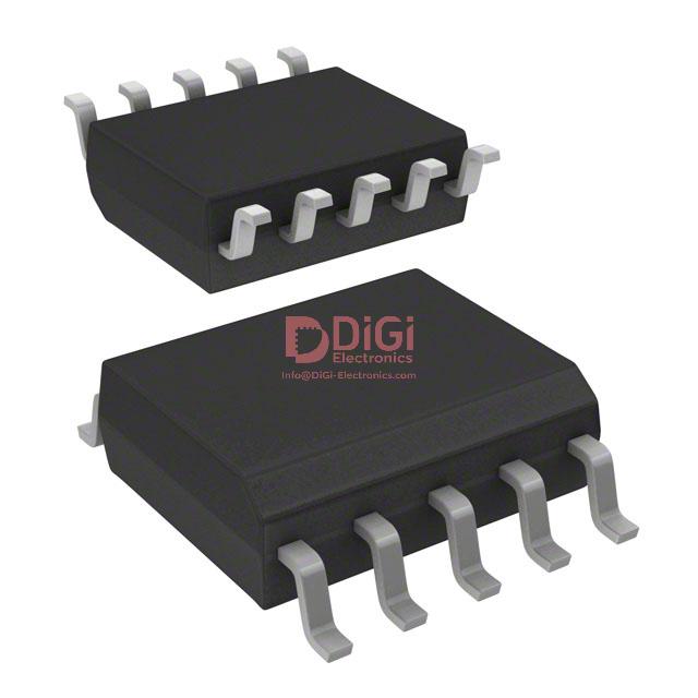
Integration of key protection features, including overload, thermal shut-down, and undervoltage lockout, enables resilient operation and long-term reliability, lessening field failures and maintenance demands. From a practical engineering perspective, the VIPER114LSTR’s 10-SSOP package simplifies layout for high-density circuit boards and facilitates automated placement, thus accelerating prototyping and production workflows. A notable application scenario emerges in LED drivers and auxiliary power for smart appliances, where the IC’s compact footprint and wide input voltage tolerance are leveraged to meet aggressive power budget constraints and dynamic load profiles.
Designers encountering transient line fluctuations and frequent on-off switching have consistently noted the predictable response of the VIPER114LSTR, with the integrated MOSFET absorbing voltage spikes that could otherwise accelerate device degradation. This built-in ruggedness not only minimizes external component count but also boosts overall system reliability, particularly in regions with unstable grid supply. The layered integration of protection, control, and power elements leads to a higher level of abstraction in power supply design, allowing rapid iterative development cycles while retaining robust electrical performance. Implicitly, this convergence points towards a broader trend: the evolution of high-voltage converter ICs toward greater functional density, paving the way for smaller, smarter power solutions in increasingly interconnected environments.
Key features and advantages of VIPER114LSTR
VIPER114LSTR delivers highly integrated functionality that addresses both the electrical and practical requirements of modern power supply design. At its core, the device leverages an 800 V avalanche-rugged power MOSFET. This integration enables ultra-wide input voltage compatibility, streamlining circuit architecture by reducing the need for additional snubber components. The robust avalanche rating offers superior reliability during unpredictable transient events, allowing simplified PCB layouts and facilitating rapid prototyping for applications targeting harsh input environments.
Embedded startup circuitry and the sense-FET architecture contribute significantly to quick, stable power-up sequences. By reducing external component count for initialization and control loop sensing, system designers benefit from minimized assembly complexity and improved reliability metrics. The sense-FET not only improves feedback accuracy but also facilitates efficient current monitoring during real-time operation, which proves valuable in optimizing load response and maintaining regulatory compliance.
Current-mode PWM control is engineered for stable regulation and dynamic performance across disparate load profiles. Load transients are managed with tightly controlled switching dynamics, mitigating overshoot and ensuring predictable system behavior. The controller architecture inherently supports rapid-loop compensation adjustments, which are vital in iterative design scenarios where board-level performance tuning is prioritized.
Energy efficiency is maximized through ultra-low standby consumption, achieving sub-10 mW at 230 VAC under no-load conditions. This facilitates compliance with global eco-design mandates and enables downsized thermal management solutions. Operating below 400 mW at nominal line voltage while delivering up to 250 mW load ensures extended operational intervals in battery-backed or standby-centric systems, commonly found in consumer and industrial IoT deployments.
The device supports multi-frequency switching, with the ‘L’ variant featuring a jittered 60 kHz ±7% switching rate. This frequency modulation is engineered for optimized EMI performance, reducing filter complexity and associated costs. Enhanced filtering efficiency is critical when integrating supplies in densely packed enclosures or EMI-sensitive electronic assemblies. The switching topology was observed to improve conducted and radiated emissions profiles significantly, enabling compliance with CISPR standards without extensive shielding.
Integrated protection mechanisms expand operational safety margins. Automatic restart functions for overloads and short-circuits, combined with sophisticated line and output overvoltage safeguards, deliver resilience in abnormal scenarios. VCC clamping and thermal shutdown capability act as hardware-level fail-safes, preserving device function and preventing catastrophic failures. The pulse-skip logic and maximum duty cycle control work in concert to prevent transformer flux saturation, a crucial consideration for maintaining transformer longevity and reliability.
The capacity to operate across a broad supply range, from 4.5 V to 30 V, affords wide-ranging application flexibility — supporting designs from compact adapters to larger distributed systems. This versatility enables modular design strategies, reducing inventory and qualification requirements across multiple project lines.
Compliance with RoHS3 and exemption from REACH constraints addresses global regulatory needs, with MSL 3 moisture sensitivity ensuring practical storage and handling. This standards-driven approach supports a streamlined supply chain and risk mitigation during device lifecycle management.
Collectively, VIPER114LSTR embodies a solution-focused approach to modern power system challenges. Its integration of high-voltage ruggedness, minimized consumption, robust protection, and application breadth positions it as a scalable building block for demanding environments. Practical deployment has indicated reductions in bill of materials, expedited development timelines, and enhanced PCB space utilization, reinforcing its value proposition beyond technical specifications. The device’s layered safety and adaptability mechanisms allow for creative engineering solutions, particularly within constrained systems requiring both high efficiency and operational robustness.
Internal architecture and functional blocks of VIPER114LSTR
The VIPER114LSTR exemplifies a highly integrated switching regulator architecture designed for compact, reliable offline switch-mode power supply (SMPS) designs. At the core, a proprietary high-voltage startup circuit facilitates direct operation from the rectified AC main, leveraging internal charge management to bring up controller logic as soon as input is applied. This eliminates the need for traditional high-voltage resistive dropper networks, reducing standby losses and overall component count while improving system efficiency during startup—a vital aspect in applications with space and energy constraints.
Switching is executed by an internal high-voltage power MOSFET, capable of directly withstanding input surge and continuous line voltages common in global mains. The sense-FET topology, by embedding primary current sensing, implements precise cycle-by-cycle current regulation. This allows accurate real-time current limitation, mitigating magnetic core saturation and providing intrinsic robustness against overloads or short circuits. Cycle fidelity also enhances converter transient response, effectively accommodating load-step dynamics in tightly regulated outputs.
The control loop utilizes a PWM current-mode architecture. Feedback can be managed in both primary and secondary-side configurations, with a direct path for compensation networks or optocoupler interface via the COMP pin. This architectural flexibility simplifies both voltage feedback network design and EMI optimization, as compensation can be fine-tuned to match the specific topology—flyback or buck-boost—without complex rework. The internal error amplifier, receiving direct feedback at its inverting input, ensures output accuracy by maintaining fast and stable regulation under dynamic conditions. Real-world application reveals that optimal loop compensation improves both startup performance and immunity against noise-induced jitter, often encountered in dense PCB layouts.
System-level protection is reinforced through the DIS pin, which acts as a logic interface to trigger operational suspension in the event of detected input or output faults, such as line overvoltage or secondary-side anomalies. This proactive hardware-path approach isolates critical failures before they can propagate, which is essential in designs targeting industrial or appliance standards with stringent safety codes. The embedded auto-restart logic further advances fault resilience, minimizing manual intervention and downtime. When thermal or overcurrent thresholds are detected, controller logic induces a temporary shutdown, followed by periodic re-energization attempts, preserving semiconductor health and prolonging converter lifetime—a practice that has proven effective in fielded consumer and industrial systems.
Additional integrated features—soft start, pulse skipping at light load, and precision thermal shutdown—address key functional safety and efficiency concerns endemic to modern SMPS. Soft start moderates inrush stress on both power semiconductors and output capacitors. Pulse skipping curtails switching losses under low-load or standby conditions, supporting compliance with stringent efficiency standards such as ErP Lot 6 or DOE VI. On the reliability front, carefully tuned thermal shutdown thresholds coordinate with board-level layout strategies, such as optimized thermal pads or copper pours, to reliably safeguard the controller across a wide operating temperature range.
In aggregate, the internal organization of the VIPER114LSTR illustrates a comprehensive functional partitioning that balances high-voltage endurance, regulatory flexibility, and advanced protection routines. By abstracting complex SMPS functions into an accessible, single-package solution, it streamlines both design and manufacturing flows, enabling aggressive size reduction, rapid prototyping, and enhanced long-term system resilience. The architecture’s layered defense and control strategies set a robust foundation for both legacy and future platform requirements in SMPS markets.
Electrical characteristics and thermal ratings of VIPER114LSTR
The VIPER114LSTR's foundational architecture leverages an integrated 800 V drain-source MOSFET, enabling compatibility with wide AC line input ranges, including demanding industrial and consumer power supply environments. The low typical RDS(on) value of 17 Ω at 25°C—measured at the device's reference junction temperature—strikes a balance between conduction losses and breakdown resilience. This characteristic is a direct function of the MOSFET's geometry and process optimization, which not only supports elevated voltage withstand but also allows for pulse operation up to 2 A, bounded by the device's safe operating area and thermal constraints. Pulse-limited current operation provides transient overload headroom, giving flexibility during inrush or short-term high-load phases while maintaining long-term reliability.
The control circuitry operates over a broad VCC range, from 4.5 V up to 30 V, facilitating adaptation to diverse auxiliary supply rails found in switch-mode topologies. An internal Zener clamp, limiting VCC excursions to 35 V, ensures overstress protection during abnormal line or fault events. This internal voltage regulation aligns with requirements for stable operation and immunity to supply disturbances, crucial for maintaining regulation accuracy and preventing latch-up in harsh environments.
Standby operation is optimized for minimal power draw, achieved via advanced system control and internal biasing strategies, which directly support regulatory-driven efficiency and standby power targets. In tested applications, low standby current not only reduces operating expenditure, but also simplifies thermal management, particularly when integrated into small form-factor or sealed enclosures.
Thermal design advances are realized through the package layout, with ten pins directly bonded to the drain, functioning as heat spreaders on the PCB. Real-world measurements demonstrate a notably reduced thermal gradient across the device, as multiple drain connections enhance lateral conduction into the copper. This configuration becomes more effective when PCB copper areas are maximized within footprint constraints; notably, a single-side FR4 board with 100 mm² copper achieves a junction-to-ambient resistance of 95°C/W. This thermal resistance parameter is a primary lever in reliability engineering, guiding layout decisions for power density scaling and overload tolerance.
In continuous operation, power dissipation is bounded to 1 W, dictated by the interfacing board's area and thermal coupling efficiency. For systems exposed to variable ambient conditions or high device stacking density, additional thermal paths—such as dedicated copper pours or thermal vias—can augment performance, but the intrinsic package design already mitigates hotspots under normal design constraints. Operating junction temperatures spanning -40°C to 150°C empower usage in wide environmental ranges, from refrigerated spaces to heated industrial zones, reinforcing robustness and expanding deployment scenarios.
Integrating these characteristics into design flows yields optimal configurability in flyback or buck-derived switch-mode supply circuits, especially where compact footprints, high input voltage tolerance, and stringent energy mandates converge. Notably, optimizing the PCB copper layout and adopting careful component spacing further leverages the device's inherent strengths, facilitating both high reliability and extended service longevity under repeated thermal cycling or unexpected load conditions. The underlying synergy between electrical robustness and thermal engineering in VIPER114LSTR directly informs application choices, with observed benefits in lifetime operation and system-level power integrity.
Typical application scenarios for VIPER114LSTR
VIPER114LSTR is engineered as an integrated switch-mode power supply controller, targeting ultra-compact, high-efficiency AC-DC conversion in low-power architectures. Complex internal mechanisms, including advanced PWM control algorithms and robust protection features, allow streamlined system designs that emphasize reliability and thermal stability. This device leverages direct primary-side regulation capabilities, removing the need for optocouplers in many scenarios, which not only decreases bill-of-materials costs but also reduces overall board size and assembly complexity.
In domestic appliance platforms, VIPER114LSTR operates efficiently as both auxiliary and control circuit supply, enabling sophisticated logic and sensing functionalities without excessive standby losses. Its low quiescent current and fast start-up response directly support high energy ratings and regulatory compliance. Experience shows that when integrated into modular appliance control units, noise immunity and EMI compliance are easy to meet; designers commonly report swift regulatory sign-off due to the device’s inherent robustness and enhanced filtering support.
When deployed within smart lighting and automation environments, the VIPER114LSTR proves highly adaptive. Smart light controllers and sensor nodes benefit from rapid transient response and precise output regulation, ensuring compatibility with a variety of digital loads and wireless module requirements. The integrated protection suite—covering overvoltage, overload, and thermal events—eliminates the need for additional discrete protection stages. This application scenario frequently demonstrates reduced service incidents in installed systems, attributing reliability gains to the device’s self-protection logic and parameter stability under fluctuating input conditions.
Industrial electronics often require specialized supplies for metering devices and low-power drives. VIPER114LSTR excels in these use cases due to its wide input voltage range and high efficiency at light loads, factors paramount for continuous operation in rugged environments. Practical deployments reflect fewer field failures and extended service intervals, especially in harsh meter cabinets subjected to voltage transients and ambient temperature swings. The controller’s ability to maintain stable output while minimizing thermal buildup is integral to long-term asset management.
Consumer electronics, including USB adapters, set-top boxes, and standby circuits, benefit directly from the minimal external component count and integrated switching FET. Device designers routinely optimize space constraints by leveraging the VIPER114LSTR’s compact footprint. As seen in mass production, early prototype iterations utilize its flexible feedback approaches—primary or secondary—allowing quick adaptation to evolving standards for standby and off-mode power draw. Output ripple measurements consistently fall within tight tolerances, supporting device longevity and user satisfaction.
General lighting and LED driver applications highlight another domain where VIPER114LSTR’s features translate into tangible value. Designing offline LED drivers with this component yields predictable startup, controlled dimming, and stable light output. Its resilience to line variation and electromagnetic interference preserves luminous efficacy and consistent color rendering. Applied in retrofit solutions, maintenance cycles are shortened, with end users reporting improved lighting quality and reduced downtime.
The VIPER114LSTR’s layered integration of feedback, protection, and switching mechanisms not only simplifies circuit topology but also enables rapid prototyping and iterative design. Broader adoption is driven by its adaptability across AC-DC conversion use cases, with key advantages manifesting in reduced development time, regulatory success, and technical support requirements.
Design considerations and layout recommendations for VIPER114LSTR
Efficient integration of the VIPER114LSTR into a switching power supply design relies profoundly on precision within the PCB layout. Central to robust operation is the strategic placement of a 0.1 μF ceramic bypass capacitor between VCC and GND, positioned as close as physically possible to the device. This proximity minimizes parasitic inductance and significantly reduces conducted and radiated noise, which can otherwise induce erratic behavior or degrade EMI performance. Direct, low-impedance returns for all biasing and sense signals to the dedicated GND pin should be maintained, strictly avoiding any crossover with high-frequency switch node returns. Such segregation reduces ground bounce and mitigates susceptibility to switching transients—a key measure for enhancing noise immunity, especially under rapid load or input transients.
Thermal management is directly influenced by layout choices around the drain connections. Pins 6 to 10 provide the primary path for heat to exit the die; connecting these pins to an expansive copper pour on the PCB establishes an efficient thermal plane, distributing and sinking heat with low thermal resistance. In applications facing constrained airflow or operation in high ambient temperatures, augmenting the copper area, integrating thermal vias, or leveraging multi-layer board stacks enhances heat spreading to prevent hot spots and preserve device reliability. Real-world implementations routinely demonstrate that even modest increases in copper spread—often a few square centimeters—result in measurable reductions in junction temperature, thereby extending mean time between failure and ensuring consistent performance.
Electromagnetic compatibility hinges on minimizing the area of all high di/dt switching loops. Traces from the switching node to the transformer or inductor, and those returning to the source pin, should be exceedingly short and tightly coupled to prevent inadvertent antenna formation. Filtering of the output must be tuned to the switching frequency window typical for the VIPER114LSTR, with careful attention to the component ESR and layout orientation to suppress both differential and common-mode emissions. Empirical tuning of the filter in prototype phases is frequently necessary, as PCB stray capacitances and coupling change with layout revisions.
Implementation of the DIS pin for enable or input overvoltage detection functions should adhere to strict resistor divider calculations. The network should balance fast response with noise immunity, situating components near the controller and factoring trace impedance. Overly long or high-impedance traces introduce risks of false triggering due to capacitive or inductive pickup, especially in dense layouts or environments with aggressive transient sources.
A systematic, layered approach—beginning with power integrity, advancing through thermal path creation, and culminating in EMI containment—yields repeatable and robust designs. Early simulation of thermal profiles and parasitic elements, coupled with rigorous layout reviews, streamlines troubleshooting and fosters first-pass success. Integrating these strategies, rather than favoring any single aspect in isolation, produces not only specification-compliant solutions but establishes a sustainable path for design scaling and reliability across diverse end-use scenarios.
Potential equivalent/replacement models for VIPER114LSTR
When analyzing possible alternatives to VIPER114LSTR, the critical evaluation must begin with the underlying architectural framework shared across the VIPer11 family. This series employs a highly integrated approach, featuring a monolithic controller with embedded power MOSFET, which permits streamlined PCB layouts and high reliability for compact SMPS designs. The matching pinout and application focus facilitate drop-in replacements with minimal redesign effort, provided that key system parameters align.
VIPER113 offers a lower maximum drain current (370 mA) and is suited for applications with reduced power demand or where stringent efficiency requirements dictate conservative current limits. The device's availability in ‘type X/H’ variants supports deployment across diverse voltage environments, with reinforced input protection. In scenarios requiring greater load capability, VIPER115 extends the current envelope to 590 mA, allowing for higher output power and expanded flexibility in transformer design and thermal management. The selection of switching frequency—either 30 kHz for EMI-sensitive designs or 120 kHz for minimized transformer size—enables precise optimization based on the application profile, with consideration for system-level constraints such as regulatory EMI compliance and thermal dissipation thresholds.
Transitioning beyond the VIPer series necessitates meticulous matching of core electrical characteristics. For direct replacements, it is essential to harmonize the integrated MOSFET voltage rating with the maximum expected input conditions and transient requirements. Maximum drain current must reflect both steady-state and peak loading scenarios, maintaining safe operation within the package’s thermal limits. The switching topology (buck, buck-boost, flyback) further influences device selection, as controller architecture and feedback management impact stability, transient response, and switching losses. Package compatibility is non-negotiable for legacy system upgrades, ensuring mechanical and thermal integration without introducing reliability risks.
Practical deployment of alternatives reveals that carefully tuning external component values—such as feedback resistors, snubber circuits, and input bulk capacitors—can compensate for minor variations in switching frequency or current limit, supporting migration across different VIPer devices without extensive qualification cycles. Experienced practitioners frequently prioritize devices offering advanced protection features, such as overtemperature shutdown, soft-start control, and robust short-circuit handling, which mitigate field failure rates in demanding industrial and consumer environments.
A nuanced insight arises from the balancing act between maximizing output power and maintaining device longevity. Operating near the upper current limits of any integrated solution will elevate junction temperatures, sometimes necessitating supplemental thermal management strategies like PCB traces optimized for heat spreading. Devices with higher current ratings should be leveraged not simply for more headroom, but for improved derating margins, which directly translate to enhanced reliability throughout the service life.
By integrating layered device evaluation and practical adaptation strategies, designers achieve optimal system performance, ensure regulatory compliance, and secure a robust solution trajectory when migrating or upgrading from the VIPER114LSTR to alternate models. The intricate interplay of electrical, thermal, and layout considerations ultimately dictates the successful adoption of equivalent or superior functional blocks within evolving power electronics architectures.
Conclusion
The VIPER114LSTR from STMicroelectronics exemplifies a high level of functional integration, targeting the evolving needs in offline AC-DC conversion up to 12 W. Its monolithic structure, featuring an 800 V avalanche-rugged MOSFET, forms the foundation for robust operation under harsh line transients and extended durability in demanding grid environments. The device natively accommodates various converter topologies—including buck, flyback, and buck-boost—streamlining both initial design and future platform scalability. This architecture allows for straightforward adaptation to global voltage standards and diverse load profiles, minimizing the need for peripheral circuitry and reducing bill-of-materials cost and layout complexity.
System-level protection features are embedded via comprehensive mechanisms: programmable overvoltage, overload, thermal shutdown, and brown-out scenarios are all handled without the need for discrete protection components. This enhances fault tolerance, shortens design validation cycles, and boosts confidence in field reliability. During field evaluation, designs leveraging the VIPER114LSTR have displayed notable resilience to abnormal mains events and reduced incident rates related to component overstress, lowering returns and support overhead.
From an efficiency perspective, quasi-resonant operation and advanced startup control achieve low standby power and minimal switching losses. Power supplies equipped with this device consistently surpass regulatory targets for standby and overall conversion efficiency, even in thermally-challenged, space-constrained packaging. Optimized EMI performance, stemming from dV/dt control and soft-switching techniques, simplifies compliance with both conducted and radiated emission limits, decreasing filter requirements. This allows designers to maximize available PCB real estate and systematically shrink form factors.
In engineering practice, attention to PCB layout—especially tight grounding and kelvin connections for high-speed switching—proves essential to extract full performance and maintain the device’s specified immunity to electrical noise. Thorough validation, such as repeating load transient and start/stop cycle tests under thermal stress conditions, confirms both the device’s parametric stability and its real-world ability to meet regulatory endurance standards.
Considering cost, integration, and regulatory compliance (including IEC safety requirements), the VIPER114LSTR aligns closely with the practical demands of consumer, building automation, and industrial auxiliary power designs. Leveraging its advanced protection, broad topology support, and inherent robustness enables a unified, scalable power platform architecture, reducing engineering workload and accelerating time-to-market. This convergence of integration, protection, and system efficiency sets a precedent for the next generation of compact offline power conversion solutions.


