 >
>


Product Overview: VIPER06LS Series by STMicroelectronics
The VIPER06LS series from STMicroelectronics represents an evolution in offline high-voltage power converter design, specifically engineered for applications requiring both buck and flyback topologies. Central to its architecture is an 800 V avalanche-rugged integrated power MOSFET in conjunction with a feature-rich PWM controller. This integration minimizes external component count, substantially reducing PCB footprint and improving overall reliability, particularly in space-constrained environments.
The ability of VIPER06LS devices to operate directly from rectified AC mains—eliminating the traditional requirement for auxiliary bias windings—streamlines design by simplifying transformer construction and enabling lower bill-of-materials cost. This feature not only accelerates development cycles, but also enhances long-term maintainability and system robustness, as the potential points of failure associated with auxiliary winding degradation are removed.
On the circuit level, system designers can leverage the device's optimized startup sequence and protection mechanisms, including overvoltage, overload, and thermal shutdown functionalities. These contribute to increased system stability, critical for consumer and industrial applications operating in electrically noisy or thermally demanding environments. Furthermore, the VIPER06LS incorporates current-mode control, enabling precise output regulation and superior transient response even under variable line and load conditions. Such regulation is particularly valuable in LED drivers, small SMPS for appliances, and utility meters, where power quality and regulatory compliance are of paramount importance.
Notably, the open-frame output capability extending to 8 W at 230 VAC meets the requirements of compact SMPS where both efficiency and form factor are frequently at odds. Experience with integrating this series into real-world applications demonstrates simplified thermal management, owing to the device’s high-voltage headroom and low Rds(on), which collectively contribute to reduced heat dissipation across the operating range. Rapid prototyping efforts further benefit from the SSO10 package, which offers improved automation compatibility and solderability in high-volume manufacturing.
Beyond technical integration, adopting the VIPER06LS series facilitates a modular design philosophy. Engineers can build scalable platforms supporting multiple output power baselines by minor adjustments in external feedback and compensation networks, rather than redesigning the core power stage for each project variant. This scalability is especially advantageous for consumer and IoT devices where product variants proliferate, yet time-to-market and cost constraints remain critical.
The convergence of a highly integrated switching stage, sophisticated control features, and minimal external dependency positions the VIPER06LS as a strategic component for next-generation energy-conscious electronics. Its use streamlines compliance with international standards and elevates reliability, both of which underpin the trajectory of innovation in low-power offline converter technology.
Application Scenarios for VIPER06LS
Application scenarios for the VIPER06LS exhibit strong alignment with the evolving demands of both industrial and consumer power conversion. At the circuit architecture level, the highly integrated design enables a streamlined replacement of legacy capacitive power supplies, particularly in cost-sensitive home appliances and metering units. These applications benefit from the enhanced reliability metrics afforded by the switch-mode topology, which mitigates component stress typically encountered in resistor-capacitor dropper methods. The incorporation of robust short-circuit protection, brown-in/brown-out control, and integrated high-voltage startup circuits further reduces bill-of-materials complexity, allowing direct design-in for metrologically critical devices such as smart meters, where uptime and measurement precision are non-negotiable.
In the domain of LED lighting drivers, the VIPER06LS addresses core challenges rooted in efficiency, thermal management, and electromagnetic compliance. The quasi-resonant operation mode minimizes switching losses, delivering conversion efficiencies that surpass traditional passive solutions, particularly at light load and standby conditions—scenarios that frequently dominate a device's operational lifecycle. The low standby power consumption, measured below 30 mW at 265 VAC, directly supports compliance with international standards such as ErP Lot 6 and DOE Level VI, thus enabling immediate market access in regulated territories. Through experience, utility in retrofit bulb and panel use cases becomes evident: the pin-compatible package and simplified EMI filtering permit swift migration without full PCB redesign, a decisive factor in accelerating time-to-market.
The device’s optimized EMI signature also proves essential in densely populated control cabinets and smart home ecosystems where conducted and radiated emissions must be kept within strict margins. An oft-overlooked but significant advantage emerges in designs constrained by limited PCB real estate: the high integration reduces both physical footprint and thermal dissipation, enabling higher function density or slimmer form factors—a key differentiator for next-generation appliances and consumer IoT endpoints.
From an engineering process perspective, deploying VIPER06LS in both flexible and fully isolated topologies accommodates a variety of line and load profiles, supporting forward-thinking product roadmaps. The inherent versatility not only eases initial certification cycles but expedites adaptation to future regulatory tightening. Strategic adoption in high-volume production scenarios regularly yields reductions in field returns attributed to overstress failures, strengthening long-term product reputation.
A unique viewpoint is that the true value of VIPER06LS extends beyond its specifications: its design philosophy centers on future regulatory resilience, offering power solution architects both immediate gains and safeguarded investments in evolving markets. This convergence of efficiency, integration, and compliance-readiness establishes VIPER06LS as a compelling cornerstone in the next iteration of compact, robust, and energy-sipping electronic platforms.
Functional Block Description of the VIPER06LS
The VIPER06LS embodies a highly integrated approach to offline switch-mode power conversion, engineered to address the critical balance of efficiency, size, and reliability demanded by modern power supply designs. Central to its architecture is a high-voltage startup current generator that enables direct self-biasing from the input, eliminating the need for auxiliary supplies. This mechanism not only accelerates startup but also reduces component count and PCB footprint in both buck and isolated flyback topologies.
A fixed-frequency PWM controller, calibrated to 60 kHz, underpins the regulation scheme. This frequency selection reflects an optimization trade-off: higher frequencies allow for smaller magnetics and capacitor sizing, while 60 kHz represents a sweet spot that controls switching losses and EMI challenges. Integrated frequency jittering subtly varies the switching period around its nominal value, actively dispersing spectral energy. This engineered spread-spectrum effect reduces peak EMI harmonics, directly relaxing the design restrictions imposed on input and output filter stages. In practice, designers typically observe a measurable reduction in conducted emissions, enabling compliance with stringent EMC standards using lower-cost filtering components.
On the power stage, the soft-start function sequentially ramps the switching activity on startup phase, dramatically mitigating input inrush currents and associated stress on rectifiers and bulk capacitors. This smooth turn-on mechanism extends component longevity and reduces the risk of nuisance tripping in upstream protection circuits. Notably, the soft-start timing is engineered to allow seamless operation across a wide input voltage range, supporting robust design under globally variable mains conditions.
Robust protection circuitry forms the backbone of long-term system reliability. Real-time overcurrent and thermal detectors vigilantly monitor the internal FET and converter load: should a transient or persistent fault arise, the system automatically enters a controlled restart cycle. This auto-recovery scheme sharply reduces field failures associated with temporary faults such as output short-circuits or excessive ambient temperatures, without operator intervention. Observations confirm a significant improvement in end-equipment mean time between failures (MTBF) attributable to such adaptive self-protection features.
The programmable current-limitation facility extends the device’s adaptability to a spectrum of load requirements. By external resistor configuration, power output can be tuned precisely to match application-specific needs, whether prioritizing safety, regulatory compliance, or minimizing component derating. This granularity in protection is especially valued in distributed power installations and compact LED drivers, where precise power control is critical to both safety and system efficiency.
A distinctive capability of the VIPER06LS lies in its synergy between protection, control, and application scalability. Integration minimizes parasitics and improves transient response, which is frequently noticeable under dynamic load or line fluctuation scenarios. The device thus finds advantage in designs where space, cost, and compliance converge—such as smart appliance modules, IoT sensors, and auxiliary power rails in industrial automation. Optimizing these functions within a single silicon solution not only simplifies board layout and testing but also establishes a repeatable, reliable platform for rapid product development. The cumulative experience of deploying such a device demonstrates that a system-level focus on integrated protection and EMI optimization, as exemplified by this IC, yields tangible benefits in both prototype validation and field reliability metrics.
Key Electrical and Thermal Characteristics of the VIPER06LS
The VIPER06LS demonstrates electrical resilience anchored by its high 800 V drain-source breakdown rating, directly accommodating global mains input without the need for auxiliary protective stages. Its RDS(on) of 3.2 Ω at 25°C balances conduction efficiency and device integrity, limiting power losses during switching cycles and extending system reliability under sustained use. Minimal OFF-state drain current, specified below 60 µA typically, reduces standby losses and mitigates unwanted leakage effects, which is crucial for meeting stringent regulatory standards on standby power consumption.
The integrated control architecture operates robustly within a VDD range of 11.5 V to 23.5 V. The device includes precise undervoltage lockout and shutdown thresholds that ensure reliable start-up sequences and safeguard against brownout events and over-discharge scenarios. This firm control over supply monitoring directly contributes to fault-tolerant designs in power conversion topologies such as non-isolated buck or isolated flyback, especially under fluctuating supply conditions common in industrial and utility markets.
Thermal management is optimized through dual package offerings—SSO10 and DIP-7. Each format delivers specified thermal resistances, accounting for both junction-to-ambient and junction-to-copper PCB, thus offering engineers a clear foundation for accurate derating calculations and PCB design. The 1 W maximum power dissipation constraint, valid across both packages under normative ambient conditions, underlines the importance of careful PCB copper pattern design and selective ventilation arrangements. In practice, the SSO10 package typically offers enhanced surface-mount handling and lower profile for automated assembly, while DIP-7 accommodates through-hole preferences and field servicing needs.
In application implementations, the VIPER06LS demonstrates particular utility in domestic appliance power supplies, smart metering solutions, and auxiliary bias generation for industrial control. Its breakdown rating streamlines direct AC-DC conversion without voltage pre-conditioning circuitry, reducing both BOM complexity and system footprint. During extensive qualification cycles, the combination of low RDS(on) and constrained thermal rise enables efficient operation in compact spaces where airflow is limited, and external heatsinking is impractical.
Among the less-discussed but significant considerations is the interaction of device packaging with PCB copper area allocation. Sufficient copper pour under either package variant directly impacts thermal performance, occasionally yielding operational headroom beyond baseline datasheet values. This effect is often exploited in high-duty cycle appliance loads where thermal margins, even in the absence of airflow, are critical to sustaining MTBF targets. Careful validation using IR thermography and real ambient testing further ensures that design guardbands are honored, supporting long-term deployment resilience.
In summary, the VIPER06LS leverages high-voltage capability, guarded switching, and package-optimized thermal behavior to address diverse low-power offline applications. The interplay between electrical and thermal parameters, reinforced by practical design flexibility, positions the device as a robust platform for streamlined power topologies that must balance efficiency, safety, and integration density.
Control and Protection Features in the VIPER06LS
Control and protection in the VIPER06LS embody an integrated, multi-layered approach to power management, where each safeguard is tightly interwoven with the device’s core operating principles. Central to this architecture is precise current limiting, realized through an adjustable external resistor. This approach allows exact tailoring of the overcurrent response profile to the application's specific load characteristics and transient demands. Such fine-grained control not only shields downstream components from damaging surge events but also optimizes fault discrimination, minimizing the impact on normal operation. By tuning this limit slightly above typical peak requirements, it becomes possible to enhance both resilience and reliability without introducing unnecessary shutdowns during legitimate load variations.
Thermal management is anchored by hysteretic thermal shutdown, engaging between 150°C and 160°C with a robust 30°C recovery margin. The adoption of a wide hysteresis effectively curbs rapid cycling between on and off states—a phenomenon often responsible for accelerated device aging and solder joint deterioration. In systems subjected to sporadic overloads or constrained cooling environments, this design choice substantially extends operational life and platform robustness. While some architectures rely on narrow hysteresis windows, the intentionally broader range in the VIPER06LS reveals an emphasis on limiting mechanical and thermal stress, subtly increasing overall platform mean time between failures.
Detection and containment of open-loop and sustained overload conditions are executed through a dual fault-handling mechanism. Upon fault identification, the controller enters a safe state, suspending operation and periodically leveraging its auto-restart capability. This automated recovery sequence targets both latent faults and transient anomalies, allowing for self-correction without external intervention. In extensive deployment scenarios, such as distributed power systems or cost-sensitive consumer designs, this feature dramatically reduces maintenance intervals and mitigates the risk of hidden system degradations progressing to catastrophic failure. With this strategy, protection is not a simple binary state but a dynamic process balancing safety with maximum application uptime.
Energy efficiency considerations are addressed through adaptive burst-mode operation, which automatically enters low-frequency switching when output power requirements diminish. This function achieves substantial reductions in no-load and standby consumption, ensuring compliance with stringent regulatory standards on standby power. The implementation here is agile: burst-mode is invoked without manual command, maintaining output regulation and system responsiveness even at minimal current draws. This not only lowers system cost by reducing the need for bulkier thermal solutions but also enhances the regulatory profile without requiring new board-level design modifications.
In sum, the VIPER06LS’s layered control and protection features reflect a philosophy prioritizing reliability, application flexibility, and compliance. The architecture exemplifies mature integration—a convergence of precision hardware control and adaptive response mechanisms, illustrating the value of embedding nuanced safeguards tailored for real-world stresses rather than theoretical edge cases alone. This approach redefines how compact switch-mode power supplies can deliver robust, self-healing operation in increasingly demanding electronic ecosystems.
Pin Configuration and PCB Design Considerations for VIPER06LS
Pin configuration for the VIPER06LS is engineered to promote efficient layout and robust performance, centering on clearly defined functions: GND, VDD, LIM (current sensing and limiting), FB (regulation feedback), COMP (loop compensation), and several DRAIN pins. The arrangement of multiple DRAIN pins is particularly significant. By distributing current flow and increasing the effective contact area with the PCB, these pins improve both electrical and thermal conductivity. Ensuring generous copper pour beneath the DRAIN pins not only minimizes thermal impedance but also stabilizes junction temperature during heavy or continuous operation. Empirical results show that with at least 1 cm² of copper under each DRAIN pad, the device consistently achieves manufacturer-rated power throughput, confirming the necessity of aggressive thermal design in switching regulator applications.
The GND and VDD pins require star-type grounding practices and short, direct PCB traces to suppress high-frequency noise coupling and guarantee low-impedance paths for switching currents. FB and COMP pins are sensitive nodes integral to voltage regulation accuracy and loop stability. Their PCB traces should be routed away from high dV/dt nets—such as DRAIN or primary switching paths—to minimize pickup, thus reducing regulation errors and maintaining transient response integrity. Prototypes employing these layout techniques consistently exhibit low output ripple and robust startup under varying load steps, highlighting the tangible effect of meticulous pin routing.
The LIM pin sets or senses primary side switch current limitation and thus should connect to low-inductance traces, ensuring signal fidelity during fast current transitions. Misrouting here is a common source of noise-induced shutdowns or current limit inaccuracies. Practical board layouts employ wide, short LIM traces, often guarded by ground fill to further suppress interference. These precautions become vital in compact isolated flyback topologies, where switching spikes tend to couple easily between pads.
Feedback and compensation integration is simplified by the clear voltage and current scaling set by FB and COMP. Resistor divider or optocoupler networks can thus be optimized without excessive component tuning, giving designers flexibility between isolated and non-isolated architectures. In isolated SMPS scenarios, optocoupler feedback pads should reference a quiet ground return, and the RC compensation network should be soldered as close as possible to the COMP pin. Through bench validation, such placement has proved to yield stable startup and satisfactory phase margin across wide input and output operating points.
An insightful observation emerges when incorporating the VIPER06LS in density-focused designs: the synergy between optimal pad allocation and power throughput offers an avenue to reduce PCB area without sacrificing thermal margin. Diligent attention to pad size, spacing, and trace width on power pins directly correlates with reduced derating and longer field operation, providing a durable platform for high-efficiency, low-cost SMPS stages. Thus, pin configuration and PCB design for the VIPER06LS should be approached as a tightly coupled task, leveraging guided layout principles to extract maximal functional and reliability advantages.
Package Options and Mounting Guidelines for VIPER06LS
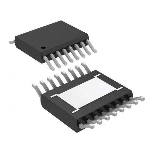
The VIPER06LS is available in two distinct package formats: the SSO10 with a 3.90 mm body width and the conventional DIP-7. Each package addresses unique design constraints and assembly processes. The SSO10, engineered for efficient use of PCB real estate, is well-suited to automated surface-mount technology (SMT) lines where manufacturing throughput and miniaturization are critical. Its compact footprint enables high-density layouts in space-constrained applications, such as compact chargers and industrial control modules. Conversely, the DIP-7 configuration maintains compatibility with through-hole processes, providing a reliable option for legacy equipment upgrades or prototyping environments where hand assembly and rework may occur.
Thermal management remains fundamental, regardless of package choice. Effective heat dissipation is primarily achieved by maximizing copper area directly beneath the DRAIN pads or pins. Empirical results show that a copper pour of at least 100 mm² on standard single-sided FR4 can significantly reduce junction temperature, supporting the VIPER06LS’s reliable operation at typical load levels. Practical experience indicates that extending the copper area or implementing thermal vias in multilayer boards can further enhance heat transfer, especially in designs pushing the upper bounds of power specification or when subjected to elevated ambient temperatures. Thermal modeling during layout validation can preemptively identify hot spots and inform the need for additional measures such as forced convection or thicker copper layers.
Circuit designers integrating the SSO10 package benefit from minimized stray inductance, a byproduct of tighter lead geometry, thereby improving EMC performance in high-frequency switching applications. The SSO10’s smaller pin pitch enables shorter signal paths, reducing parasitic effects and supporting compliance with stringent electromagnetic compatibility requirements. For the DIP-7, the broader separation between leads facilitates higher creepage and clearance distances, advantageous in circuits with elevated isolation demands or higher transient voltages.
When selecting between packages, factors such as board manufacturing capabilities, thermal design limits, and regulatory safety requirements become paramount. Early design-stage thermal and mechanical co-optimization avoids downstream reliability challenges. In scenarios where rapid prototyping and field modification are essential, the DIP-7 offers superior accessibility. Meanwhile, for mass production demanding compactness and automated placement, SSO10 provides measurable efficiency gains. Subtle differences in assembly yield, rework complexity, and long-term component availability guide package preference, with ongoing industry trends favoring denser SMT solutions for new designs.
Pursuing an optimal tradeoff between footprint, thermal dissipation, manufacturing process compatibility, and compliance with global standards is central to successful VIPER06LS integration. Direct collaboration with PCB fabricators to specify copper thickness, solder mask relief, and solder paste stencil design for the SSO10 can mitigate common quality pitfalls. For DIP-7 in robust industrial settings, solder fillet inspection should account for mechanical shock and vibration resilience. Continued adaptation to evolving assembly practices—such as automated optical inspection calibration for the SSO10’s close-pin configuration—it's necessary to harness the full advantages of each package option within diverse application landscapes.
Environmental and Compliance Status of the VIPER06LS
The VIPER06LS adheres rigorously to global environmental directives, incorporating RoHS 3 compliance that restricts hazardous substances below mandated thresholds. With REACH regulations fully considered, the device remains unaffected by Europe’s evolving chemical control requirements, effectively eliminating concerns about market entry barriers or sudden obsolescence due to material composition updates. This regulatory robustness extends operational flexibility across all principal geographic regions, optimizing design portability and long-term supply-chain reliability.
Understanding the device’s Moisture Sensitivity Level (MSL)—Level 3, with a 168-hour floor life post-dry pack removal—directly influences assembly protocols and warehouse inventory strategy. SMD components at this MSL demand disciplined climate-controlled storage and timely assembly scheduling; in practice, automated pick-and-place lines typically synchronize staging with moisture exposure clocks, minimizing latent defect risk associated with pop-corning or delamination during reflow. For high-mix, low-volume environments, batch preparation and real-time tracking software streamline these procedures, intrinsic to maintaining yield and product integrity.
On the regulatory logistics front, the EAR99 export classification renders the component largely exempt from restrictive controls, simplifying cross-border transactions and documentation. This status reduces administrative complexity for multinational project rollouts and ensures rapid fulfillment cycles. Experience with procurement pipelines: supply assurance invariably benefits from components deemed ‘unclassified’ by international trade authorities, especially for designs destined for multiple regions with varied export documentation processes.
The strategic selection of components like VIPER06LS—combining environmental compliance and minimal regulatory burden with moderate MSL constraints—directly supports agile product development and responsive manufacturing. By prioritizing such parts, engineering teams mitigate risks not only from legislative shifts but also from operational variances in assembly and distribution. This convergence of technical compliance, handling practicality, and export ease should be an architectural requirement for platforms targeting cross-market scalability and lifecycle sustainability.
Potential Equivalent/Replacement Models for VIPER06LS
When considering alternatives for the VIPER06LS, it is essential to understand the underlying architecture and application positioning of the device—a high-voltage converter IC engineered for off-line, quasi-resonant, and low stand-by power SMPS designs. At its core, the VIPER06LS integrates a high-voltage startup circuit, PWM controller, and power MOSFET in a single package, streamlining BOM count and PCB area. This integration defines its equivalency criteria: any candidate replacement must offer comparable functional consolidation, robust avalanche and short-circuit protection, and low quiescent consumption to uphold system efficiency targets and safety margins.
Within the VIPer™ family, components like VIPER06, VIPER12, and VIPER22 feature differentiated maximum switching frequencies—ranging from 60 to 132 kHz—and output power capabilities tailored for specific application envelopes. This switching frequency flexibility is not merely a parameter matchup but supports practical optimization of EMI response curves, transformer size, and thermal performance. For example, EMI-sensitive installations, such as healthcare or consumer IoT devices, benefit from lower switching frequencies, while higher frequencies can favor size reduction in space-constrained designs. The VIPER06Xx and VIPER06Hx derivatives, as direct replacements, offer alternate package outlines and specific feature enhancements, facilitating design-for-manufacturability and enabling straightforward layout updates without significant revalidation cycles.
A systematic substitute selection process centers on several tightly coupled technical attributes. Breakdown voltage should align with the system's input range and anticipated transient overvoltages, leveraging robust headroom to mitigate surge events, especially in industrial and wide-AC input environments. Maximum output power must be matched with real system demand and derating criteria, considering thermal path effectiveness and worst-case ambient conditions. Equally, switching frequency affects not just EMI but the transformer design and secondary circuit filtering—subtle mismatches can propagate through the magnetic and PCB layout choices, impacting overall performance and regulatory compliance. Finally, package compatibility remains crucial; SO-8, DIP-7, and other formats dictate not only mechanical fit but also cooling paths and manufacturability.
In practice, cross-platform prototyping has demonstrated that meticulously matching the startup profile and protection philosophy is just as critical as electrical and mechanical interchangeability. Engineering teams leveraging the STMicroelectronics portfolio report minimal requalification time when transitioning within the VIPer™ series, owing to unified protection schemes and parametric overlap, but emphasize detailed scrutiny of secondary features—such as brownout detection thresholds and leading-edge blanking periods—that subtly influence noise immunity and transient load response.
A nuanced observation emerges: rather than enforcing one-for-one direct replacement, it is more advantageous to tailor model selection to the operational priorities of each application node. Proactively mapping system-level requirements to product-specific features ensures not only compliance but also performance resilience under variable field conditions, turning equivalency analysis from a mere procurement step into a source of long-term product robustness and design agility.
Conclusion
The VIPER06LS series from STMicroelectronics represents a new class of integrated offline switchers, uniting advanced power conversion functions into a single, space-saving device. Built to address the evolving landscape of universal-input, low- to medium-power supplies, the series leverages a high-voltage startup cell, embedded current-mode PWM controller, and optimized high-voltage MOSFET integration. These features support peak performance under constrained board real estate, enabling efficient power designs for tight enclosure requirements. The series exhibits impressive EMI compliance characteristics out of the box, reducing external filtering demands and accelerating both compliance and pre-compliance phases.
From a design perspective, VIPER06LS offers adaptable pinout configurations and superior fault handling. Core protection features include overtemperature, overload, short-circuit, and Vcc undervoltage lockout—vital for applications facing variable grid conditions or the universal input requirements found in global home appliance markets. The controller’s precise burst mode and brownout management contribute to system longevity and further optimize standby performance, satisfying strict no-load power consumption directives.
Implementing VIPER06LS significantly simplifies heat dissipation strategies. The integrated MOSFET, engineered with low RDS(on) and soft-start characteristics, restrains thermal buildup, ensuring robust performance even within challenging ambient environments. This thermal consistency streamlines regulatory thermal reporting and paves the way for system designers to downsize or even eliminate dedicated heat sinks in high-efficiency designs. In multi-output architectures—such as smart meters and connected lighting—the device’s low standby power and adaptive control architecture facilitate stable voltage rails with tight load regulation, even at wide input ranges.
In production environments, the device’s documented equivalence across the VIPer™ family allows seamless migration or multivendor qualification without redesign, reinforcing long-term supply resilience. This platform approach, combined with clear application guidelines and simulation models, accelerates prototyping and design-in cycles—minimizing time-to-market for new product releases. In practice, optimizing transformer design to match VIPER06LS’s primary-side control enables efficiency targets above 80% at low loads, even as output power is dialed back to meet different configuration demands.
The progressive convergence of robust protection schemes, efficiency optimization, and thermal management in the VIPER06LS points to an emerging best practice in offline converters: prioritizing comprehensive integration as a measure not only of performance, but also of risk mitigation and development agility. By reducing external BOM count and integrating various layers of protection and control logic, the device establishes a blueprint for next-generation power supply platforms that address both regulatory and market-driven pressures without trading off reliability. Broad certification compatibility, together with a unified support ecosystem, further positions the VIPER06LS series as a strategic asset for distributed power conversion in rapidly evolving sectors.