>
>


Product overview: Sharp PC3Q510NIP0F optoisolator series
The Sharp PC3Q510NIP0F optoisolator series exemplifies a high-density approach to galvanic isolation, engineered explicitly for multi-channel environments that demand consistent separation and signal integrity. Its configuration integrates four channels within a space-efficient 16-pin mini-flat half-pitch SOIC package, optimizing both board real estate and functional granularity. This multilayer isolation architecture mitigates crosstalk, supporting applications that require parallel signal processing—such as precision programmable logic controllers, remote telemetry units, or advanced communication backplanes.
Central to each channel is the pairing of an infrared emitting diode and a Darlington phototransistor, a mechanism that blends high sensitivity with amplification. The Darlington configuration amplifies weak input signals while minimizing the need for substantial forward current to achieve reliable activation. This not only enables interface compatibility with low-power logic outputs but also broadens applicability to microcontroller-driven subsystems operating under tight energy budgets. By achieving strong current transfer ratios at minimal input levels, the device supports robust signal reception—particularly critical in systems subject to high electrical noise or variable loading.
A rated isolation voltage of 2500Vrms establishes a physical and electrical divide between primary and secondary circuits, a specification that resonates with requirements in industrial control panels, telecom distribution frames, and automation switching nodes. This degree of isolation fortifies long-term reliability against transients, surges, and ground potential differences, thus securing sensitive control logic from hazardous interference. In real-world circuit deployments, such separation reduces fault propagation, simplifying design certification for standards like IEC 61010 and reinforcing EMC resilience.
From assembly to field integration, practical challenges often arise in high-channel-density designs. The PC3Q510NIP0F package allows for simplified routing, reducing parasitics and unwanted capacitive coupling compared to discrete solutions. Through judicious placement and optimized leadframe geometry, engineers can control signal skew and maintain consistent propagation delays across all channels. In power delivery or signal transcoding applications, such uniformity underscores operational stability—especially in synchronized multi-axis drives or real-time sensor arrays.
One key insight is the strategic deployment of the Darlington output stage, which inherently benefits systems confronting wide input dynamic ranges or non-standard signaling protocols. Leveraging this design, circuit architects can tailor interface thresholds and biasing without excessive external circuitry, thereby minimizing complexity and cost. The optoisolator’s four-channel integration additionally supports modular expansion, simplifying system scalability in equipment racks and distributed I/O modules.
Layering signal isolation, amplification, and miniaturization within a single device, the PC3Q510NIP0F series demonstrates how thoughtful optoelectronic design catalyzes efficiency and system reliability in modern control infrastructures. This approach not only solves electrical isolation challenges but also streamlines engineering workflows, from initial prototyping to large-scale production deployment.
Key features of the Sharp PC3Q510NIP0F series
The PC3Q510NIP0F series is engineered to streamline optoelectronic signal isolation in compact electronic assemblies, with critical features addressing both manufacturing and operational constraints. At the mechanical level, the adoption of double transfer mold construction enhances physical integrity and thermal resistance, directly supporting high-reliability soldering processes such as flow soldering. This robust encapsulation mitigates moisture ingress and minimizes the risk of void-related failures, a notable concern during mass production. The optimized form factor, specifically its four-channel integration and 1.27mm lead pitch, supports efficient routing in dense PCBs, while the low package mass aids in reducing mechanical stress when subjected to vibration or thermal cycling.
From an electrical perspective, the series employs a Darlington phototransistor output topology, achieving a current transfer ratio (CTR) of at least 600% at an input current of only 0.5mA. This architecture significantly improves input-to-output amplification, ensuring reliable logic level translation even with minimal driving current. The low input current aligns with low-power control circuits, such as microcontroller GPIOs, which often operate under constrained supply budgets. In practice, this permits direct interface without auxiliary buffer stages, reducing total component count and potential sources of signal delay.
Electrical safety and compliance considerations are meticulously addressed by the device’s lead-free and RoHS-conformant bill of materials. This guarantees suitability for applications across regulated markets, removing concerns related to hazardous substance restrictions. The standardized lead spacing further ensures compatibility with both automated and manual assembly workflows, mitigating issues often faced with unconventional footprints.
Application-wise, the PC3Q510NIP0F is particularly effective in microcontroller signal isolation in space-constrained environments, such as industrial control modules and instrumentation backplanes. Its reliability in high-density layouts translates to reduced cross-talk and increased noise immunity, contributing to stable system performance even in electrically noisy settings. The combination of high amplification, robust packaging, and compliance with international standards makes the series a preferred choice in scenarios where assembly yield, long-term reliability, and environmental assurance are paramount.
A core insight arises from the interplay between device efficiency and system-level integration: the ultra-low input drive requirement, paired with high CTR, unlocks new design possibilities in energy-sensitive ecosystems, particularly when upstream interface circuitry must maintain functionality over wide supply variations. This nuanced optimization of the input-output characteristic curve sets the series apart, linking foundational package engineering to superior real-world performance metrics.
Agency approvals and compliance for Sharp PC3Q510NIP0F
Agency approvals and compliance constitute critical considerations in the selection and deployment of the Sharp PC3Q510NIP0F optoisolator, particularly within the context of industrial and telecom environments governed by rigorous safety and reliability standards. The device is recognized under UL1577 for double protection isolation, validated by file No. E64380 and listed as model No. PC3Q51. This means the optoisolator is tested to withstand high isolation voltage, supporting system resilience against electrical surges and potential fault propagation across isolated sections. UL1577 recognition directly influences PCB layout strategies, allowing for reduction in design uncertainties related to insulation requirements. Incorporating devices with double protection also assists in satisfying both end-equipment and subsystem safety certifications, minimizing the need for supplementary isolation mechanisms.
In parallel, the use of a resin conforming to UL 94V-0 flammability grade addresses fire risk mitigation at the component level. This flammability rating confirms self-extinguishing characteristics under test conditions, aligning with industry best practices for limiting propagation of thermal events. Engineers leveraging components with UL 94V-0 rating can implement compliance strategies for system-level standards such as IEC 60950-1 and IEC 62368-1; these standards often trace safety down to material selection for critical parts. In rapidly evolving markets, using pre-certified optoisolators streamlines product acceptance processes and reduces time-to-market by satisfying baseline regulatory checklists without extensive pre-qualification testing.
Field deployment often reveals nuanced considerations not explicit in datasheets: for instance, leveraging agency-certified optoisolators in circuit designs promotes uniformity in factory audits and facilitates cross-border product launches, as major regulatory bodies defer to harmonized safety marks. Selection of the PC3Q510NIP0F, given its dual agency credentials, creates an engineering advantage by consolidating isolation and flame retardance within a singular, easily audited BOM entry—sidestepping the complications of assembling isolation from discrete uncertified elements.
Application scenarios such as programmable logic controllers (PLCs), signal isolation in base stations, or protection circuits for power line communication depend not merely on the electrical specifications of isolation components, but also on the verifiable, documented chain of compliance. By embodying both robust materials engineering and formal agency approval, the Sharp PC3Q510NIP0F not only simplifies the path to global conformance but also reduces the engineering overhead associated with risk and variance management in regulatory submissions. This layered integration of safety, reliability, and certification efficiency positions the component as an optimal choice for high-stakes environments where system integrity cannot be compromised.
Internal structure and connection details of Sharp PC3Q510NIP0F
The PC3Q510NIP0F integrates multiple optocoupler channels, each featuring a high-efficiency infrared emitting diode (IRED) precisely aligned with a Darlington phototransistor output stage. This device architecture leverages optical coupling, achieving robust signal isolation between the input and output sides. The IRED, positioned for minimal light path loss, transmits modulated infrared signals, which the phototransistor array detects and amplifies, yielding significant current transfer ratios essential for driving downstream digital or analog loads.
The pinout schema assigns clear roles: dedicated pins for the IRED’s anode and cathode directly connect to control or logic sources, while the phototransistor collector and emitter terminals simplify output stage design. Internal parasitic capacitance and layout symmetry in the device mitigate crosstalk among channels, enabling parallel integration within high-density circuit boards. This isolation ensures immunity against voltage transients and ground loops, a necessity for mixed-signal domains or systems susceptible to noise propagation.
Effective PCB implementation requires careful attention to trace impedance and separation on both input and output paths. Matching LED forward currents and configuring external pull-up or pull-down resistors at the output permit rapid switching with minimal propagation delay. Experience demonstrates that maintaining adequate spacing between channels and shielding critical nodes further suppresses electromagnetic interference—a common challenge in closely packed industrial control modules or switching power supplies.
Counter to one-size-fits-all approaches, optimal deployment of the PC3Q510NIP0F often involves tailoring drive circuitry to match specific output current and voltage requirements. Fine-tuning the series resistor values on the IRED side enables precise control of LED brightness and device response. In safety-critical or high-reliability contexts, redundant channel wiring and regular parametric verification ensure long-term device stability, leveraging the Darlington output’s inherent sensitivity for early fault detection.
Beyond textbook application, detailed understanding of the internal arrangement informs advanced diagnostic protocols, such as monitoring minute shifts in forward voltage or leakage currents to predict component aging. In sum, a systematic approach to both schematic-level planning and board-level execution unlocks the full performance and reliability potential of the PC3Q510NIP0F in demanding optoisolation scenarios.
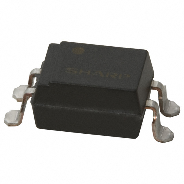
Pin configuration and package information of Sharp PC3Q510NIP0F
The Sharp PC3Q510NIP0F optoisolator integrates four isolated channels within a 16-pin mini-flat SOIC package, optimizing space constraints and facilitating clean signal routing in densely populated PCB layouts. Each channel’s pin configuration dedicates specific anode-cathode pairs for input, and emitter-collector pairs for output, enabling individual control and isolation of multiple signals. This structural arrangement ensures minimal channel crosstalk and precise timing integrity, particularly essential in applications demanding error-free, high-speed signal transmission between noisy power domains and sensitive logic circuits.
The physical construction leverages tin-copper (SnCu) lead plating, typically with 2% copper content, aligning robustness with RoHS compliance and supporting high-reliability, lead-free SMT assembly. The lead plating enhances wettability during reflow, reduces oxidation risks, and maintains solder joint integrity across thermal cycles, which is especially valuable in systems subjected to frequent temperature variation or mechanical stress.
Marking conventions for the PC3Q510NIP0F omit rank indicators, opting for a streamlined legend—an approach that simplifies lot tracking and inventory handling yet demands attention to the 20-year repeating date code cycle. Careful lifecycle documentation is suggested to mitigate identifiability issues when integrating in long-service products and to maintain traceability for field replacements.
From an implementation perspective, the discrete channel architecture provides flexibility when isolating interface boundaries, such as microcontroller I/O expansion in industrial automation or high-side monitoring in power supplies. Parallel channel design reduces layout complexity when routing control signals, improving EMC performance through reduced ground loops. The package’s mechanical footprint supports rapid prototyping and in-circuit debugging, enhancing development velocity in safety-critical designs.
The convergence of robust mechanical features, adaptable electrical isolation, and clear package standards positions the PC3Q510NIP0F as a compelling solution for both established and emerging multiplexed isolation tasks. Selection criteria should account for not only signal integrity and isolation voltage but also long-term product traceability, SMT process reliability, and system-level maintainability—a multidimensional evaluation that ensures sustained operation in advanced electronic assemblies.
Absolute maximum ratings and electro-optical characteristics of Sharp PC3Q510NIP0F
Adhering to absolute maximum ratings is critical for ensuring long-term reliability and operational integrity of the Sharp PC3Q510NIP0F optocoupler. Each rating—covering input current, output voltage, collector-emitter voltage, and isolation voltage—demarcates the threshold beyond which device degradation or catastrophic failure can occur, even under transient conditions. Maintaining all operating parameters, including pulse width and duty ratio, within these specified limits mitigates risks associated with thermal runaway and excessive junction stress.
Internally, device architecture relies on an infrared emitter-phototransistor pair, whose performance is strongly temperature dependent. Electro-optical characteristics, measured precisely at an ambient temperature of 25°C, provide a reliable baseline for transfer ratio, turn-on and turn-off times, and leakage currents. This characterization at nominal conditions allows for predictable circuit behavior, essential for tight tolerance designs in control and signal isolation applications. Performance shifts beyond 25°C, particularly above the specified humidity range or with increased input pulse energy, may induce changes in phototransistor response, impacting the linearity and timing of signal transmission. Therefore, derating strategies become vital for systems operating outside standard lab conditions.
In practice, strict control over environmental variables—such as maintaining proper airflow on densely populated boards and using conformal coatings for humidity protection—enables stable operation and extends device longevity. Engineers consistently monitor input drive levels and power dissipation, ensuring that current transfer ratio remains within calculated ranges across varying duty cycles. Precision in pulse shaping and careful selection of PCB materials further mitigates parasitic capacitance and thermal drift, crucial for high-frequency applications.
The balance between absolute maxima and practical operating ranges underpins robust system design. Integrating optocouplers like the PC3Q510NIP0F within feedback loops or as digital isolation nodes requires holistic consideration of both the published device characteristics and real-world variations. Recognizing that electro-optical parameters are not static prompts adoption of adaptive biasing and temperature compensation methods, securing signal fidelity across diverse environments. This layered approach translates into systems that not only avoid component-level failures but also deliver consistent functional margins over extended lifetimes.
Performance characteristics of Sharp PC3Q510NIP0F under varying conditions
The Sharp PC3Q510NIP0F optoisolator exhibits performance profiles that align with the core requirements of isolation, signal integrity, and reliability across a range of operating variables. Key parameters—forward current, ambient temperature, and power dissipation—interact to define operational envelopes that demand precise calibration in high-density control systems. As forward current increases, incremental thermal stress is observed, directly impacting the maximum allowable collector and total power dissipation. Effective thermal derating is integral to sustained function, particularly when ambient temperatures rise or board spacing is minimized. In practical deployment, reliance on datasheet limits without real-world system validation can result in premature degradation, emphasizing the need for conservative derating and active heat-dissipation strategies when device count is high.
Current transfer ratio (CTR) emerges as a pivotal metric, deeply influenced by input current magnitude and aging effects under continuous operation. At lower input currents, CTR variability increases, affecting small-signal responsiveness and precise threshold detection—an aspect critical in analog feedback systems or low-voltage logic interfacing. Empirical observation suggests that CTR stability can be enhanced by operating above minimum recommended drive currents, but this must be balanced against cumulative thermal load and long-term LED wear-out mechanisms. Under repeated thermal cycling, persistent monitoring of CTR drift becomes valuable, particularly when optocouplers are utilized in adaptive or fail-safe circuitry.
Collector current characteristics as a function of collector-emitter voltage delineate the saturation and active regions of the device, informing the optimal biasing strategy for both speed and efficiency. In application, low collector-emitter voltages can precipitate increased leakage and response time variability, especially when device arrays are subjected to simultaneous switching. Load resistance significantly affects response time; heavier loads extend switching delay, potentially introducing signal skew in tightly synchronized environments. Engineering practice recommends cross-verification of laboratory time-domain waveforms with end-system load profiles to preempt deterministic timing faults.
Graphical data from detailed product characterization, while foundational to the design phase, should be augmented by in-circuit measurement under representative environmental conditions. Addressing system-specific derating, real-time power cycling, and variance analysis delivers superior confidence in robust field performance. A nuanced understanding of these layered dependencies enables the architecting of optoisolated channels exhibiting both predictable behavior and logistical flexibility, an advantage particularly apparent in the design of modular or mission-critical automation platforms.
Proactive engineering thus leverages intrinsic device parameters in concert with pragmatic validation and risk management, transforming static specification compliance into dynamic system longevity and stability.
Design considerations for engineering with Sharp PC3Q510NIP0F
Engineering with the Sharp PC3Q510NIP0F demands an understanding of its optoelectronic behavior under real-world constraints. At the device level, current transfer ratio (CTR) stability forms a central pillar of predictable circuit performance. When operating below the minimum specified input current threshold of 0.5 mA, CTR dispersion widens, affecting signal integrity in sensitive interfaces. This necessitates conservative design margins in the input stage, especially in environments where supply fluctuation or tolerance stacking can momentarily drive the input below optimum levels.
LED emission degradation is intrinsic to the forward-biased IRED architecture. Over prolonged operation—typically beyond 40,000 hours—a 50% output decrease quantifies its aging trajectory. This degradation modifies downstream circuit response and influences optoisolator reliability planning in embedded systems. Designers integrate this characteristic into preventive maintenance schedules or select periodic recalibration cycles in precision automation. In compact modules, CTR compensation algorithms offset the effect, balancing device wear against system specification drift without frequent hardware service.
The optoelectronic suitability of the PC3Q510NIP0F hinges on understanding its non-coherent IRED source and its insensitivity to irradiation. These attributes make the component appropriate for controlled, non-extreme operating environments but exclude applications requiring radiation hardening, such as aerospace or nuclear systems. In field deployments, such limitations guide protective enclosure designs and environmental qualification.
Extensive reference to targeted application notes enables architectural optimization, unlocking advanced biasing topologies or signal conditioning techniques tailored to the device’s unique radiometric and electrical curve. In manufacturing or test scenarios, leveraging this documentation allows for tighter control of measurable parameters, reducing out-of-spec unit incidence.
Maintaining signal fidelity over deployment lifetimes calls for integration of component aging factors into the initial design calculus. Incorporating real-world experience, circuit designers achieve robust product lifecycle management by using statistical monitoring of CTR drift and preemptively selecting optoisolators with low initial CTR spread in high-reliability applications. This layered approach, coupled with appropriate environmental safeguarding, establishes the PC3Q510NIP0F as a consistent solution within its performance envelope, particularly in industrial controls, instrumentation, and modular automation platforms.
Manufacturing and assembly guidelines for Sharp PC3Q510NIP0F
Manufacturing and assembly procedures for the Sharp PC3Q510NIP0F necessitate strict adherence to temperature management and process cycles in all soldering operations to preserve optoelectronic performance and mechanical stability. Central to the device’s longevity is the enforcement of reflow soldering profiles that remain within specified thermal boundaries, as excessive thermal stress or repeated reflows can compromise the integrity of the plastic mold encapsulation and internal phototransistor junctions. Limiting reflow to no more than two solder cycles mitigates the cumulative risks of substrate delamination and pin lift, particularly relevant for units subjected to automated SMTA lines with variable dwell times.
The double transfer mold package enables compatibility with flow soldering, yet precise control is required. Exposure above 260°C for over ten seconds increases the likelihood of solder joint microcracks, especially at the lead-mold interface where differential expansion can induce stress concentration. Setting preheating intervals strictly between 100–150°C for 30–80 seconds not only optimizes flux activation but also buffers thermal gradients, which frequently cause pad peeling in high-density PCB designs. Empirical production runs have demonstrated that controlled ramp rates consistently yield better wetting behavior and reduce rework compared to aggressive thermal ramp-up protocols.
Hand soldering remains useful for repairs and low-volume assembly yet demands heightened process discipline. Completing operations within three seconds and maintaining an iron tip temperature below 400°C are pivotal measures to prevent localized overheating, which can degrade the optically transparent epoxy and the sensitive optical receiver elements. Experience shows that limiting solder cycles to two preserves bond pad adhesion and maintains electrical isolation, particularly in scenarios involving sequential component mounting where latent heat accumulation can occur.
Validation of each soldering regime under representative manufacturing conditions is critical to uncover latent failure mechanisms such as interfacial oxidation, void formation, or mechanical fatigue at the solder joints. Iterative process audits—supported by in-line AOI and cross-sectional microscopy—reveal that variance in board finish and footprint layouts can significantly influence interface reliability, especially in high-speed signal applications where minimal impedance discontinuity is required.
From a process engineering perspective, continuous monitoring of thermal profiles and attachment quality under actual throughput demands not only upholds device-level integrity but also streamlines yield rates and reduces root-cause analysis cycles for assembly defects. Leveraging these tightly defined guidelines as non-negotiable process constraints sets a robust foundation for sustainable reliability, particularly in applications demanding high optoelectronic signal fidelity and repeated thermal cycling.
Cleaning instructions and environmental compliance of Sharp PC3Q510NIP0F
Cleaning strategies for PCBs assembled with the Sharp PC3Q510NIP0F demand careful consideration of both component integrity and regulatory constraints. The device’s encapsulation tolerates solvent-based cleaning using ethyl, methyl, or isopropyl alcohol, provided process parameters remain tightly controlled—a maximum temperature of 45°C, and immersion limited to three minutes. Exceeding these limits can degrade optoisolator performance and compromise solder joint longevity. Prolonged exposure or elevated temperatures may induce stress cracks in the encapsulant or promote flux residue under the leadframe, necessitating post-clean inspection for residues via magnification or ionic contamination testing.
Ultrasonic cleaning offers an efficient alternative for flux removal, particularly where dense component populations restrict solvent flow. However, it requires calibrated assessment of bath characteristics: excessive ultrasonic power or inappropriate tank sizing can generate microcavitation-induced mechanical stress, risking leadframe detachment or polymer delamination. Suitability hinges on factors such as PCB thickness, mounting technology, and component pitch. Optimal results arise from pilot runs that replicate production circumstances, followed by electrical retest cycles to monitor device parameters such as CTR and isolation voltage.
In production environments prioritizing traceability and throughput, integrating solvent and ultrasonic methods in a staged process—gentle solvent pre-wash followed by low-power ultrasonic finishing—frequently yields superior ionic cleanliness without adverse physical impact. Continuous process monitoring, using meniscus tracking and real-time temperature logging, ensures that each cleaning step meets the device’s tolerance envelope.
The PC3Q510NIP0F’s design adheres strictly to RoHS (2002/95/EC) standards, verified free from hazardous elements including lead, mercury, cadmium, hexavalent chromium, PBB, and PBDEs. Additional exclusions include CFCs and Halons, addressing extended compliance with ozone-depleting substance regulations and broader industry environmental stewardship. This positions the device as an optimal solution for global deployment, eliminating concerns for restricted materials across regional markets.
Layering cleaning best practices with environmental compliance produces an integrated workflow—balancing rigorous contamination control with component safety and regulatory peace of mind. Field observations demonstrate increased device reliability and extended service life when cleaning protocols are standardized, technician training incorporates material constraints, and process validation includes environmental impact metrics. Ultimately, leveraging the RoHS compliance and robust cleaning compatibility of the PC3Q510NIP0F extends its utility in high-reliability, safety-critical systems, underscoring the importance of holistic maintenance strategies in contemporary electronics manufacturing.
Tape and reel packaging specifications for Sharp PC3Q510NIP0F
Tape and reel packaging for the Sharp PC3Q510NIP0F is engineered to optimize compatibility with automated assembly processes. Each optocoupler unit is loaded into PS (polystyrene) carrier tape, which ensures precise cavity dimensions and dimensional stability during transit and integration. The PS carrier tape provides robust protection against electrostatic discharge and mechanical stress, preventing device damage during handling and transportation. Encapsulation with a PET three-layer cover tape further stabilizes the components while providing a reliable peel force suited for high-speed pick-and-place feeders. This multi-layer cover tape avoids tape tears and ensures consistent cover removal across varying humidity and temperature ranges frequently encountered on assembly floors.
Each reel is designed to accommodate 1000 devices, a format that minimizes machine downtime for spool replacement and significantly reduces the risk of supply interruption during extended production runs. The configuration adheres to established EIA-481 standards, which define both pocket pitch and pitch tolerance, facilitating seamless integration into SMT lines with uniform reel winding and unspooling performance. Distinct orientation markings and insertion-direction arrows on both tape and reel eliminate placement errors at the feeder stage, directly supporting zero-defect manufacturing objectives.
In daily operation, the use of rigid PS carrier and PET cover tape demonstrates tangible improvements in throughput and device yield. When integrated with modern high-speed placement equipment, the uniformity of pocket alignment and cover tape consistency allow for aggressive feeder speeds without component misplacement or dropouts. Precise reel dimensioning—tight tolerance on hub diameter and outer flange—is vital; mismatches often cause tape tension irregularities, leading to feeder jams or splice errors. Experience shows that proper storage (humidity-controlled, upright reel stacking) further preserves tape integrity and component alignment, minimizing variation in pick rates as tapes approach the end of the reel.
From a reliability perspective, the choice of materials in the tape and cover system is non-trivial: PS carrier offers lower outgassing and minimal ionic residue compared to lower-grade plastics, reducing potential contamination risks in sensitive optoelectronic assemblies. PET cover tape's defined peel strength supports consistent adhesive performance over long storage times, maintaining reactivity for high-volume reflow environments.
When specifying or substituting packaging for the PC3Q510NIP0F, subtle differences in tape thickness, cover tape adhesion, and reel diameter have pronounced impacts on assembly yield and operational costs. Prioritizing materials and dimensions that match pick-and-place system tolerances is essential for achieving optimal results in high-throughput production. An iterative approach to tape validation and inventory rotation further enhances overall yield and process reliability. This systematic attention to detail at both material and process levels underpins robust, cost-effective automated assembly with the Sharp PC3Q510NIP0F.
Potential equivalent/replacement models for Sharp PC3Q510NIP0F
Potential replacement models for the Sharp PC3Q510NIP0F must precisely match its operational characteristics and interface requirements. This optoisolator features a four-pin DIP package, single-channel isolation, and a Darlington phototransistor output. System designers prioritizing footprint optimization and circuit simplicity often evaluate alternatives with identical response times, isolation voltages, and input sensitivity.
A close substitute, Sharp’s PC3H510NIP0F, achieves electrical equivalence while presenting a more compact form factor. It preserves the low input forward current typical of PC3Q510NIP0F, sustaining minimal drive power—critical for embedded and battery-powered circuits. The Darlington output configuration contributes both high current transfer ratio (CTR) and enhanced switching speed, enabling reliable interfacing with TTL and CMOS logic levels without additional amplification. Matching the pinout and voltage ratings enables direct drop-in replacement, reducing redesign efforts.
In practice, migration to a streamlined single-channel optoisolator simplifies PCB routing and component placement, especially in space-constrained signal isolation scenarios. For applications leveraging optocouplers in sensor interfacing or microcontroller inputs, reducing channel count minimizes parasitics and crosstalk. Field experience reveals that assembling PCBs with fewer optoelectronic variations improves manufacturing yield and traceability—beneficial in automated optical inspection workflows.
Selecting an equivalent model requires attention to package outline, CTR consistency at operating currents, and thermal derating curves under real-world loads. Testing with actual drive circuits occasionally reveals subtle variances in turn-off times or leakage, which diligent characterization with pulse generator setups can identify. Ensuring functional interchangeability involves not just datasheet comparison but empirical validation under representative loads and switching conditions.
A layered substitution approach—mapping both electrical and mechanical parameters—mitigates risk and preserves system integrity. Using form-compatible, performance-matched optocouplers like PC3H510NIP0F enables engineers to streamline layouts, maintain isolation ratings, and uphold stringent regulatory compliance, setting a practical foundation for scalable design evolution.
Conclusion
The Sharp PC3Q510NIP0F series optocouplers embody a combination of elevated isolation voltage ratings, minimized input drive currents, and stable current transfer ratio (CTR) behavior under varied operational environments. At the device level, the isolation barrier leverages advanced photosensitive coupling—typically a high-efficiency phototransistor separated from the LED source via proprietary encapsulation techniques. This structural approach not only maximizes isolation voltage, often exceeding 5kV (rms), but also ensures low parasitic capacitance, mitigating signal integrity issues across fast switching rates.
The efficient input current requirement enables seamless interface with microcontrollers, PLC outputs, and signal conditioning circuits, reducing component stress and power budget overhead. CTR uniformity is maintained through precision wafer-level processing and stringent quality assurance protocols, leading to predictable turn-on voltages and consistent output responses across manufacturing batches. Engineers routinely exploit these properties to architect galvanically isolated feedback loops in motor drives, inverter controls, and fieldbus transceivers. In such scenarios, reliability hinges on stable long-term operation under thermally and electrically stressful environments—attributes reinforced by the series’ tested compliance with EN/IEC insulation standards and RoHS environmental directives.
Integration flexibility is further enhanced by form factor options and lead pitch variations, facilitating drop-in assembly for surface mount or through-hole installations. Manufacturing partners benefit from simplified BOM management and reduced susceptibility to layout-caused crosstalk or spacing violations, especially when adhering to IPC-2221 recommendations for creepage and clearance. This minimizes post-assembly defect rates and fosters repeatable high-voltage isolation performance in modular system designs.
Within practical design cycles, the PC3Q510NIP0F series has demonstrated particular value in galvanic isolation blocks for multi-channel ADC systems. Low input current characteristics have allowed designers to parallel optocouplers with minimal board rework, while comprehensive regulatory documentation has accelerated qualification under UL and VDE standards. Attention to detail during layout—such as controlled ground referencing and thermal coupling to avoid temperature-induced CTR drift—has proven to enhance lifetime device consistency, especially in mission-critical installations such as medical or rail signaling hardware.
Emergent trends in signal isolation call for components that not only meet the baseline electrical and mechanical requirements but also enable system-level scalability. The inherent robustness and clear datasheet parameters of the PC3Q510NIP0F optocouplers position them as cornerstone devices for applications demanding rapid development, rigorous assurance, and design longevity. By leveraging their strong certification pedigree and integration efficiency, engineers gain a strategic component capable of supporting both legacy and next-generation equipment architectures.