


 >
>


Product Overview: MP2624GL-Z Charger IC
The MP2624GL-Z is an advanced, integrated switching-mode battery charger IC targeting single-cell lithium-ion and lithium-polymer applications. Its core architecture employs a synchronous step-down switching topology, optimizing both power efficiency and thermal performance under demanding load profiles. The device is packaged in a 22-pin QFN form factor with a compact 3 x 4 mm footprint, addressing the need for high-density PCB layouts where board real estate is at a premium.
At the circuit level, the MP2624GL-Z supports programmable charge current up to 4.5A. This high current capability stems from its robust internal switching FETs and precise current sensing architecture, which together minimize conduction and switching losses. Power path management is integrated, enabling seamless transition between adapter and battery power sources without service interruption. This feature is particularly valuable in handheld designs prioritizing zero system downtime and reliable hot-plug adapter handling.
A key differentiator is its USB OTG support, allowing the battery to back-power external peripherals via the USB port when required. This dual-role capability is critical in modern wearable, IoT, and mobile communication systems where the device may be required to act as both consumer and provider of energy. The programmable and protectable charging algorithms embedded in the MP2624GL-Z further mitigate thermal risk while maximizing charging throughput—essential for applications demanding rapid charge turnaround, such as POS terminals or ruggedized field instruments.
Fine-grained adjustment of charge parameters, exposed via configurable I/O and register access, enables optimization for specific battery chemistries, cell aging profiles, and thermal derating strategies. This enables design teams to precisely tune charging behavior for operational longevity and reduced field failure rates, addressing challenges in deployment environments with temperature extremes or varying power sourcing conditions.
In practical deployment, the high efficiency of the MP2624GL-Z, often exceeding 90% under nominal loads, mitigates thermal hotspots and reduces the need for extraneous heat sinking or airflow. This characteristic simplifies enclosure design and extends product lifetimes by limiting thermal cycling of PCB materials. Furthermore, its integrated safety features—overvoltage, overcurrent, thermal shutdown, and short-circuit protection—add a robust layer to system-level reliability, minimizing the external component count and potential failure points.
A subtle but noteworthy advantage is the device’s transient response and low quiescent current regime. These attributes ensure that sensitive analog circuits sharing the power rail are not adversely affected by supply noise during rapid load transients or in standby states, yielding more stable system operation in mixed-signal or RF applications.
The MP2624GL-Z demonstrates the convergence of compact design, configurability, and robust performance in the battery management domain. Its feature mix aligns tightly with the paradigm shift toward smaller, smarter, and more resilient portable electronics, where the ability to scale charging strategies and manage complex power domains is increasingly indispensable. Effective implementation of this IC in a project invariably results in streamlined PCB layouts, fewer design cycles adjusting heatsinking and protection circuitry, and expedited time-to-market for devices targeting performance-sensitive yet size- and efficiency-constrained sectors.
Applications and Engineering Context for MP2624GL-Z
The MP2624GL-Z integrates advanced charging management features tailored for mobile electronic platforms, addressing the increasing demands for efficiency and versatility in power systems. Central to its architecture is support for rapid battery charging through dynamic input current regulation, allowing seamless transition between various power sources—ranging from standard USB ports to higher-wattage wall adapters. This multi-input compatibility mitigates the constraints of legacy interface standards, ensuring optimal charging speed without risking device or battery integrity.
The device’s power-path management allows electronics to operate directly from input supplies, bypassing the battery during absence or deep discharge. This architectural design enables products to meet stringent uptime criteria, preventing system brownouts during battery replacement or initial shipment phases. As a result, MP2624GL-Z-based systems achieve improved resilience in field deployments, optimizing user experience and reducing support overhead.
From an engineering development lens, the solution simplifies PCB design by minimizing external component requirements, facilitating compact layouts in space-constrained form factors. Integrated safety, such as thermal regulation and fault protection, lessens the necessity for discrete monitoring circuitry and firmware intervention. This not only streamlines manufacturing, but also raises overall yield and system reliability.
In practical scenarios, rapid prototyping with MP2624GL-Z reveals predictable performance across wide input voltages and diverse battery chemistries. The configurable charging algorithms suit emerging high-capacity lithium batteries common in flagship devices. Subtle tuning of charge parameters—made possible by the device’s flexible interface—ensures thermal loads remain within design tolerances even under fast charging conditions, which is critical for safeguarding compact enclosures.
The innovation underlying MP2624GL-Z lies in the harmonization of charging speed and system protection, a convergence often challenging in portable device design. By integrating robust input management and system autonomy, it enables designers to navigate the trade-offs between miniaturization, charging flexibility, and platform reliability. This characteristic renders the device optimal for next-generation products where seamless operation and end-user trust align as primary development goals.
Key Features and Functional Block of the MP2624GL-Z
The MP2624GL-Z exemplifies integration by consolidating essential power management components into a single compact device, responding directly to the growing demands for highly efficient, reliable, and flexible battery-powered systems. At its electrical core, the reverse blocking MOSFET collaborates with stacked high-side and low-side FETs, orchestrating synchronous buck and boost conversion. This architecture not only isolates the system from unintended reverse currents but also enables rapid, loss-minimized transitions between charging and power delivery operations.
Driving both buck and boost topologies at a 1.5 MHz switching frequency, the MP2624GL-Z achieves a dramatic reduction in external passives. Components like inductors and capacitors shrink without sacrificing performance, facilitating significant board space savings and streamlined thermal management. Real-world validation reveals that carefully chosen layout techniques—such as direct gate routing and strategic copper pours—further curb electromagnetic interference and heat accumulation, fortifying reliability in dense multi-rail environments.
Voltage and current regulation precision—±0.5% for voltage and ±5% for current—stems from tightly coupled feedback loops and advanced error amplifiers. Such granularity directly translates into maximum cycle-to-cycle symmetry, ensuring battery longevity and stability over broad temperature and load ranges. Embedded current sense and control eliminate the need for external sensing elements, removing traditional points of failure and minimizing variability between production batches.
Thermal protection coverage extends to battery temperature monitoring, programmable safety timers, and comprehensive over-voltage safeguards, all governed by IEC 62368-1 AK requirements. Protection algorithms continuously adjust operational thresholds based on live data, making the device adept at handling dynamic charge profiles and transient events without manual intervention. System designers can capitalize on integrated metrics, reducing both firmware complexity and hardware redundancy.
The I²C programmable interface facilitates granular system control, with support for real-time parameter adjustment and event-driven diagnostics. Dual-mode selectors and custom firmware routines are easily implemented, allowing adaptive configuration for diverse battery chemistries and portable device constraints. Reliable field experience demonstrates that leveraging the I²C interface for closed-loop feedback sharply improves efficiency under fluctuating input sources.
Distinctively, designing with the MP2624GL-Z reveals a clear architectural separation between power conversion and system protection, yet it achieves seamless handshake through integrated logic. This modular focus heightens fault isolation, simplifies certification, and makes in-situ debugging more predictable. The synergy of robust hardware blocks with a flexible software edge marks a decisive improvement over legacy discrete solutions, especially in applications where multi-phase operation, scalable charge profiles, and tight form factor limitations coalesce—such as IoT nodes, industrial sensors, and consumer wearable devices.
Power Path Management and Battery Charging Architecture in MP2624GL-Z
Power path management within the MP2624GL-Z leverages a Narrow VDC (NVDC) topology to optimize both operational continuity and efficiency under diverse source and load conditions. At the foundational level, NVDC architecture orchestrates dynamic source prioritization—when input power is available, the system intelligently routes energy for immediate usage and battery charging. In scenarios where the battery is depleted or absent, the NVDC circuit ensures direct supply of the system by maintaining the VSYS rail above a programmable, reliable threshold. This design decision eliminates start-up latency and mitigates undervoltage stress, which is critical in mission-critical embedded applications.
The programmable minimum system voltage, accessible via the I²C interface, gives granular control over the operating threshold, allowing tight alignment with both the dynamic load profiles and battery chemistry requirements. Integrating a battery-side FET (field-effect transistor) provides an active decoupling function—this isolation enables maintenance, or even hot-swap scenarios, without risking system voltage collapse or transient-induced data loss. The approach improves not only reliability but also enhances safety, as fault conditions on one rail do not propagate unmitigated to the other.
Charging operations are finely staged to balance safety, longevity, and turnaround time. The initial trickle charge phase delivers a controlled 128mA into deeply discharged cells, activating recovery mechanisms while strictly limiting thermal stress and overcurrent risk to cell internals. Once a recoverable baseline voltage is reached, pre-charge mode initiates a measured current ramp, aligning charge acceptance with the battery’s safe operating envelope. Transition to constant-current fast-charge stage supports up to 4.5A (user programmable), which can be tuned via firmware for optimal trade-offs between speed and battery aging. This flexibility is often leveraged to harmonize high-capacity cell configurations with form factor constraints found in portable instrument design—real-world reliability hinges on careful ICC setting, minimizing both cycle time and heat buildup.
Terminal charging is governed by a constant-voltage phase, enforcing a well-characterized upper voltage limit for the cell type in use. This method inherently reduces current as full charge is approached, protecting against over-voltage and improving cycle life. The automatic recharge logic, operating as a voltage hysteresis function post full-charge, allows the system to maintain readiness without manual intervention. Following transient load or self-discharge, the device seamlessly re-engages charging, which is instrumental in deployment scenarios involving intermittent usage and prolonged standby.
A unique capability of the MP2624GL-Z lies in its battery supplement mode—a transparent energy-sharing mechanism that enables the battery to augment both system and input power sources. This dual feed architecture is critical when faced with input source droop, heavy pulsed loads, or mechanical disconnections at runtime. In practical deployment, supplement mode acts as a failsafe buffer, preventing sudden voltage collapse during load transients and thereby sustaining peripheral operation and data retention.
Core observations reveal that leveraging programmable NVDC control, granular charge phase management, and seamless supplement architecture collectively enhances design robustness, particularly in fields such as industrial data loggers, portable medical instruments, and high-reliability sensor nodes. Direct experience with dynamic load profile characterization underscores the practical necessity of flexible system voltage setting and proactive fault isolation—a design philosophy encapsulated in MP2624GL-Z’s architecture. Iterative firmware tuning, paired with real-world efficiency measurements, routinely demonstrates tight correlation between adaptive system voltage management and overall operational uptime, validating NVDC-centric strategies in advanced battery-powered system design.
USB Detection, Current Management, and OTG Operation with MP2624GL-Z
The integration of USB detection mechanisms in the MP2624GL-Z is rooted in compliance with the USB Battery Charging Specification 1.2 (BC1.2), as well as legacy USB2.0 and USB3.0 standards. The device executes protocol handshake sequences after plug-in events to identify the connected source, distinguishing between Dedicated Charging Ports (DCP), Charging Downstream Ports (CDP), and Standard Downstream Ports (SDP). This digital recognition translates directly into a precise mapping of allowable input currents, facilitating seamless compatibility with diverse USB infrastructures and maximizing charge rates without breaching host limitations.
Dynamic input current management is achieved by hardware logic and further configurable via the I²C interface, permitting on-the-fly adaptation aligned with source negotiation results. This closed-loop current programming is pivotal in applications where charging performance is often constrained by USB power host restrictions. With the tendency of consumer electronics to interface with various power sources, the adaptive input current setting eliminates undervoltage lockout and avoids input fuse tripping—a non-trivial challenge in robust USB-powered designs. The ability to fine-tune input levels in real time also aids in compliance with EMI thresholds and helps mitigate inrush current events during cable hot-plugging.
OTG support in the MP2624GL-Z extends the device’s utility by enabling reverse power delivery. In boost mode, a regulated 5V rail is sourced from the battery, with current capability scaling up to 1.3A. The architecture incorporates dual-layer control: hardware settings for fail-safe default operation, and I²C programmability for system-level policy enforcement. This flexibility is especially useful in embedded platforms where system firmware may dynamically enable or adjust peripheral power based on usage context, ensuring efficient load sharing and battery protection.
Safety is ensured by real-time monitoring and hardware-enforced limits for both short-circuit and over-voltage conditions on the OTG output. Rapid fault response is triggered without reliance on software interventions, delivering robust field-level protection against erratic peripherals, cable faults, or environmental stresses. Effective management of these risks is essential to guarantee device reliability in portable systems that must perform across variable and sometimes unpredictable connection scenarios.
System-level integration of the MP2624GL-Z, with layered detection and control mechanisms, addresses common pitfalls in USB charging and OTG deployment. The combination of adaptive current control, automatic source verification, and autonomous protection ensures optimal performance while safeguarding device integrity. In practice, tuning the I²C registers allows for fast iterative testing of power profiles during development, expediting qualification cycles and facilitating board-level validation against a variety of USB sources and OTG loads. This capability streamlines productization and enhances design agility when adapting to evolving USB power ecosystems.
The cohesive interplay of detection, current management, and OTG functionality in the MP2624GL-Z demonstrates a system-level approach to power path optimization, ensuring resilient and efficient performance across the increasing heterogeneity of USB connections. Such architectural choices reflect a broader trend toward intelligent, context-aware power management as a central pillar in next-generation embedded system design.
Charge Cycle Control and Safety Mechanisms in MP2624GL-Z
Charge cycle regulation in the MP2624GL-Z leverages multi-layered protection algorithms to secure battery integrity while optimizing charge efficiency. Immediate fault response mechanisms, such as integrated battery and system over-voltage detection, utilize precision comparators to halt charging or reroute system power, preempting electrical overstress and mitigating damage to adjacent circuitry. These responses are latency-minimized by integrating detection at the PMIC core, supporting rapid system recovery and fault isolation within mobile electronics design.
Thermal protection is managed through continuous monitoring via the negative temperature coefficient (NTC) thermistor interface. Charge currents are dynamically modulated based on thermal feedback, ensuring compliance with the JEITA charging profile. This dynamic adjustment is achieved through firmware-controlled DACs, balancing charge current and voltage in real time as thermal conditions shift. The result is maximized charging throughput without breaching manufacturer- or chemistry-specific thermal limits, particularly vital in form factor-constrained applications.
Programmable safety timers provide a second-tier defense against duration-related faults. Configurable via I²C or analog pins, these timers automatically suspend charge cycles that exceed expected durations, serving as a backstop for both hardware and firmware anomalies. This mechanism is particularly significant in the context of battery packs susceptible to capacity degradation or unpredictable aging characteristics, preventing overcharge in outlier scenarios.
Battery floating detection further enhances operational reliability by verifying battery installation status before any charge delivery. This process combines impedance measurement with low-current polling, reducing false positives from residual connectivity, and safeguarding against inadvertent charge application to absent, degraded, or incorrectly installed cells.
Power path efficiency results from low quiescent current during discharge—down to 20µA—and optimized FET architecture, featuring a 10mΩ on-resistance. This minimizes conduction loss, contributing to extended standby and active run times for mobile platforms. Practical deployment highlights that such low leakage is crucial in wearables and IoT edge devices, where maximizing uptime trumps all other metrics.
A layered interplay between hardware blocks and firmware control ensures high adaptability in diverse battery chemistries and system integration scenarios. Adaptive feature enabling—whereby only necessary protections are activated based on system telemetry—streamlines power consumption, simplified via register configuration. In deployment, this approach consistently yields lower fault rates over extended operational cycles.
Fundamentally, safeguarding battery health and user safety must remain tightly interwoven with system-level power management. The MP2624GL-Z demonstrates that high integration of real-time protection logic, configurable safeguards, and adaptive thermal throttling form the backbone of reliable charge cycle management, lending itself particularly well to compact, high-reliability consumer and industrial devices. Implicitly, coupling robust hardware design with flexible firmware hooks elevates fault tolerance and system longevity, a principle increasingly critical as battery technology continues to evolve and deployment environments diversify.
Programmability and I²C Interface of MP2624GL-Z
The MP2624GL-Z’s I²C interface forms the backbone for seamless configurability in battery management applications. At its foundation, the device implements a robust two-wire serial protocol, compliant with both standard and fast I²C speeds. This enables precise synchronization between the power management IC and external controllers, supporting communication rates up to 400 kbps for responsive system integration.
Programmability unfolds across multiple registers, each mapped to specific operational functions. Charging current, voltage thresholds, timer periods, input current limits, and thermal compensation coefficients are individually addressable, granting detailed, parameter-by-parameter configuration. System architects commonly leverage this granularity to tailor charging profiles to varying battery chemistries and use-case demands—such as fast-charging lithium-ion or temperature-sensitive nickel-metal hydride cells. Each setting is adjustable dynamically, allowing adaptive control depending on environmental conditions or system state. For example, tuning input current limits in real time enables coordinated power sharing when the device operates alongside other high-load subsystems.
The presence of immediate status and fault reporting mechanisms further distinguishes the interface. Information is continuously updated in dedicated registers, allowing rapid polling for voltage, current, fault flags, and charge completion indicators. Employing external interrupt triggers, connected hosts can respond to critical charger events—such as over-temperature, input over-voltage, or charge termination—with minimal latency. This real-time event notification is essential for designing fail-safe supervisory logic, reducing risk for battery damage or overheating without heavy resource overhead.
Operational modes are layered to maximize flexibility. Host-controlled mode allows full user oversight via software: every internal parameter can be actively adjusted to optimize performance for the current scenario. This mode is extensively used in device prototypes and production units where firmware updates drive functional enhancements over time. Default mode, conversely, ensures robust and safe power-up sequences, providing autonomous fallback operation if host connectivity is absent or compromised. Designers appreciate this duality in environments where fault tolerance and minimal intervention are prioritized.
A subtle but important experiential aspect involves balancing configuration complexity against runtime safety. The MP2624GL-Z’s register abstraction is intuitively designed, but practical implementation often involves rigorous validation—especially when transitioning settings dynamically during charge/discharge cycles. Lessons drawn from field deployments indicate enhanced reliability with staged parameter updates and explicit error handling routines, buffering transient faults and smoothing state transitions without sacrificing reactivity.
Integrating these mechanisms, one key perspective emerges: programmability encoded through a thoughtful I²C interface transcends mere convenience. It builds a foundation for agile, highly reliable battery charging, not only accommodating varied hardware requirements but actively enabling advanced power management strategies. This modularity empowers scaling from prototype experimentation to mass-market deployment, with real-time adaptability as a core benefit, directly facilitated by the IC’s layered communication structure.
Component Selection and PCB Design Guidelines for MP2624GL-Z
Optimal component selection and precise PCB design are vital for leveraging the full capabilities of the MP2624GL-Z, a high-efficiency power management IC. Each supporting element must be chosen and implemented with careful analysis, reflecting the interdependencies of electrical performance, thermal management, and system robustness.
Input current regulation is foundational for system integrity. The device offers configurability by either programming through I²C or applying a precision resistor to the ILIM pin. Calculating the input current limit utilizes the relationship IIN_LIMIT = 48.48 / R_ILIM[kΩ]. Selection of R_ILIM must balance desired current headroom with protection against unintended overload scenarios, while tolerances should be minimized to ensure consistent system behavior. Precision resistors within 1% or better are preferred to maintain predictable limits under varying temperature and aging.
Inductor specification drives the power stage’s transient behavior and efficiency. A 1.0µH inductor rated for saturation currents above 4.5A matches application profiles requiring high dynamic loads with compact converter design. However, increasing inductance to 2.2µH is beneficial in use-cases demanding lower voltage ripple and EMI suppression, such as precision analog front-ends or sensitive wireless modules. Elevated inductance translates to reduced ripple current, but mandates additional footprint and careful consideration of physical placement to avoid magnetic interference with adjacent circuits. Experienced designers often model ripple currents and assess peak versus RMS values during worst-case transients, validating selections against manufacturer saturation curves.
Capacitive selection at both input and output nodes directly impacts voltage stability and suppression of high-frequency noise. Employing low-ESR ceramic capacitors minimizes losses and resonates less with parasitic inductance, substantially dampening potential spikes. SYS node output capacitance at 22µF is a proven baseline for maintaining output voltage ripple under 0.5%, with tuning available through parallel additions if noise sensitivity warrants further mitigation. Placement must be directly adjacent to load and IC pins to avoid lead inductance, a recurrent source of overlooked oscillations in initial prototypes.
Temperature sensing integrates battery safety into the system through the NTC thermistor interface. The reference resistor divider, chosen to delineate the safe operating thermal window, requires matching the thermistor beta value and the specific cell thermal response. Calculations should anticipate manufacturing spread and drift, ensuring thresholds for charge/discharge cutoffs correspond with both the expected and worst-case peripheral conditions. Direct routing and minimal node parasitics increase response accuracy, as slow thermal reporting leads to risks of damage during over-temperature events.
PCB layout is paramount in translating schematic intent into functional hardware. High-current traces, especially those servicing the power path, demand minimal lengths and increased width to reduce IR drop and heating. Segregation of feedback and small-signal lines shields sensitive nodes from PWM switching noise—a frequent source of intermittent system anomalies. Thermal management is reinforced by extended ground and supply copper pours, which act as heat-spreading planes and lower overall impedance. High-density designs benefit from multi-layer stackups wherein power and ground layers are maximized in area, doubling as both current conduits and heat sinks. Critical communication lines such as I²C must follow independent and shielded routing, separated by ground or blank copper regions from pulsed current planes, thus securing data integrity against injected transients.
Iteratively testing layout decisions in representative operating scenarios rapidly uncovers latent weaknesses. For instance, switching-node proximity to analog sections can manifest as unpredictable noise bursts, resolved by re-layout or adding ground shields. Dimensional optimization, often employing electromagnetic simulation tools, enables recognizing coupling paths invisible in schematic capture. Integrating yield and process tolerance data into component selection ensures resilience to production variations, reducing field failures and post-deployment support loads.
Practical application demonstrates that reliability and performance hinge less on theoretical maximums and more on consistent engineering judgment—balancing specification targets, physical realities, and manufacturability. The synthesis of tight design discipline with empirical validation forms the backbone of robust MP2624GL-Z system integration, markedly reducing time to production readiness and field anomalies.
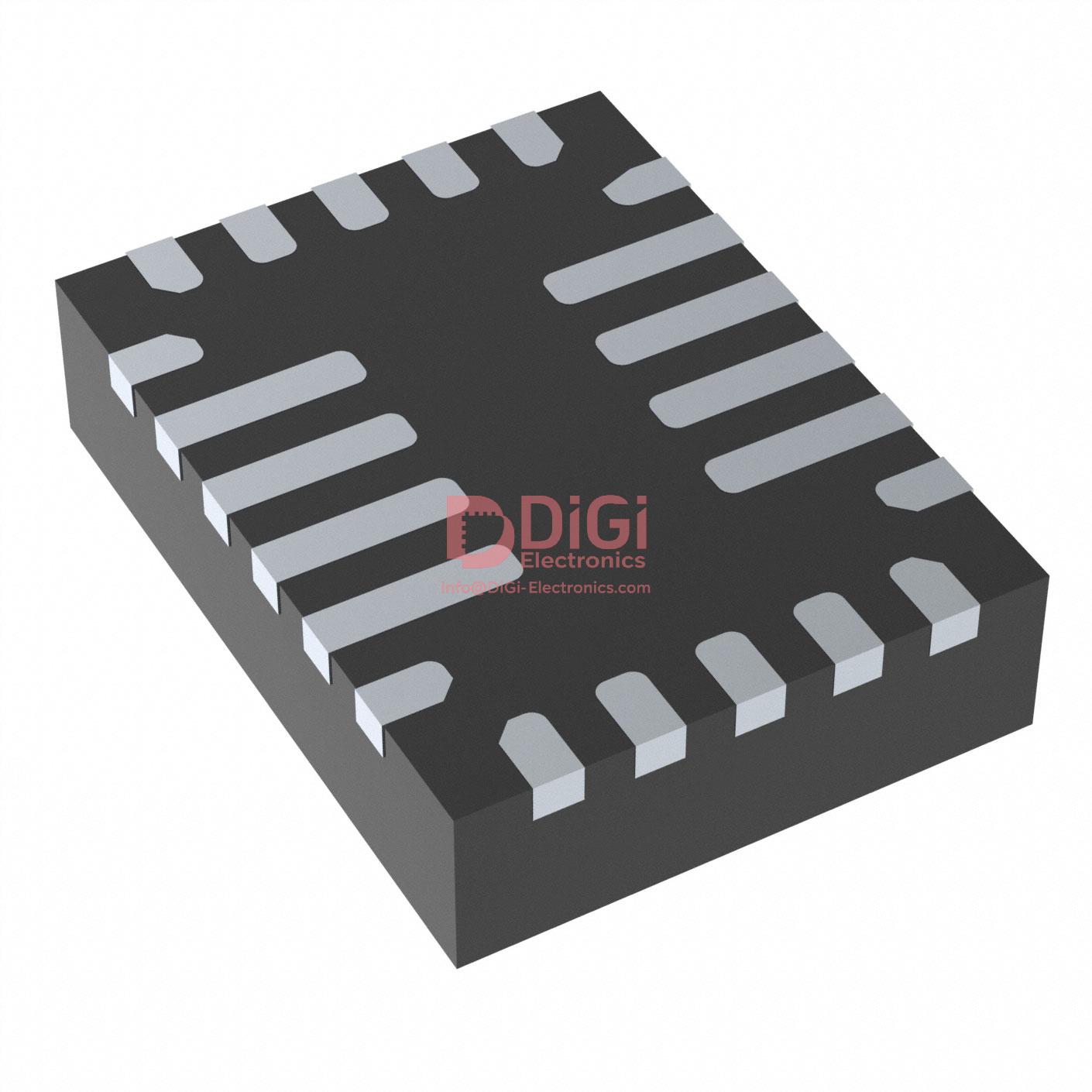
Package Information for MP2624GL-Z (QFN-22)
The MP2624GL-Z leverages the compact QFN-22 (3mm × 4mm) packaging, adhering to JEDEC MQ220 specifications to enable high-density PCB designs. This package architecture strategically addresses the challenges of thermal dissipation and spatial constraints in contemporary handheld and portable systems. The footprint supports dense component placement, optimizing board real estate without sacrificing thermal integrity or electrical performance.
At the core, the QFN-22 configuration achieves thermal efficiency through an exposed thermal pad and minimized package thickness. The thermal metrics—θJA of 48°C/W and θJC of 11°C/W—demonstrate effective heat conduction from junction to ambient and case, respectively. These low values result in reliable operation under demanding power conditions, especially valuable in designs where airflow is limited or where direct heatsinking is constrained by enclosure geometry. In practice, careful attention to PCB copper pour under the center pad and via placement elevates heat dissipation, sustaining device reliability even under elevated load or charging cycles.
Functionally, the high pin-count relative to the small body facilitates sophisticated on-chip feature integration. This allows designers to implement advanced power management, battery charging, and protection features while reducing BOM complexity and interconnect parasitics. The land grid array ensures short signal paths and minimal inductance, critical for high-speed switching and analog precision. From the perspective of board assembly, the package supports automated optical inspection and consistent reflow performance, reducing total manufacturing risk.
Real-world design cycles often reveal that maximizing copper under the exposed pad and carefully tuning solder paste stencils have outsized impacts on measurable thermal performance and rework yield. Moreover, strategic pin mapping can enhance isolation between high-current and sensitive analog paths, further improving system robustness. While the compact QFN-22 format challenges inspection and manual probing post-soldering, the tradeoff in reliable thermal management and integration density outweighs these concerns in most volume production deployments.
Selecting the QFN-22 option for the MP2624GL-Z represents a deliberate balance—prioritizing thermal and electrical efficiency alongside manufacturability. Advanced integration within this form factor streamlines system architecture and positions the device as a strong candidate for next-generation portable solutions requiring both power density and thermal resilience.
Potential Equivalent/Replacement Models for MP2624GL-Z
Potential alternatives to the MP2624GL-Z must closely align with its performance and system integration features. Key parameters requiring priority consideration include charging current capacity—models must offer a minimum of 4.5A to maintain power delivery scale equivalent to the original device. Support for NVDC (Narrow Voltage Direct Charging) architecture emerges as essential; this topology ensures seamless transition between charge and discharge modes while optimizing system efficiency, autonomy, and thermal management, particularly in portable applications prioritizing battery runtime and size constraints.
Programmable I²C communication enables dynamic configuration and telemetry, streamlining firmware integration and diagnostic procedures. Devices lacking robust I²C command sets often add complexity to firmware development and post-manufacturing calibration cycles. In high-density designs, USB OTG boost capability is increasingly crucial. Solutions with integrated boost conversion facilitate direct power delivery to peripherals via USB, enhancing system flexibility in consumer and IoT hardware.
Safety mechanisms—overvoltage, overcurrent, temperature monitoring, and fault reporting—remain non-negotiable, as compliance with regulatory requirements and product reliability hinge on preemptive fault containment. Direct model swaps within Monolithic Power Systems’ MP262x lineup, such as the MP2623 or MP2627, offer inherent electrical and package similarity, minimizing design disruption. Cross-referencing with solutions from Texas Instruments (e.g., BQ25895) or Analog Devices (e.g., LTC4162) expands the selection scope. However, subtle yet critical differences in charge termination algorithms, battery detection methodologies, and gate drive performance may necessitate adjustments in layout or firmware, underlining the importance of pin-to-pin mapping and mechanical fit during selection.
System designers routinely balance model selection against supply chain constraints and long-term product availability, especially when transitioning between manufacturers. Validating temperature coefficient charts, charge profile programmability, and ESD rating within the target application context directly influences both production reliability and post-field servicing ease. In practice, iterative prototyping with datasheet comparison paired with bench measurements for charge cycle efficiency and thermal profile assessment has outlined discrepancies between nominal specifications and real-world integration behavior—these findings often dictate secondary component choices in surrounding circuitry.
It is advantageous to prioritize alternatives with expansive documentation, evaluation boards, and robust technical support, as these resources expedite migration and optimization cycles. Consolidating direct functional overlap while leveraging minor variances as opportunities—such as finer current tuning granularity or additional host interface commands—can yield performance gains beyond mere equivalency, fostering design resilience and adaptive potential in rapidly evolving product ecosystems.
Conclusion
The Monolithic Power Systems MP2624GL-Z charger IC exemplifies the evolution of power management solutions for single-cell portable systems, combining high integration with precise programmability to address the demands of modern electronics. At its core, the IC incorporates a synchronous switching architecture, which optimizes conversion efficiency across a range of load conditions, directly reducing energy losses and thermal output. This efficiency not only extends battery life but also allows for leaner thermal design within compact enclosures typical of advanced portable devices.
Configurability remains a central advantage, as the MP2624GL-Z’s programmable charging parameters accommodate varied lithium battery chemistries, charge currents, and voltage profiles. This flexibility streamlines system development by enabling firmware-driven adaptation to new battery specifications or regulatory standards without hardware modifications. Integrated safety functions—including thermal regulation, input overvoltage protection, and robust charge termination algorithms—ensure system resilience, minimizing the risk of fault conditions and accelerating compliance with global safety certifications.
In practical deployment, the IC’s small package and minimal external component requirements significantly reduce PCB footprint, simplifying layout and assembly. This compactness proves valuable in applications where board space is constrained, such as wearables, medical sensors, or compact IoT nodes. Real-world validation highlights the MP2624GL-Z’s ability to maintain charging precision even under fluctuating input supplies, a key performance metric in scenarios powered by USB or variable adapters.
An often-overlooked aspect is the facilitation of seamless integration with upstream fuel gauges and MCU-based battery health management. The IC’s robust status signaling and I2C interface enable synchronized charging-state awareness, supporting accurate system fuel estimation and adaptive load adjustment. This interoperability enhances both end-user experience and system longevity, further differentiating the MP2624GL-Z among its peers.
Given ongoing industry trends toward tighter energy budgets and faster charging cycles, selecting a charger IC that ensures long-term reliability, design flexibility, and system-level safety confers a tangible competitive advantage. The MP2624GL-Z aligns strongly with these requirements, making it a strategic choice for engineering teams undertaking the development or upgrade of next-generation battery-powered devices.


