


 >
>


Product Overview: 74HC393D Dual 4-Bit Binary Counter by Toshiba Semiconductor and Storage
The 74HC393D represents an advanced dual 4-bit binary counter leveraging high-speed silicon-gate CMOS process, tailored to deliver both high integration density and performance efficiency. Its architecture centers on two self-contained 4-bit binary counters within a single compact 14-SOIC package, supporting independent or cascaded operation depending on system requirements. Utilizing internal asynchronous clear and clock inputs, each section reliably counts up to 15 before recycling, facilitating precise frequency division or event counting. The CMOS foundation ensures static power consumption remains negligible, a critical attribute for modern embedded designs and battery-sensitive applications.
Core operational advantages stem from the device’s electrical compatibility with standard LSTTL logic, yet with significantly reduced static and dynamic dissipation. Inputs tolerate a broad voltage range, and output drive capabilities support direct connection with a wide variety of system loads, including both microcontroller GPIOs and discrete digital buses. Propagation delay is held minimal—on the order of nanoseconds—enabling deployment in timing-critical roles such as programmable frequency generators or multi-phase clocking architectures.
In practical use cases, the 74HC393D’s independent counters streamline scenarios where isolated event streams require discrete tracking, such as multi-channel acquisition systems or precision motor encoders. Alternatively, cascading the sections extends count length to 8-bits, streamlining higher modulus counting operations without additional glue logic. Such versatility has proven valuable in prototyping environments, where reconfigurability and pin-efficient design frequently supersede custom ASICs.
Designers working with the 74HC393D benefit from straightforward interfacing to both legacy and contemporary circuitry. Debouncing of mechanical clock sources is simplified due to the Schmitt-trigger characteristics of the inputs, accommodating noisy environments and reliable hardware-based division without complex filtering. Integration within timing circuits, for example, enables fixed-ratio frequency conversion in PLL designs or stable timebase generation in digital clocks, where the part’s predictable reset and clock response eliminate race hazards and metastability—vital for consistent system-level timing.
Notably, the 74HC393D’s layout maximizes board density in high-channel applications. Dual counter topology reduces the required footprint and simplifies routing, which is particularly advantageous in applications where board real estate is at a premium, such as wearables and portable instrumentation. Furthermore, the adoption of CMOS technology future-proofs designs against obsolescence compared to legacy families still dependent on high-drive TTL cores, aligning with long-term product sustainability strategies.
Signal integrity considerations reveal that careful attention to output loading and supply decoupling is essential for optimal performance. With soaring clock rates, traces must be kept short and properly terminated to prevent ringing and overshoot, preserving counter accuracy. When precisely sequenced operations or high-speed division matter, the 74HC393D’s robustness under varied loads and power environments becomes an engineering asset. In summary, the device excels in roles demanding reliable modular counting, minimal power envelope, and seamless system integration across a span of modern digital platforms.
Internal Architecture and Functional Description of 74HC393D
The 74HC393D integrates two fully independent 4-bit binary counters within a single silicon gate CMOS package, optimizing logic density while minimizing board space. Each counter section is architected with discrete clock and asynchronous clear (CLR) lines, allowing precise control over timing and state management. The negative-edge triggered clock input synchronizes output state transitions to the falling edge, ensuring predictable timing behavior critical for applications requiring deterministic counter operation. The asynchronous CLR input immediately forces all outputs (QA to QD) to logic low, regardless of clock state, enabling rapid system reset and reliable startup sequences in complex timing architectures.
Internally, the device leverages advanced CMOS logic cells to achieve low power dissipation and high noise immunity. Integrated static and transient voltage protection on all inputs prevents erroneous state changes caused by external disturbances, improving stability in harsh environments. This robust input conditioning is essential in scenarios involving long PCB traces or frequent signal switching, where spurious noise could otherwise degrade performance.
The dual-counter topology allows simultaneous counting operations, supporting parallel event tracking or segmented frequency division within digital systems. Design strategies often employ the independent counters to construct programmable timers, pulse train generators, or multi-phase clock circuits. Leveraging the asynchronous reset enables fast reinitialization—particularly valuable during error recovery or state synchronization routines—effectively minimizing latency in time-sensitive contexts.
Experience shows that the negative-edge triggering mechanism reduces susceptibility to clock feedthrough artifacts commonly encountered in edge-driven sequential circuits. Careful signal routing around the clock and CLR inputs further enhances noise resilience, with short trace lengths and proper grounding resulting in consistently reliable switching. The architecture’s adaptability extends to applications ranging from microcontroller interface logic to precision frequency measurement, where compact dual counters provide scalable counting depth without incurring substantial increase in component count or power budget.
A nuanced interpretation of the 74HC393D’s counter isolation—distinct control and reset pathways for each section—enables advanced logic partitioning, which is effective when designing event-driven systems that demand flexible sequencing and independent state handling. By utilizing the robust input protection and deterministic reset behavior, it is possible to maintain predictable operational integrity even under rapidly changing input conditions, highlighting the device’s suitability for modular, reconfigurable electronics platforms.
Key Performance Characteristics of 74HC393D
The 74HC393D dual 4-bit binary ripple counter exemplifies robust digital logic design through its combination of versatility, speed, and energy efficiency. Its electrical characteristics establish it as a flexible choice for system integrators navigating diverse design requirements. The device’s wide operating voltage range of 2.0V to 6.0V streamlines direct interfacing with both classic TTL and contemporary CMOS logic domains. This eliminates unnecessary level-shifting complexity and allows seamless deployment across mixed-voltage architectures, maximizing reuse in modular system designs.
Clock signal management is often a gating constraint in high-performance digital subsystems. The 74HC393D’s capability to sustain clock frequencies up to 72 MHz at 5V distinctly positions it for use in high-frequency counting, pulse division, and digital timing circuits. Its internal architecture ensures balanced propagation delays for both logic transitions. This symmetry assists in guaranteeing edge alignment and glitch-free toggling, a nontrivial advantage when cascaded in timing-critical applications such as frequency synthesizers or time-base generators.
Power consumption is an increasing concern in dense embedded environments. The component’s low maximum ICC of 4.0 μA at ambient temperature minimizes standby current without sacrificing dynamic speed. This efficiency translates directly to lower thermal loading, supporting denser circuit integration with minimal derating. Experience in implementing the 74HC393D in sensor interface modules shows that such low quiescent current, combined with stable high-frequency switching, forestalls timing drift and spurious events even as the system scales.
Survivability in extended environmental extremes is crucial for industrial and automotive deployment. For units manufactured post-July 2020, the extended operating temperature range from -40°C to +125°C ensures reliable operation not just under routine thermal cycling but also during unexpected over-temperature excursions. Field installations in factory automation controls have demonstrated that temporal accuracy and state retention persist even in unconditioned enclosures exposed to direct sunlight or furnace-adjacent ambient air.
The device thereby serves as a practical foundation in applications demanding rapid asynchronous counting, programmable divider chains, and consistently low idle-power draw. Varying input voltage and ambient thermal profiles pose less risk to timing integrity or state retention, which is a recurring challenge with lower grade logic counters. Notably, the symmetry in its delay characteristics presents architectural freedoms in clock-tree design; this uniformity simplifies skew management when the device is deployed in parallel-counting arrays or when partitioning a global clock for multi-domain logic.
In summary, the 74HC393D’s design addresses key pain points in sequential logic systems: broad voltage compatibility, high input frequency response, extremely low static power usage, and dependable thermal resilience. These traits collectively yield a logic building block that supports scalable, efficient, and field-resilient designs with minimal complexity overhead. The device’s balanced performance profile enables straightforward adoption in both legacy upgrades and advanced controller platforms, underlining its enduring relevance in modern digital systems.
Pin Configuration, Logic Functionality, and Application Diagrams for 74HC393D
The 74HC393D, fabricated in a standard 14-pin SOIC housing, encapsulates two independent 4-bit binary counters within a single package, streamlining integration in dense logic systems. Each counter incorporates a discrete set of input terminals: clock and asynchronous clear pins, as well as direct binary outputs. This pin mapping is engineered for reliable signal interfacing and optimal PCB routing, facilitating synchronous counting processes and rapid reset cycles without logic coupling between the sections.
Examining the underlying logic, the device leverages edge-triggered flip-flop architectures to achieve ripple-counter operation. Clock pulses on dedicated inputs propagate sequential state changes through each flip-flop, while a low-level signal on the clear line forces all associated outputs to logic zero, instantly resetting the counter despite ongoing clock transitions. This separation of clock and clear inputs minimizes metastability risks and ensures predictable behavior in both high-frequency and precision timing circuits.
Logic symbols conform to IEC standards, presenting the internal structure in documentation with clarity that supports device abstraction, systematic design flow, and cross-platform interoperability. Detailed truth tables and timing diagrams provide exhaustive reference for response characterization: the output transitions follow binary progression with each clock edge, supplemented by asynchronous clear lines that override all counter states. These timing representations are essential for designers seeking to reconcile simulation data with implemented hardware functionality, particularly when coordinating multiple stages or counters.
In applied scenarios, the dual 4-bit configuration is routinely employed in frequency division, where the counter output directly reduces input frequency by a factor defined by the bit length, essential in clock generation and signal conditioning. Its usage as a binary counter underpins address sequencing in digital memory arrays and data packet counting in communication hardware. Timing generator applications exploit its repeatable counting cycle, forming stable interval triggers for events such as timing strobes or digital pulse shaping. Synchronization between independent counter banks is achievable through careful clock and clear management, simplifying scalable module construction and fostering robust design reuse.
Practical deployment underscores several key points: The isolation afforded by independent clock and clear pins drastically curtails cross-channel interference, enhancing reliability in systems where timing integrity is critical. Pin assignments and propagation characteristics enable seamless chaining to extend the counting range, while minimal setup and hold requirements accelerate prototyping across a variety of digital architectures. Considerations related to signal cleanliness, such as avoiding runt pulses or clock skew, preserve the counter’s integrity and highlight the importance of meticulous signal path design.
A notable perspective is the balance struck between simplicity and versatility within the 74HC393D’s design. Its pin-level granularity empowers precision in circuit layout and functional customization, while the internal logic structure supports high-speed and low-power operation in embedded environments. Multiple application domains benefit from its deterministic behavior— from synchronous multi-stage counters in digital instrumentation to accurate timebase division in audio and RF systems—suggesting that architectural restraint and standardized packaging can yield scalable complexity without sacrificing performance.
Electrical and Timing Specifications of 74HC393D
Electrical and timing specifications for the 74HC393D delineate both the safe operational envelope and the practical performance limitations of this dual 4-bit binary ripple counter. At the fundamental level, device reliability hinges on compliance with V_CC and temperature boundaries. The HC CMOS structure supports a standard supply range—generally 2V to 6V—where optimal signal integrity and minimized static power consumption are achieved. Within the rated temperature span from -40 °C to 125 °C for qualified lots, input thresholds (V_IH, V_IL) and output parameters (V_OH, V_OL, I_O) retain predictable behavior, which is critical for robust digital interfacing, even in harsh environments or in systems with broad ambient swings.
Internally, the input gates present very low static currents, typically at the scale of tens of nanoamperes, ensuring compatibility with high-impedance drivers and preserving signal margin in large fanout configurations. Current sinking and sourcing capabilities, though modest, suffice for direct connection to other CMOS logic stages or light-output loads. Careful attention must be paid to output drive ratings under worst-case I_O conditions; exceeding these can degrade logic levels and accelerate device aging. Subtle power dissipation increases may be observed with higher frequencies and load capacitances, which, if ignored, may undermine long-term reliability.
On the timing domain, propagation delays and maximum input clock frequency delimit the upper bounds for reliable counting. Characteristic data, validated with standard capacitive loads (15 pF or 50 pF) and rapid, defined input transitions (typically 6 ns), establish baseline switching tolerances. This direct mapping to application-level constraints emphasizes the utility of matching test conditions to actual circuit loads to avoid optimistic overestimation of speed. As the 74HC393D is a ripple counter, each stage exhibits cumulative skew, making the specified t_pd measurements especially relevant for multistage timing analysis. Overshoot and undershoot in clock signals, if not managed, can trigger metastable states, highlighting the need for disciplined clock conditioning and interconnect layout.
Setup and hold requirements, alongside minimum pulse width constraints on clock and clear lines, are not abstract recommendations but functional imperatives. Violating these margins may cause erratic counter state transitions or transparent latching, manifesting as spurious outputs or loss of synchronization with system logic. Empirical observations confirm that integrating modest RC deglitching on asynchronous control lines, or deriving clocks from well-buffered, low-skew sources, substantially reduces field failures associated with borderline timing exposure.
In applying the 74HC393D, practical design must treat datasheet absolute maximums as red lines and nominal specifications as actionable guides. Margining supply rails and tightly controlling PCB-induced noise critically enhance robustness, especially in densely packed or mixed-voltage domains. Where maximum count rates are approached, proactive derating—operating below published f_max—can extend device service life and yield increased tolerance to process technology variations.
The nuanced interaction between electrical and AC timing parameters underscores a core tenet: high-frequency stability and predictable counting are not only a function of the silicon itself but are also dominantly shaped by system-level discipline in signal conditioning, load management, and timing closure. Thoughtful engineering in these aspects unlocks the full potential of the 74HC393D within both demanding logic circuits and mainstream counter applications.
Absolute Maximum Ratings and Reliability Considerations for 74HC393D
Absolute maximum ratings for the 74HC393D are defined with precision to delineate clear boundaries for safe operation. These parameters—including supply voltage (Vcc), input and output voltage (Vin/Vout), and total allowable power dissipation—constitute the foundational layer of device protection. Transgressing these limits, even momentarily, leads to breakdown phenomena such as oxide rupture, junction punch-through, or electromigration, all resulting in irreversible internal structural damage. The temporal aspect of these ratings is critical; acute over-voltage events or sustained excessive currents both pose threats, requiring robust system-level protections.
Beyond catastrophic failure thresholds, sub-failure stresses significantly influence long-term reliability. The 74HC393D exhibits a power-dissipation derating characteristic, linearly reducing the permissible dissipation by 8 mW/°C for every degree above 85°C ambient. This junction temperature dependency reflects the exponential acceleration of failure mechanisms such as negative-bias temperature instability and hot carrier injection. Effective thermal management strategies must be integrated at the board level, leveraging heat-sinks, optimized PCB copper pours, or strategic component placement to mitigate thermal hotspots and extend operational margins.
Reliability modeling extends further by considering cumulative degradation. Realistic reliability predictions integrate both steady-state and transient stresses, referencing the guidelines outlined in resources such as the Toshiba Semiconductor Reliability Handbook. Accelerated life testing and statistical methods refine failure-in-time (FIT) rate assessment, particularly when devices operate near, but do not breach, absolute maxima.
A key application-level practice is the mandatory grounding of unused CMOS inputs. The high input impedance inherent to the 74HC393D renders floating pins susceptible to capacitive noise pickup, leading to random toggling, increased static current consumption, and even latch-up under severe disturbance. Tying unused inputs directly to Vcc or GND via low-resistance paths ensures defined logic levels, reducing susceptibility to environmental EMI and suppressing unintentional device activity.
Deploying the 74HC393D within its specified envelope necessitates conscious design discipline: voltage regulator overheads, supply transient filtering, and disciplined PCB layout complement explicit derating policies. Drawing from field experience, even conservative operation near recommended limits, when backed by proper modeling, delivers robust service life across an array of digital counting and frequency division scenarios. Sophisticated systems benefit from adopting margin analysis early in the design phase, preempting reliability failures before deployment.
A considered perspective recognizes reliability as a dynamic parameter, shaped as much by the electrical environment and system interactions as by published device characteristics. For the 74HC393D, integrating design margin, environmental controls, and application-specific protection fosters not only compliance with rated limits but also resilience under real-world conditions, forming the basis for enduring device reliability.
Mechanical and Packaging Details of 74HC393D
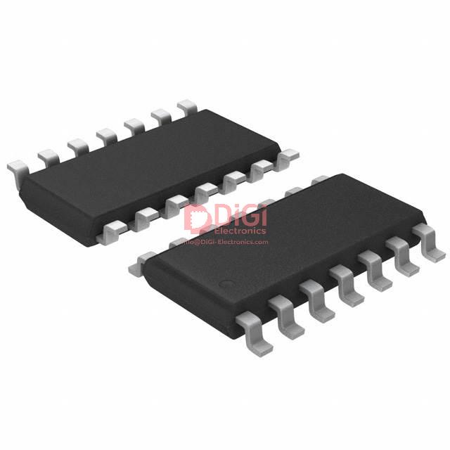
The 74HC393D utilizes a 14-pin SOIC surface-mount package, directly conforming to JEDEC standards for outline dimensions, terminal pitch, and lead coplanarity. This uniformity is essential for automated pick-and-place systems, as it ensures reliable part recognition by vision systems and consistent soldering quality across high-volume productions. The device’s mass of approximately 0.13 grams proves advantageous for high-density, multilayer PCB designs where cumulative component weight directly impacts mechanical stress and board warp risk. Such low-mass packaging also facilitates compliance with dynamic environments, for instance, in handhelds or aerospace embedded systems, where vibration and acceleration loads are critical factors.
Dimensional tolerances and pad geometry closely align with mainstream PCB CAD libraries, minimizing the risk of soldering anomalies such as tombstoning or insufficient wetting. This compatibility accelerates design cycles, as engineers can leverage standardized land patterns without custom footprint development, reducing both prototype iteration time and potential for assembly errors. The mechanical layout, characterized by clear pin 1 marking and chamfered package corners, directly supports automated optical inspection and orientation verification in reflow processes, minimizing misplacement and subsequent downstream failures.
Industry-standard pin numbering and functional marking, in line with Toshiba and broader vendor practices, facilitate rapid device identification and orientation during both design and assembly phases. This predictability is particularly beneficial for teams managing variant bills of materials or working within distributed manufacturing ecosystems. The clear differentiation of the device code and batch traceability on the top surface further streamlines quality assurance and lot management, essential for maintaining traceability across multi-stage supply chains.
From a production engineering perspective, the robust packaging of the 74HC393D supports both lead-free and conventional wave or reflow soldering profiles, offering flexibility in process qualification without compromising thermal stability or coplanarity. Consistent performance under repeated thermal cycling and high humidity conditions has been observed in practice, supporting long-term reliability metrics such as FIT rate and mean time between failure (MTBF) modeling. This underscores the package's suitability for mission-critical applications demanding both mechanical resilience and electrical integrity over lifecycle extremes.
Incorporating components like the 74HC393D in a standard SOIC-14 not only streamlines supply chain logistics but also enables platform approach designs, where multiple logic functions can share common mechanical footprints for easier substitutions and upgrades. In summary, the detail-oriented, standards-based mechanical and packaging approach of the 74HC393D underpins accelerated engineering workflows and supports the stringent quality demands of modern automated manufacturing environments.
Potential Equivalent/Replacement Models for 74HC393D
Dual 4-bit binary counters, typified by the 74HC393D, form integral components in digital timing, frequency division, and event counting applications. When addressing supply fluctuations or pursuing cross-vendor standardization, identifying functionally equivalent models demands a granular approach that extends beyond superficial datasheet matching. Devices such as Texas Instruments’ CD74HC393 and SN74HC393, Nexperia’s 74HC393D, and ON Semiconductor’s MC74HC393ADR2G each encapsulate the requisite dual 4-bit counter topologies, yet diverge subtly in electrical, mechanical, and reliability parameters.
The process for equivalence verification begins at the characterization layer. Electrical specifications—operating voltage ranges, input logic thresholds, output drive strengths, and quiescent current—require tight alignment with incumbent tolerances, especially where timing precision or low-power regimes dominate system priorities. Propagation delay profiles and setup/hold time requirements become critical in high-frequency clocking designs; minute variances can drive ripple effects through synchronization schemes, necessitating bench validation under representative load and temperature conditions.
Package compatibility hinges on both physical footprint and lead arrangement. SMD variants such as the ‘D’ package embody industry-standard outlines, although not all manufacturers translate the pinout identically. Subtle pin function differences, package markings, and lead pitch may entail layout adjustment or refined assembly process controls. Overlooking ESD robustness or moisture sensitivity level is a frequent pitfall—these properties influence manufacturability and in-field longevity, especially in edge-case applications such as industrial automation, automotive electronic control units, or aerospace timing logic.
When integrating alternative models, qualification cycles are most effective when augmented with accelerated stress testing, targeting variables like supply voltage margins, switching noise immunity, and failure modes under extended thermal cycling. Observed in practice, a candidate counter can exhibit acceptable bench performance but reveal shifts in count fidelity or output levels after environmental conditioning, underscoring the merit of empirical reliability screening.
Pin-compatible options present apparent simplicity, yet optimal replacement selection involves forecasting long-term vendor support, potential for obsolescence, and alignment with automated optical inspection criteria. Leveraging multi-sourced components mitigates downstream supply risk and expedites cross-manufacturer certification, while harmonizing design libraries streamlines layout migration and procurement strategy.
Notably, the most robust engineering results arise from systematic evaluation of datasheet minutiae, layered with practical in-situ assessment. Optimization favors solutions where functional equivalence coincides with matched tolerances, consistent signal integrity, and proven reliability in both prototyping and production contexts. This approach not only assures seamless substitution but strengthens resilience against future supply chain volatility and design iteration cycles.
Conclusion
The architectural design of the 74HC393D centers around dual, independent 4-bit binary counters built using advanced CMOS logic. The device’s asynchronous reset and clock inputs are buffered, providing resilience against signal integrity issues common in dense, fast-switching environments. Schmitt-trigger input structures further enhance noise immunity, supporting robust operation even when interconnect conditions deteriorate—such as in extended temperature or electrically noisy industrial and automotive installations. Its wide supply voltage range (2V–6V) allows deployment across mixed-voltage domains without compromising switching thresholds, yielding reliable propagation characteristics under stringent power constraints.
Timing precision is achieved through tight control of propagation delays and minimal clock-to-output skew, enabling predictable division ratios and synchronization in pulse trains, frequency division, or event-counting applications. The package’s low profile facilitates integration on multilayer PCBs with high component density, minimizing parasitic capacitance effects that could degrade high-frequency performance. During practical deployment, consistent output drive strength and fan-out capability have supported direct interfacing with microcontrollers, FPGAs, and other standard logic families without requiring additional buffering, reducing system complexity and board real estate.
Transitioning to cross-vendor sourcing, subtle variations in input threshold voltages, output drive current, and pinout conventions must be verified when substituting equivalent parts. In field-tested designs, mismatches in reset logic or output impedance across manufacturers have occasionally manifested as elusive timing faults or unanticipated logic states at elevated clock rates. Pre-qualification through automated test scripts has proven effective to ensure compatibility before board spin or production release.
The 74HC393D’s blend of speed, power efficiency, and input protection sets a baseline for scalable digital counting circuits. Its dual-counter configuration supports parallel processing of multiple data streams or simultaneous multi-channel signal conditioning. By exploiting the device’s low power consumption profile, designers have achieved continuous operation in battery-powered instrumentation without sacrificing counting accuracy or long-term stability. In high-vibration automotive ECUs, the device’s immunity to false triggering and performance under voltage transients has proven critical.
A fundamental insight lies in leveraging the 74HC393D not only for standard counting but also as a building block for modular, reconfigurable logic systems. Its well-characterized parameters and extensive cross-compatibility with legacy TTL and modern CMOS logic foster rapid prototyping and scalable system expansion. When selection criteria prioritize predictable timing, supply chain flexibility, and high integration density, the 74HC393D consistently delivers in next-generation digital logic platforms.


