


 >
>


Product Overview: TMS320C31PQL60 Digital Signal Processor
The TMS320C31PQL60 represents a cornerstone in Texas Instruments’ 32-bit floating-point DSP portfolio, engineered to satisfy intensive signal processing requirements. At the silicon level, this device utilizes a 0.6 μm CMOS process, optimizing both power efficiency and speed, which are critical in minimizing latency and thermal challenges within compact embedded architectures. The floating-point arithmetic unit enhances precision and dynamic range in computational tasks, positioning the processor for scenarios where fixed-point limitations compromise fidelity—such as spectral analysis, filtering, and real-time control algorithms.
From a systems perspective, this DSP’s architecture combines a high-throughput data path with flexible peripheral integration, enabling streamlined communication with A/D and D/A converters, memory modules, and external bus interfaces. This extensive peripheral set, unified within a 132-pin BQFP, facilitates efficient PCB layout and reliable high-speed signal transfer without excessive board complexity. The native support for concurrent data and instruction flow counters the typical bottleneck effects in multi-stage digital signal chains, granting significant headroom for complex, iterative numerical computations.
Practically, the TMS320C31PQL60 is frequently found at the heart of industrial automation controllers, advanced imaging platforms, and telecommunications infrastructure equipment. Its deterministic instruction execution ensures predictable timing, a necessity in closed-loop motion controllers and high-resolution measurement systems, where jitter undermines performance. Experience shows that design cycles leveraging this DSP's rapid context switching and memory-mapped I/O capability can achieve both throughput and real-time responsiveness, reducing the risk of system overruns in time-sensitive signal paths.
Application development benefits from the mature toolchain and ecosystem that TI’s TMS320 family has cultivated, with optimized libraries and debugging support accelerating firmware bring-up and iterative optimization. Engineers gain the flexibility to balance code efficiency with development time, leveraging floating-point support to bypass the scaling and saturation headaches typical in fixed-point platforms. The result is an environment in which algorithm prototyping and deployment align more closely with theoretical models, streamlining transitions from simulation to embedded deployment.
Gleaned from integration projects, one core insight emerges: the TMS320C31PQL60’s value lies not only in compute density but in its orchestration of data movement, determinism, and system-level integration. This allows architects to unify preprocessing, filtering, and control algorithms within a single silicon footprint, reducing both BOM complexity and development risk—key considerations when longevity and maintainability are paramount. By aligning processor strengths with high-mix, reliability-driven application domains, the TMS320C31PQL60 demonstrates enduring engineering relevance in an evolving DSP landscape.
TMS320C31PQL60 Architectural Features and Innovation
TMS320C31PQL60 employs a purpose-built hardware architecture, streamlining digital signal processing workloads through tightly coupled resources and novel instruction sequencing. At its foundation, the device integrates an advanced internal bus structure that efficiently interconnects core arithmetic elements and memory blocks, minimizing data transfer latency and promoting concurrent execution. This internal busing enables the parallel operation of the multiplier and ALU, crucial for high-throughput DSP routines where integer and floating-point operations must coexist within strict cycle budgets. By supporting simultaneous calculation across multiple data types in a single tick, the processor achieves significant acceleration over conventional sequential architectures.
Instruction set optimization is pivotal. The architecture features two- and three-operand instructions, allowing flexible manipulation of operands and results directly in register space, which prevents bottleneck issues commonly seen in memory-bound designs. Block repeat modes and zero-overhead looping empower engineers to implement iterative algorithms—FIR filters, convolutions, correlators—without incurring cycle penalties from loop control, thus preserving processing bandwidth for real computation. Conditional branching and interlocked instructions bolster control flow reliability, critical for adaptive filtering, decision-driven modulation, and real-time control logic that must respond dynamically within deterministic time constraints.
The dual address generator subsystem is engineered for rapid, non-sequential memory access. This design proves essential when handling data streams or implementing sliding window techniques, where simultaneous access to multiple memory locations is required during each cycle. Extended-precision registers enlarge the dynamic range and accuracy, which is paramount when cascading arithmetic operations, such as FFT stages or accumulation-focused algorithms susceptible to rounding errors. Auxiliary register arithmetic units (ARAUs) further reduce overhead in pointer calculations and address manipulations, expediting the management of circular buffers and matrix traversals frequently encountered in multi-dimensional signal processing.
In practice, leveraging these features allows for robust system integration. For example, block repeat modes with dual address generators translate directly into reduced instruction fetch cycles and deeper pipeline utilization when deploying DSP kernels in imaging or sensor fusion tasks. Careful register management and strategic use of the instruction set minimize memory bottlenecks while supporting deterministic interrupt handling, a necessity in high-reliability embedded applications such as precision measurement or motor control.
Key to the TMS320C31PQL60’s sustained relevance is its balance between low-level flexibility and high-level abstraction. The device provides granular architectural hooks that cater to both rapid prototyping and optimized product deployment, with hardware mechanisms that absorb many traditionally software-driven overheads. By implicitly facilitating parallelism, deterministic execution, and memory-efficient operations, the processor becomes especially suited for adaptive real-time systems, pushing the frontier in specialized DSP implementations. This architectural philosophy exemplifies how targeted hardware innovation can extend the limits of embedded signal processing, with practical design choices shaping fundamental capabilities.
Performance Specifications and On-Chip Resources of TMS320C31PQL60
Engineered for demanding real-time signal processing, the TMS320C31PQL60 leverages a 60 MHz pipeline, with each instruction executing at an efficient 33 ns cycle. This architecture directly yields a computational bandwidth of 330 MOPS, tightly matched to 60 MFLOPS for floating-point intensive tasks, and 30 MIPS for control-oriented workloads. The harmonized interaction between scalar throughput and floating-point acceleration enables predictable system response and sustained operational integrity under dynamic signal conditions.
Central to its resource allocation are the 2 × 1K × 32-bit single-cycle dual-access RAM blocks. This memory architecture eliminates bottlenecks by supporting simultaneous data read/write from independent buses, greatly reducing contention in time-critical algorithms such as digital filtering or transform computations. The rapid access patterns, in conjunction with the on-chip 64 × 32-bit instruction cache, minimize latency spikes, sustaining high-frequency algorithm loops and lowering the probability of stalls on instruction fetches. This cache design is particularly beneficial in application profiles marked by repeated execution of computation kernels, as seen in real-time control loops and DSP algorithm modules.
The CPU core, implemented as a 32-bit datapath, integrates a high-speed multiplier and a barrel shifter. This foundational approach to instruction-level parallelism allows multi-operand mathematical operations to complete within single cycles—a requirement when harmonizing digital signal flows or running matrix multiplications common in image and spectral analysis. The embedded barrel shifter is instrumental for scaling and normalization, rapidly managing data ranges in fixed- and floating-point math, thus enhancing numeric stability in large dynamic range environments.
On-chip peripheral integration is executed with practical flexibility. The serial port supports synchronous and asynchronous communication schemes, directly fitting into audio codec interfacing, multiplexed sensor acquisition, or point-to-point digital communication architectures. Real-world interaction with external modules is simplified by programmable framing and baud rate control, removing the burden of external glue logic and streamlining hardware-software interfacing.
Temporal coordination is provided by two independent 32-bit timers, which serve dual purposes in periodic event generation and time-stamp tracking. In scenarios such as motor control or event sequencing in instrumentation, these timers afford fine-grained interval management without excessive software overhead, optimizing both predictability and interrupt latency.
The tight integration of a one-channel DMA controller further boosts system efficiency. It enables concurrent data streaming between memory and peripheral devices, decoupling data movement from CPU cycles. This configuration proves substantial in application domains where time-deterministic data harvesting and processing must proceed in parallel, such as in high-rate data logging or real-time sensor fusion.
Interrupt management and bus control features extend the chip’s versatility by simplifying task prioritization and supporting seamless integration into complex multiprocessor clusters. Multi-level interrupt handling ensures rapid response to asynchronous events, maintaining deterministic performance even in systems characterized by frequent context switches and distributed computation.
From hands-on deployment, the interaction between high-throughput RAM and cache structures surfaces as tactically important in optimization efforts. Code segmentation tailored to cache line boundaries and workload partitioning across RAM blocks often yields measurable gains in sustained throughput, especially when orchestrating multiple signal flows concurrently. Robust system engineering benefits from implicit support for modular expansion and multiprocessing, allowing designers to scale from stand-alone embedded devices to distributed real-time processing arrays without re-architecting core scheduling or communication layers.
Ultimately, the TMS320C31PQL60 demonstrates the value of balanced resource integration, where deterministic computational performance is underpinned by high-efficiency memory, tightly-coupled processing, and adaptive interfacing. This synergy fosters a predictable development process in precision-dependent signal environments, confirming both design reliability and long-term platform adaptability.
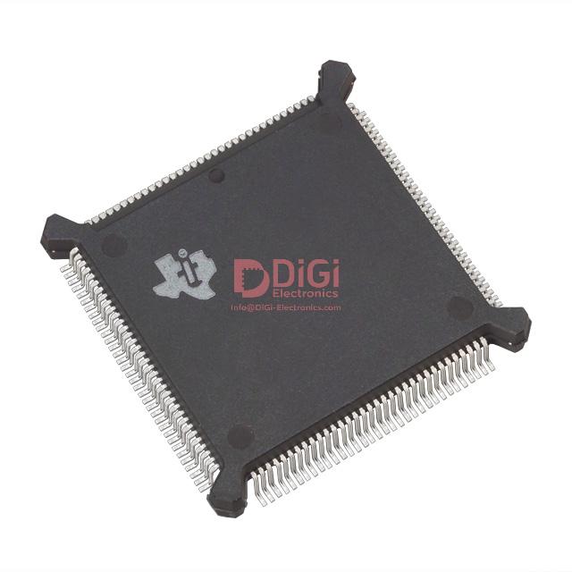
Package, Pinout, and Terminal Assignments for TMS320C31PQL60
The TMS320C31PQL60 integrates system functions within a 132-BQFP (24.13 × 24.13 mm) format optimized for surface-mount applications. The package’s rigid construction maintains coplanarity, supporting high-frequency operation and thermal dissipation. Pin distribution strategically accommodates core processor interfaces: a dedicated allocation for data and address buses ensures low-latency memory access and streamlined peripheral communication. Control signals, distributed across the package, minimize cross-talk and enable deterministic state management for real-time processing scenarios.
The pinout reflects a deliberate system-level partitioning. Power and ground assignments are concentrated to create a low-impedance path, reinforcing signal integrity while simplifying layer stackup in multilayer PCBs. EMU lines for JTAG-based emulation and debugging are isolated from high-speed signal clusters, reducing the risk of unintended interference during in-circuit testing or firmware deployment. The reservation of initialization-specific terminals contributes to reliable boot sequences and guards against floating nodes, a subtle design feature that mitigates erratic startup behaviors observed in high IO-density devices.
Terminal assignments are referenced numerically and alphabetically, facilitating schematic capture workflows and reducing ambiguities in component placement and routing. This dual-order system supports automation and error checking during design verification, a critical layer for complex boards where dense BQFP packaging could otherwise obfuscate signal tracing. The explicit grouping of functional pins—such as clock domains, bus interfaces, and peripheral access—enables modular design strategies and expedites iterative layout revisions.
Design experience reveals that careful management of ground return paths and proximity of decoupling capacitors to supply pins markedly improves transient response and mitigates EMI issues, particularly in DSP-intensive environments. Pinout transparency directly benefits high-speed trace design and bus arbitration logic, streamlining signal timing analysis and physical implementation. Strategic placement of reserved pins provides insurance against future hardware modifications, allowing incremental enhancements without full board spins or risking signal integrity.
Analysis of pin assignment conventions across similar DSP families indicates that the TMS320C31PQL60’s approach, which maintains clear separations and avoids multiplexed configurations for critical signals, establishes a stable foundation for predictable board bring-up. A nuanced understanding of the interaction between package mechanics and circuit topology reveals opportunities to harness EMI shielding and leverage plane assignment for robust, low-noise performance.
In deployment, these mechanisms collectively contribute to confidence in system reliability and design scalability. When rapidly iterating board designs or troubleshooting faults, the clear organization and robust assignment logic minimize downtime and isolate root causes quickly, evident in reduced time-to-market and sustained operational integrity in diverse applications ranging from industrial controls to embedded instrumentation.
Peripheral Interfaces and Control Signals in TMS320C31PQL60
The TMS320C31PQL60 architecture integrates a diverse suite of peripheral interfaces engineered for robust performance across varied digital signal processing environments. At its foundation, the processor employs a 32-bit primary data port (D31–D0) and a 24-bit address bus (A23–A0), ensuring ample bandwidth for high-speed, parallel access to memory arrays and peripheral devices. This direct interfacing capability minimizes latency, critical in real-time control systems and high-throughput data pipelines.
Central to deterministic system operation are its comprehensive control signals. The R/W line secures explicit management of memory and peripheral operations; coupled with the STRB signal, precise timing of data transactions is achieved. The RDY input serves a vital role in coordinating external bus cycles by signaling transaction completion, effectively managing wait states, particularly when chaining slower external memories. HOLD and HOLDA signals are indispensable for shared bus arbitration, facilitating seamless DMA operations or multi-processor configurations without contention, supporting modular expansion and system resilience in industrial setups.
Four prioritized interrupt inputs (INT3–INT0) empower responsive event handling, facilitating preemptive multitasking and granular real-time adjustments, especially where latency to asynchronous events—such as sensor triggers or communication packets—is non-negotiable. In practice, fine-tuning of interrupt priority and vector assignments accelerates exception handling and error recovery.
Integrated synchronous serial communications are realized through CLKX0/CLKR0 (transmit and receive clocks), DX0/DR0 (serial data lines), and FSX0/FSR0 (frame synchronization). This configuration streamlines interfacing with industry-standard codecs, ADCs, and DACs, permitting jitter-free audio/video acquisition and transmission. Adhering to precise clocking patterns and frame alignment during site deployment mitigates skew and data integrity issues, especially in multi-channel, high-fidelity systems.
External flag pins, XF0 and XF1, provide versatile functions as general-purpose I/O or instruction synchronization markers. For instance, using XF0 to signal firmware update completion or pipeline synchronization between co-processing units can reduce overhead from polling mechanisms. Their deployment in signaling custom protocol states or synchronization points introduces system-level flexibility without additional hardware complexity.
Timer signals TCLK0 and TCLK1 afford modular timing reference generation, integrating seamlessly with both external clock sources and internal routines. Application scenarios benefit from using these inputs for event timestamping, pulse generation, or periodic interrupt scheduling. In environments demanding precise time base—such as motor control, process automation, or measurement instrumentation—the versatile timer architecture allows adaptation to both fixed-frequency and variable-rate requirements.
A unique observation: Optimally balancing between internal controller resources and external signal management not only enhances speed and reliability, but also reduces debugging overhead during integration phases. Carefully mapping peripheral assignments and exploiting the deterministic nature of control signaling often yields superior throughput and system stability, particularly in heterogeneous or mission-critical configurations. The layered interface logic of the TMS320C31PQL60 thus provides a solid foundation for scalable, high-performance embedded designs, supporting both rapid prototyping and mature deployment.
Power Supply, Clocking, and Low-Power Operation in TMS320C31PQL60
The TMS320C31PQL60 is engineered with a unified 5.0 V supply architecture, covering both the processor core and I/O domains. This commonality simplifies power distribution but elevates the need for careful implementation of supply integrity across all VDD and VSS pins. Ensuring each power and ground pin is bonded to broad, low-impedance planes mitigates voltage droop and supply noise during high-current switching, directly influencing DSP reliability and signal quality. Practical experience points to the measurable benefits of generous decoupling—placing an array of ceramic capacitors proximate to the device perimeter dramatically suppresses high-frequency transients induced by the processor’s computational bursts. Even minor inconsistencies in plane connectivity can manifest as increased ground bounce, affecting deterministic execution and analog interface stability.
Clocking Mechanisms for Precision Operation
Stable timing is foundational for high-throughput signal processing. The TMS320C31PQL60 facilitates direct interfacing to either a crystal element or an external clock source via X1 and X2/CLKIN. When in crystal oscillator configuration, minimizing loop area and guard-ring technique for crystal traces curbs EMI susceptibility, enhancing long-term timing precision. In scenarios prioritizing minimal clock drift or synchronization across multiple DSP nodes, injecting a tightly controlled external clock at CLKIN guarantees cycle alignment and meets stringent timing budgets. Signal integrity at the clock input is non-negotiable; ringing or overshoot on CLKIN leads to excessive jitter, which propagates unpredictability into the processor pipeline and subsequent peripherals. Applying parallel damping resistors and close-by terminations refines clock quality to the device’s level-sensitive input characteristics.
Low-Power Functionality and Mode Transitions
Energy management in compute-intensive platforms demands more than passive power supply design. The inclusion of two low-power modes supports dynamic power gating of internal blocks driven by operational context—enabling significant reduction in active power dissipation. These modes are especially advantageous in duty-cycled systems or scenarios where periodic idling is intertwined with signal acquisition or event-based triggering. Entry and exit from these modes must be orchestrated with precision: applying appropriate pull-ups and pull-downs on mode control and status pins stabilizes pin state, ensuring deterministic wake-up and re-initialization. Notably, improper biasing during mode transitions has been observed to sporadically latch the core in indeterminate states, underlining the mandate for explicit board-level design validation in all power states.
Test and Extreme Power Reduction Mode
Distinct from standard low-power operation, the SHZ-enabled test mode forcibly enters a deep current reduction state, primarily targeting in-system test validation where ultra-low current draw is essential for boundary scan or soak testing. This state is not intended for operational cycling during live workloads and must be isolated from main firmware logic to avoid adverse system hang conditions. An implicit but crucial insight is to gate SHZ entry with robust, non-glitch-prone logic, preventing inadvertent silicon disablement which complicates field recovery. PCB-level oversight, such as segregated trace routing and high-immunity input protection at the SHZ pin, further safeguards long-term deployment reliability.
Initialization, Pull-ups/Downs, and Robust Wake-up
System start-up and reset recovery are sensitive to pin configuration, particularly in DSPs where IO state at power-up defines functional domain boundaries. Applying appropriate pull-up or pull-down resistors on critical control lines establishes deterministic device behavior across power cycles and mode entries, safeguarding against metastable logic conditions and unintended peripheral activation. Experience indicates that the value selection of these resistors should balance between holding strength and reactivity; excessively strong pulls risk increased standby leakage, whereas insufficient biasing leaves the DSP susceptible to noise-induced initialization errors on exposed nets. Board and system validation cycles must encompass various power and wake-up scenarios to empirically confirm repeatable, robust operation.
From a design integration viewpoint, the tight coupling of power supply layout, clock trace topology, and stateful low-power logic forms its own system-level feedback loop; minor deviations in one domain can ripple through and impact total system performance. Employing layered validation—at schematic, layout, and in-system firmware levels—delivers consistent functional assurance, ultimately extracting maximal reliability and energy efficiency from the TMS320C31PQL60’s architecture within advanced signal processing platforms.
Memory Map and Bus Structure of TMS320C31PQL60
The TMS320C31PQL60 features a sophisticated memory organization designed for maximum adaptability across diverse embedded applications. The device operates under both microprocessor and microcomputer/boot-loader modes, enabling flexible use cases that range from streamlined system-on-chip designs to networked multiprocessor arrays. The memory map is architected for deterministic performance and robust exception management. At the foundation, dedicated regions store reset, interrupt, and trap vectors, ensuring reliable response to system control signals and asynchronous events with minimal latency.
Hardware resources are extensively addressable through peripheral-dedicated and memory-mapped register regions. This approach maximizes data throughput for on-chip devices and external interfaces, facilitating direct control and monitoring without superfluous instruction cycles. Embedded RAM is organized into two independent 1K-word blocks, supporting concurrent code execution and data manipulation. This duality optimizes critical routine isolation and reduces bus contention, a requisite for high-speed signal-processing algorithms. Practical deployment often leverages the separation to assign one block for near-time control data and the other for core algorithm code, minimizing access conflicts during pipeline execution.
External memory interfacing leverages wide STRB-validated addressable regions, supporting up to 8 megawords. The scalable mapping can articulate boot regions, user application branches, and reserved areas tailored to future system expansion or device-specific overlays. For complex products, this enables seamless in-field firmware updates and dynamic partitioning of resource space without hardware redesign. The boot memory region is especially valuable in environments requiring flexible startup routines, such as in systems supporting multiple boot images or secure authentication procedures.
The high-throughput parallel bus structure incorporates programmable bus-control registers, which are capable of generating fine-tuned wait states. This mechanism underpins compatibility with slower peripheral devices and heterogeneous external RAMs, allowing the processor’s speed to be decoupled from that of subordinate resources. Precise wait-state management provides significant engineering leverage when integrating varied legacy components, maintaining overall system timing without performance loss on critical paths. Advanced application scenarios, such as real-time signal acquisition or multi-stream data buffering, benefit from the deterministic bus behavior and the predictable peripheral handshake afforded by this bus system.
A core insight arises from the C31’s balanced approach to memory and bus design—the architecture intentionally avoids over-specialization, favoring a flexible configuration set that adapts to both legacy and emerging system requirements. The layered division between tightly-coupled internal RAM, broad addressable external memory, and configurable peripheral space creates a platform for scalable product families. System architects can exploit these layers to separate time-critical real-time operations from lower-priority programmability or legacy module support. In turn, this capability accelerates both initial development and subsequent field upgrades, yielding superior total system longevity and maintainability in industrial and embedded environments.
Environmental and Compliance Information for TMS320C31PQL60
Environmental and Compliance Considerations for TMS320C31PQL60 are foundational for risk-mitigated system integration. At the regulatory level, the device’s RoHS3 compliance and unaffected REACH status confirm its eligibility within markets requiring strict limitation on hazardous substances, reducing liabilities associated with environmental directives. These certifications signal supply chain stability and simplify multi-region deployment, eliminating the need for redesign or recertification due to shifting compliance landscapes—a common challenge in long-lifecycle embedded designs.
Classification data reveal the device aligns under ECCN 3A991A2 with HTS category 8542.31.0001. Such designations streamline export management, allowing controlled but flexible movement across jurisdictions. In practice, this enables agile logistics, reducing administrative overhead and potential shipment delays for international projects.
Moisture Sensitivity Level (MSL) 2A, corresponding to a four-week floor life, underpins robust handling protocols during PCB assembly. This MSL grants an optimal margin for modern surface-mount processes, preventing latent defects such as internal delamination or popcorning during reflow. Proactive moisture control in storage and staging areas further minimizes quality risk, evidenced in yields tracked by leading EMS providers.
The specified 0°C to 85°C case operational temperature window positions the TMS320C31PQL60 for widespread adoption in both controlled industrial floors and embedded environments with moderate ambient variation. Notably, this range accommodates scenarios where cabinet climate control may be present but not absolute, such as light manufacturing, commercial automation, and telecommunications. Field deployments leveraging this DSP typically exhibit high MTBF owing to its conservative thermal regime; however, attention to system-level derating and heat dissipation remains prudent, particularly in dense assemblies or applications with sporadic thermal cycling.
These compliance and qualification attributes converge to create a component profile optimized for efficiency-driven, globally deployable platforms. When specifying TMS320C31PQL60, design assurance is enhanced by the alignment of international environmental standards and streamlined logistics. This harmonious balance reduces friction in both procurement and long-term support, allowing engineering efforts to remain focused on domain-specific innovation rather than regulatory risk management.
Potential Equivalent/Replacement Models for TMS320C31PQL60
When addressing obsolescence of the TMS320C31PQL60, careful mapping of its system role and subsystem constraints is essential before selecting equivalent parts within the TMS320C3x or TMS320LC31 families. The TMS320C31-80 delivers a direct architectural continuation, leveraging a higher 80 MHz clock at the standard 5 V supply, which broadens processing bandwidth for computation-heavy digital signal processing workloads. Applications dependent on deterministic real-time execution—such as motor control or adaptive filtering—may benefit from this headroom, provided core and peripheral timing margins are validated across the software stack and physical design.
For scenarios where power budgets or thermal limits are more stringent than raw throughput requirements, alternatives like the TMS320C31-50 and TMS320C31-40 maintain functional and pin compatibility with their 5 V operation, allowing drop-in replacement for legacy boards without significant PCB or power redesign. However, awareness of their clock-specific instruction cycles is crucial: time-critical loops may require retuning, and peripherals clocked directly from the DSP may need recalibration due to altered cycle counts.
Moving toward the TMS320LC31-40 and TMS320LC31-33 shifts supply levels down to 3.3 V, which favors mixed-voltage or battery-operated systems. While these devices retain an instruction set and most peripheral intersections, digital core thresholds and I/O margin must be carefully matched against existing logic families to avoid signal integrity issues. Board-level considerations include level shifters or redesign of associated analog front-ends, particularly for high-speed ADC/DAC signal paths or communication with 5 V-only transceivers.
Key system constraints such as package type, available peripherals, and the memory mapping architecture require explicit cross-verification. A common pitfall in field upgrades stems from overlooking subtle differences in onboard SRAM size, bootloader setup, or DMA arbitration priority, which may surface only during stress-testing or with large codebases. Developing a standardized evaluation protocol that benchmarks critical execution paths, interrupt latencies, and I/O compatibility ensures smooth migration and minimizes post-deployment surprises.
In legacy DSP modernization efforts, voltage rail congruence and thermal envelope management often prove more limiting than code or pinout compatibility. Integrating replacement analysis upstream in lifecycle planning, and maintaining a parallel validation platform, can de-risk conversion bottlenecks and extend system viability—particularly in long-lived industrial control, test equipment, and legacy instrumentation. This layered approach optimally balances immediate form-fit-function needs with future-proofing flexibility, supporting robust DSP migration strategies in evolving application environments.
Conclusion
A close examination of the Texas Instruments TMS320C31PQL60 DSP reveals a robust architectural foundation designed to meet the exacting demands of high-throughput embedded signal processing. Central to its effectiveness is the hardware-oriented implementation of a 32-bit floating-point arithmetic unit, which allows rapid execution of complex mathematical operations essential for real-time filtering, control, and data transformation workflows. The processor’s direct memory access channels, multiple external memory interfaces, and modular I/O peripheral integration collectively streamline system-level data flows, minimizing latency across computational and communication boundaries.
Signal integrity and data reliability remain critical concerns in embedded design, and the TMS320C31PQL60 addresses these through precise pinout mapping and carefully balanced power distribution heuristics. Its on-chip clock management and support for synchronous/asynchronous bus configurations facilitate fine-tuned timing control, which proves beneficial in scenarios where deterministic response—such as in active noise cancellation, precision industrial controllers, and high-fidelity audio pipelines—is non-negotiable.
Effective utilization hinges on thorough familiarity with its internal register structures, interrupt handling routines, and memory map flexibility. Engineers regularly benefit from this layered memory organization, leveraging segmented RAM, ROM, and mapped peripherals to optimize real-time performance while constraining latency within predictable bounds. Critical application domains—legacy radar processing, digital servo loop management, and medical imaging analysis—demonstrate measurable gains when exploiting the DSP’s concurrent computation resources and peripheral co-processing capabilities.
In transition planning for system obsolescence or migration, sustained value lies in the clarity and transparency of the TMS320C31PQL60’s documentation. Efforts to support legacy installations are expedited by well-established benchmarks and compatibility matrices, ensuring that evaluation and onboarding of next-generation TI DSPs incorporate both hardware/software interoperability and forward-looking design scalability. Subtleties in pinout configuration and voltage sequencing directly influence retrofit scenarios; domain-specific testing reveals that small modifications to clock edges or bus width settings can yield marked improvements in stability and throughput when integrating new modules.
The device’s historical dominance underscores a broader insight: longevity in signal processing architecture is anchored less in transient specifications and more in modularity, extensibility, and granular control over data paths. This perspective guides modern selections, emphasizing architecture-first thinking over superficial feature comparison. The TMS320C31PQL60 remains a reference point for pragmatic signal processing hardware, representing a set of design principles that current and future embedded solutions can adopt and refine to accelerate engineering workflows without compromising operational integrity.


