 >
>


Product Overview of SN74ACT7802-25FN
The SN74ACT7802-25FN delivers robust FIFO buffering capabilities aligned with the requirements of high-throughput data systems. Built on advanced CMOS logic, its core structure minimizes propagation delay while maintaining low power consumption, critical for board designs prioritizing both speed and efficiency. The device’s 1K x 18-bit organization enables seamless handling of wide, parallel data streams—a foundational requirement in digital signal processing, telecommunications, and high-bandwidth bus arbitration. By occupying a 68-pin PLCC package, it supports straightforward integration into complex multi-layer PCB layouts, ensuring reliable interconnects and signal integrity for dense system environments.
At the architectural level, the SN74ACT7802-25FN implements asynchronous read and write control mechanisms. This decoupling of input and output operations enables rate-matching between disparate functional blocks without necessitating a global clock domain. Such design increases system flexibility and mitigates metastability risks in heterogeneous digital platforms. The device’s full and empty status flags, combined with independent data valid indicators, simplify hardware state management, granting designers granular visibility into buffer states and allowing for fine-grained flow control at the interface level.
Application scenarios for the SN74ACT7802-25FN range from buffering real-time video streams to acting as protocol bridges in backplane communication infrastructures. The device efficiently addresses bursts from high-frequency sources, absorbing excess data and releasing it downstream at controlled rates. This capability is particularly valuable in modular embedded systems, where timing disparities between processor subsystems would otherwise introduce bottlenecks or data loss.
In implementation, attention to signal timing and proper board decoupling remains key. The wide I/O bus and substantial input capacitance demand careful PCB trace routing and ground plane strategies to prevent crosstalk and voltage sag. Power supply stability, safeguarded by localized bypass capacitors, is instrumental in preserving switching fidelity across the FIFO under variable loads. These board-level practices, combined with synchronous reset management and signal edge conditioning, maximize device reliability.
Unique among FIFO memories, the SN74ACT7802-25FN’s asynchronous control logic paired with wide word support distinguishes it as a strategic buffer solution for emerging architectures that must bridge legacy and modern data standards. The combination of high word width and rapid access time opens new pathways for interfacing between serial-to-parallel converters and DSP arrays, supporting scalable bandwidth growth without sacrificing backward compatibility. This positions the part as not only a drop-in buffer but as a forward-looking component for adaptive system architectures targeting next-generation performance benchmarks.
Core Functional Features of SN74ACT7802-25FN
The SN74ACT7802-25FN FIFO integrates a robust asynchronous architecture, enabling decoupling of write and read processes through independently clocked load (LDCK) and unload (UNCK) controls. This core feature effectively resolves the challenge of clock domain crossing, which often arises when integrating heterogeneous digital subsystems. Asynchronous FIFOs like this device provide deterministic data handoff, mitigating metastability issues inherent in synchronous bridges and preserving data integrity across divergent operational frequencies.
Operational performance is a critical differentiator for the SN74ACT7802-25FN. The device delivers up to 40 MHz data rates with low access times of 30 ns (tested under 50-pF loading), placing it within the class of FIFOs suitable for real-time data buffering in demanding digital pipelines. The low access latency directly contributes to reduced cycle stalls in high-performance applications, such as real-time image acquisition chains or multiplexed signal processing blocks, where data throughput consistency is paramount.
A distinctive mechanism is embodied in the fall-through time specification. Following a reset and a single load-clock edge, the first stored word appears on the output after only 20 ns, independent of explicit read operations. This behavior facilitates rapid pipeline priming; for instance, immediate availability of initialization vectors in DSP architectures or expediting live data pass-through in telecom switching nodes. The ability to instantly access the first data word streamlines buffer loading and can be leveraged in systems that require minimal buffer fill latency right after startup or a flush event.
Output interfacing is engineered for maximal system compatibility. The high-drive, three-state outputs permit direct connection to shared data buses, ensuring that only the selected FIFO instance drives the common lines, lowering bus contention probability. Practical design experience underscores that three-state management is instrumental when employing cascaded FIFOs or shared parallel bus fabrics. The pin-compatible expandability supports transparent width scaling by paralleling multiple devices, which is particularly advantageous in the context of scalable multimedia backplanes or wide-word telecommunication aggregators.
In application, the SN74ACT7802-25FN bridges the gap between clock-divergent subsystems, ensuring that high-speed data transport does not suffer from the traditional pitfalls of timing uncertainty. Unique architectural provisions like rapid fall-through and three-state logic, when employed in thoughtfully segmented designs, enable scalable and resilient data highways that adapt to evolving bandwidth requirements. Advanced users can exploit these features for system architectures requiring both speed and robust handshaking, positioning this FIFO as a versatile solution for contemporary digital system integration.
Electrical Characteristics and Timing Specifications of SN74ACT7802-25FN
Electrical characteristics of the SN74ACT7802-25FN are rooted in the device’s advanced CMOS implementation, enabling it to maintain precise voltage thresholds while minimizing leakage currents and dynamic power loss. The 5 V single-supply operation streamlines system integration with legacy and modern logic families, offering a stable ground for signal referencing. Input and output voltage parameters are tightly bounded, supporting both logic high and low levels for optimal noise margins. On the output side, the robust drive capability ensures stable logic states across varying capacitive loads, which is essential for high-fidelity signal transmission in complex circuit topologies.
Delving into timing specifications, the 30 ns access time defines the upper boundary for word retrieval latency, a factor that directly influences system throughput in high-speed digital applications. The architecture emphasizes a rapid fall-through response—20 ns post-reset—reducing dead-time during initial buffer load. This swift initiation is especially advantageous for designs requiring deterministic startup or frequent context switching, such as in real-time data acquisition or protocol bridging. Supported data rates approach 40 MHz, permitting seamless operation in systems with demanding bandwidth requirements. Internal timing paths are optimized through balanced clock distribution and finely tuned data latching, minimizing skew and clock-to-output uncertainty. These attributes permit tighter timing closure in synchronous pipelines and reduce the risk of setup/hold violations under variable load conditions.
Thermal management is addressed at both component and system levels. With a 39°C/W thermal impedance for the PLCC package, designers can predict junction temperature rises under worst-case switching scenarios. This specification is instrumental in multi-device PCB environments where spatial density can exacerbate thermal gradients. Empirical tests reveal that conservative placement of bypass capacitors near supply pins, combined with ground plane optimization, further stabilizes transient response and mitigates potential for localized overheating. Such thermal-aware design practices extend device longevity and preserve timing fidelity, especially under sustained high-frequency operation.
A critical insight is that the balance between speed and signal integrity hinges not only on intrinsic device characteristics but also on external board-level practices. The SN74ACT7802-25FN’s electrical tolerances and temporal precision are best leveraged when complemented by controlled impedance routing and disciplined power delivery networks. When deploying the component in large-buffer chains or high-fanout scenarios, careful signal timing simulation and proactive crosstalk mitigation become key to maintaining error-free communication cycles.
In summary, the SN74ACT7802-25FN’s electrical and timing landscape offers a high degree of design confidence, supporting both aggressive data throughput and sustained operational reliability. Its synergy with disciplined PCB layout and thermal strategy allows for robust application in digital buffering, data multiplexing, and protocol conversion, even in electrically and thermally aggressive system environments.
Flag and Status Systems in SN74ACT7802-25FN FIFO Memory
Robust FIFO buffer management requires granular, real-time state awareness, and the SN74ACT7802-25FN addresses this through an integrated set of hardware flag outputs. Each flag is engineered for tight coupling with system logic, enabling deterministic flow control in high-reliability digital pipelines.
The FULL flag asserts low precisely when the FIFO reaches a depth of 1024 words, providing immediate hardware feedback to disable further writes. This is a vital safeguard for asynchronous or high-throughput interfaces, especially where latencies between write intent and acknowledgment could introduce overflow risks. Conversely, the EMPTY flag asserts low only when the last valid word has been read, serving as a definitive handshake for read operations and ensuring data coherence in multi-clock or bidirectional transfer architectures.
Beyond these binary edge conditions, the HALF-FULL (HF) flag gives mid-level granularity, toggling high once 512 or more locations are occupied. This midpoint signal has distinct utility in scenarios demanding predictive prefetching or staged resource allocation—enabling, for instance, throttling or preemptive buffer draining based on system thresholds well before hard limits are encountered.
The programmable Almost-Full (AF) and Almost-Empty (AE) flags allow for flexible buffer monitoring far more nuanced than fixed trip-points. These user-specified thresholds facilitate tailored interrupt or DMA triggers. Experience in real-world systems demonstrates that placing AF at 90% and AE at 10% often strikes an optimal balance between maximizing buffer utilization and minimizing the risk of boundary violations due to bursty or uneven traffic. The programmable logic underlying these flags integrates seamlessly with hardware state machines, supporting both periodic polling and asynchronous, interrupt-driven architectures without imposing additional firmware load or timing uncertainty.
The deterministic nature of these status outputs is fundamental for implementing hardware-managed flow control. By wiring flags directly into device enable signals or microcontroller interrupt lines, one achieves immediate response to critical events—essential for maintaining data integrity in real-time sensor aggregation, data acquisition systems, or network buffering where any latency or mismanagement propagates downstream errors or losses. Notably, in designs where precise timing is less critical, these same flags support adaptive software algorithms, offering the flexibility to scale between hard real-time and best-effort buffering models.
Analyzing deployed applications reveals that the most resilient designs leverage status flag combinations rather than relying on a single boundary indicator. For example, pairing the HF mid-level alert with the AF near-capacity trigger allows dual-tiered throttling strategies, improving overall throughput while reducing stall intervals. In tightly-coupled multi-FIFO chains—such as those found in networking hardware or embedded DSP streams—correct interpretation and timely use of these hardware flags often demarcate high-performance, lossless designs from those prone to intermittent faults under stress.
In summary, the SN74ACT7802-25FN’s flag and status system constitutes a finely-tuned bridge between hardware-level buffer state and system-wide data integrity policies, offering both flexibility and precise control over memory-bound data flows. Meticulous integration of these signals within the overall system architecture consistently yields greater resilience and throughput in complex, high-demand applications.
Programming the Almost-Full/Almost-Empty Flag in SN74ACT7802-25FN
Programming the Almost-Full/Almost-Empty (AF/AE) flag in the SN74ACT7802-25FN enables precise management of data buffer states, especially in systems experiencing non-uniform or bursty data patterns. Fundamentally, this FIFO's AF/AE feature centers on a user-configurable threshold, settable via an offset value X. This mechanism allows the system to assert the AF/AE flag before the buffer actually transitions to completely full or empty, establishing an early warning point that assists in maintaining continuous, reliable data throughput.
At the hardware interface level, programming the AF/AE boundary diverges from default operation. By design, the factory-set threshold is positioned at 256 words. To override this default, specific manipulation of the DAF (Data-available Flag) and RESET signals is required during power-up or system re-initialization. Lowering the DAF input while asserting RESET low, followed by a positive transition of the RESET signal, registers the desired offset. This initialization sequence precisely defines where the AF/AE flag will trigger relative to the actual buffer occupancy. Implementation demands careful timing and noise management, as improper signal control can result in indeterminate thresholds or sticky AF/AE states—issues sometimes observed in multi-board systems with asynchronous resets.
In practical deployment, this feature introduces significant headroom for systems to react preemptively. For example, in high-throughput data acquisition chains or network packet buffers, setting a conservative AF threshold gives downstream processing blocks ample lead time to throttle inputs or offload data, thereby mitigating the risk of buffer overflow. Conversely, a similarly configured AE flag allows upstream logic to resume data transmission before starvation occurs. These techniques become especially valuable when integrating heterogeneous processing elements with mismatched I/O rates, as the flexible AF/AE trigger supports adaptive backpressure strategies.
Designers commonly iterate the threshold value during prototyping, calibrating the offset based on observed data rates, transaction latencies, or signal integrity margins. Finding the optimal value often demands a holistic view—factoring in not only average throughput but also worst-case jitter, clock domain crossings, and propagation delays. Undershooting the threshold may lead to unnecessary system stalls or throughput degradation, while setting it too close to the buffer limits reduces the cushion for real-time correction. Experience demonstrates that a dynamic, scenario-driven configuration—sometimes even modifying X according to operational context—delivers robust performance across diverse application domains.
A key insight is that the programmable AF/AE flag serves not merely as an indicator, but as an active control mechanism in distributed or deeply pipelined designs. Leveraging it as an actuator within flow control algorithms substantially enhances system agility, transforming static buffers into intelligent, self-regulating components. The value realized thus extends well beyond data protection, directly influencing the efficiency and reliability of entire data handling pipelines.
Package and Integration Considerations for SN74ACT7802-25FN
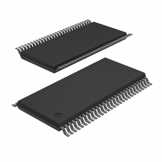
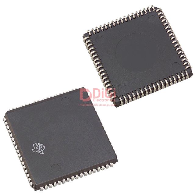
The SN74ACT7802-25FN is optimized for advanced system designs requiring efficient memory buffering and interface logic, presented in a 68-pin PLCC (24.23 mm x 24.23 mm) and an alternative thin quad flat package. These footprint options are tailored for PCB layouts prioritizing high component density and minimal board space without compromising signal integrity or mechanical robustness. The PLCC format, with its J-lead configuration, enhances solder joint reliability and withstands thermal cycling, important in mission-critical or long-life-cycle applications.
At the hardware design level, the SN74ACT7802-25FN is engineered to support word-width expansion by allowing the parallel operation of multiple devices. This feature is critical for architectures requiring increased data path width, such as 32- or 36-bit-system buses, commonly found in digital signal processing or high-speed computation applications. The integrated configuration as demonstrated in practical 1024 x 36-bit buffer staging allows designers to scale the data interface width while maintaining uniform timing and minimal propagation delay, critical for synchronous memory and bus operations. Proper alignment of control signals, especially output enables and write strobes, ensures predictable parallel device interaction and avoids data contention on shared buses.
However, the internal address management design of the SN74ACT7802-25FN restricts the ability to achieve depth expansion by traditional cascading. Unlike some FIFO designs, chaining the devices to extend buffer length is not natively supported due to lack of dedicated look-ahead or serial-out cascading logic. This design characteristic mandates that overall buffer depth in an application is fixed by the capacity of a single device or parallel bank, thus shifting a greater share of memory management duties to system logic and potentially external controllers. In multi-device deployments, this limitation has broader impact on system resource allocation, as it may demand more sophisticated control state machines or necessitate hybrid buffering solutions mixing FIFO and RAM approaches.
Application scenarios benefit from this device when strict data path width requirements supersede the need for deeper buffering, as in network packet typing, video scan-line processing, or protocol bridging that require streamlined parallel transfers. When integrating the device, signal routing must minimize skew across parallel devices, and power supply decoupling should be distributed to suppress switching noise—particularly relevant when all devices in a parallel array toggle simultaneously under burst operation. Empirical observations indicate that closely matched PCB trace lengths and diligent layout of supply rails markedly improve signal fidelity and overall stability in dense configurations.
The architectural decisions embodied by the SN74ACT7802-25FN—prioritizing width scalability over depth—enable predictable, high-throughput data flow in tightly managed system environments. Carefully weighing these strengths and constraints supports effective integration and maximizes utility in designs where horizontal scaling aligns with core performance requirements.
Potential Equivalent/Replacement Models for SN74ACT7802-25FN
Identifying robust equivalent or replacement models for the SN74ACT7802-25FN hinges on a granular analysis of both functional architecture and electrical interfaces. The core selection criterion revolves around matching the FIFO configuration; this encompasses data width, total capacity, and flag architecture. Devices within the same family, such as Texas Instruments' Widebus™ FIFO series, often present variants with altered word widths or storage depths. For example, the SN74ACT7801 line, though offering a narrower data path, follows similar timing protocols and control approaches, facilitating engineered trade-offs when bus width can be adjusted at the system level.
Critical assessment of third-party alternatives extends beyond headline specifications, requiring close examination of flag programmability and the architecture of status signaling. Variations in programmable flags—such as full, empty, or half-full indicators—can significantly impact FSM or state-driven designs. Pinout congruence is also essential; while JEDEC standards govern most multi-word FIFOs, subtle discrepancies persist in output enable logic, active-low flag assertion, or unused pins. Cross-referencing package drawings with layout footprints avoids costly PCB redesigns or assembly issues.
Data rate and access timing are technical focal points in compatibility analysis. The SN74ACT7802-25FN’s ACT family pedigree typically supports faster access times and enhanced switching characteristics, thanks to CMOS logic advancements. Replacement devices must demonstrate comparable maximum input-to-output propagation and minimal access latency, especially under worst-case process–voltage–temperature conditions. Buffer performance can degrade due to cumulative tolerances; therefore, empirical board-level timing margin validation is recommended following device substitution.
Voltage and temperature ratings often appear harmonized across modern FIFO offerings, yet supply voltage tolerances and extended industrial temperature support can diverge, particularly among legacy or cost-optimized variants. Output drive strength further differentiates candidates—sufficient drive is essential for maintaining bus integrity without necessitating external line drivers, especially in larger or multi-drop systems.
Practical integration experience emphasizes the advantage of pre-qualifying replacement devices through parallel prototyping. Minor differences in control logic response or setup/hold requirements may manifest only during in-circuit operation. Additionally, industry shifts toward lead-free or RoHS-compliant packaging can influence thermal profiles during solder reflow, making process reproducibility a nontrivial concern.
A nuanced viewpoint is that relying on precise datasheet parity alone is insufficient for mission-critical or high-speed systems. Layered validation, incorporating both schematic and signal integrity simulation, is crucial. As semiconductor lifecycle volatility increases, favoring pin-compatible parts with documented migration paths and vendor assurance of long-term supply mitigates obsolescence risk, preserving design investment and system reliability.
Conclusion
Texas Instruments’ SN74ACT7802-25FN embodies a purpose-built FIFO memory architecture optimized for high-speed, low-latency buffering of parallel data in advanced digital systems. The device’s asynchronous dual-port structure supports independent read and write clock domains, allowing seamless interfacing with subsystems operating at disparate frequencies. This enables resolved timing bottlenecks and guarantees data integrity across varying operational scenarios, a fundamental requirement in complex embedded designs and high-throughput signal processing chains.
Central to the SN74ACT7802-25FN’s adaptability is its programmable flag logic, which provides customized indicators for programmable threshold levels such as full, empty, and near-full states. These features facilitate fine-grained flow control in systems where fluctuating data rates or unpredictable bursts necessitate real-time buffer status signaling. With robust asynchronous control, the device efficiently coordinates data movement even in scenarios involving handshaking between heterogeneous modules or bridging legacy and modern protocols.
Integration within system architectures demands careful attention to timing margins, board layout, and power sequencing. The device’s CMOS-compatible logic minimizes contention on shared buses, while its low propagation delay ensures that it can sustain sustained data streams without incurring bottlenecks. Experience shows that, in data acquisition modules and networking equipment, precise configuration of programmable flags alongside tight PCB trace routing directly impacts overall throughput and timing closure. Underrating these factors tends to result in metastability or unintended data loss—demands which push engineers toward rigorous signal verification at both schematic and layout stages.
The SN74ACT7802-25FN proves particularly effective in scenarios where deterministic latency and robust buffer management underpin system reliability—such as FPGA front-ends interfacing with wide data buses, packet buffering in Ethernet switches, and real-time video or audio processing pipelines. Each deployment scenario tends to impose unique constraints. Selecting optimal device parameters and integrating programmable attributes into system firmware becomes a decisive engineering challenge. Observed in production environments, the strategic use of programmable flags not only streamlines firmware logic but also enhances maintainability and fault diagnosis over traditional fixed-threshold FIFO solutions.
Fundamentally, the device’s value extends beyond its technical specifications; it reflects a design philosophy that prioritizes adaptability, precise flow regulation, and straightforward integration across evolving digital platforms. In the context of rapid hardware prototyping and iterative system upgrades, this architecture facilitates straightforward replacement or augmentation with compatible alternatives, thus protecting design investments and minimizing integration risk across product generations.