 >
>


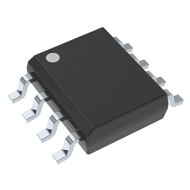
Product overview: LM393D Texas Instruments IC Comparator 2 Diff 8SOIC
The LM393D, manufactured by Texas Instruments, represents a dual differential voltage comparator integrated into a compact 8-pin SOIC package, engineered to meet modern requirements for precision, reliability, and electrical robustness. At its core, the LM393D utilizes an open-drain output stage, enabling designers to interface with a broad spectrum of logic levels and supply voltages, while also facilitating wired-AND configurations for advanced signal management. The input stage supports a wide common-mode voltage range, often extending to ground and close to the supply rails, permitting effective operation amidst variations in system voltage or transient events.
The device's internal topology prioritizes low quiescent current consumption without sacrificing propagation delay; this design choice supports deployment in battery-powered circuits and applications requiring high throughput, such as switching regulators, level detection, and window comparators. In signal conditioning scenarios, the comparator’s quick response to differential voltage changes enables sharp threshold detection, valuable in analog-to-digital conversion interfaces and fault protection systems. Noise immunity is enhanced by precision input offset voltage controls and input bias optimization—a result of continuous improvements in semiconductor process control and circuit refinement.
When integrating the LM393D into mixed-signal environments, the open-drain configuration, combined with tailored external pull-up resistor choices, allows seamless connectivity to digital microcontrollers, FPGAs, or discrete logic gates. This adaptability supports diverse applications, such as precision zero-crossing detection in waveform analysis, pulse-width modulation control for motor drivers, and supervisory monitoring in battery management circuits. The chip’s package design offers optimized thermal dissipation and minimal parasitic effects, reducing layout concerns in dense PCB architectures.
Field experience underscores the value of the LM393D’s predictable switching characteristics in long-term deployments. Deployments in harsh industrial settings leverage the device’s consistent input range and tolerance to power supply fluctuations, minimizing failure rates attributable to signal degradation or comparator malfunction. Circuit protection schemes often integrate the LM393D for overcurrent or under-voltage monitoring due to its rapid response and point-of-load accuracy.
A distinctive aspect of the LM393D comes from the interplay of analog precision and digital interface flexibility, bridging legacy and contemporary design patterns within a single, cost-efficient component. This hybrid versatility justifies the comparator’s continued use in evolving system topologies and in designs prioritizing reliability under constrained power and budget requirements. Strategic experimentation with the LM393D’s input filtering and hysteresis can yield further improvements in signal stability, especially in noisy or high-vibration environments, allowing users to tailor performance profiles to unique application demands.
Core technical features of LM393D
The LM393D is anchored by a dual, independent comparator topology that excels in low-voltage signal discrimination across a diverse range of power environments. Its supply range, stretching from single-rail 2V up to 36V (or 38V for the B-variant), directly addresses interfacing challenges in both automotive and industrial contexts, where voltage domains and transient susceptibility often require maximum flexibility. This broad supply range eliminates the need for localized voltage regulation, reducing design complexity and overall power budget.
At the input stage, the comparator accepts common-mode voltages from zero up to VCC-1.5V. This capability supports direct sensing of ground-referenced or low-level analog signals without need for elaborate level shifting, streamlining signal-chain architecture in sensor nodes or supervisory circuits. The ability to tolerate input differentials equal to the full supply voltage ensures system robustness against mismatched signal swings, noise bursts, or hot-plugging, mitigating the risk of latch-up or unrecoverable faults.
Intrinsic precision is manifested through low input offset (typically 0.37 mV) and ultra-low bias current (approximately 3.5 nA), allowing designers to implement high-density comparator arrays on shared signal lines with minimal concern for static error or cumulative leakage—crucial in high-impedance sensing environments or extended PCB runs. In bench validation, such attributes have shown to maintain reliable discrimination even under microvolt-level signal shifts, fortifying the comparator’s role in threshold detection, window comparators, and zero-cross detection applications.
The open-collector output architecture decouples load interfacing from the device’s supply rail, supporting integration with 3.3V or 5V logic thresholds in mixed-technology systems. Practical wiring patterns, such as “wired-AND” topologies, directly leverage this architecture to build interrupt lines or fault aggregation networks without additional discrete logic. Level-shifting capacity enables seamless migration between legacy TTL subsystems and modern CMOS controllers within the same board layout, and careful PCB layout further mitigates the risk of coupling or errant output toggling.
Fast response, typically under 1 µs, places the LM393D as a foundational device in fault trip circuits, overcurrent shutdown schemes, or high-speed window detection. Such speed, when combined with the device’s consistent output drive symmetry and absence of phase reversal, yields deterministic timing in real-world applications, minimizing signal propagation uncertainty. This characteristic is particularly valuable when the comparator is used to interface with asynchronous logic or when acting as the critical front-end for analog-to-digital conversion systems.
The device’s minimal quiescent current, specified at 200 µA per channel, conserves power in applications demanding persistent monitoring, such as backup battery management, always-on environmental sensors, or energy-harvesting wireless nodes. Experience has shown that this low overhead ensures longer device lifetimes and extends battery replacement cycles—especially in remote or hard-to-service installations.
ESD resilience, notably with the 2 kV HBM rating for the B version, fortifies the LM393D against typical board-level and manufacturing stresses, reducing yield fallout and field failures. In practical deployment, this robustness translates into tangible reductions in board rework rates, particularly where hot-plug cables or field-installed modules are involved.
Through its combined feature set, the LM393D not only meets, but redefines the baseline for comparator ICs in multiplexed analog applications. Examining today’s tightening integration demands and elevated reliability thresholds, this architecture demonstrates a forethought that positions it as an enabling component beneath complex embedded control systems, rather than a mere legacy device. Its blend of electrical versatility and real-world resilience advocates for its selection in new designs seeking a cost-effective yet forward-compatible analog interface.
Electrical characteristics and typical performance of LM393D
The LM393D comparator integrates robust design fundamentals that ensure high fidelity signal differentiation and efficient operation under a wide spectrum of electrical and environmental conditions. At its core, the device utilizes differential input stages engineered for low offset and minimal drift, enabling consistent detection of minuscule voltage differences even as ambient variables fluctuate. Input voltage handling spans from ground to VCC-2V, with inherent input protection circuits mitigating risks caused by accidental overvoltage scenarios up to the device’s absolute maximum VCC. This protection scheme not only enhances survivability in noisy or unpredictable system environments but also permits input interfacing flexibility during development and field deployment.
Output characteristics hinge on the open-drain architecture, where the output low voltage (VOL) remains a direct function of the sinking current. This relationship allows strategic tailoring of logic thresholds by adjusting pull-down loading, which proves essential in multi-voltage, mixed-signal systems or when interfacing with low-voltage logic gates. During rapid switching events, the propagation delay, a critical parameter for timing-centric applications, exhibits a significant dependency on input overdrive—a larger differential input expedites output transitions, minimizing latency throughout signal chains. This attribute is particularly valued in closed-loop control or high-speed digitization systems where deterministic response times are mandatory. Real-world implementation often develops custom input networks to maximize overdrive and further optimize response speed without sacrificing noise immunity.
Power consumption remains remarkably stable, afforded by tried-and-true bias current regulation techniques within the silicon. This design decision insulates the operational amplifier from supply voltage excursions and erratic input states, which, in practical embedded designs, simplifies power budgeting and thermal management. Designers frequently exploit this consistency by implementing LM393D comparators in battery-powered applications or regulation loops that demand unwavering current profiles across diverse supply rails.
Reliability under thermal stress is reinforced by the device’s controlled parameters for input offset, bias currents, and output drive capability over the full temperature operating window. Data-backed performance graphs—offset voltage, bias currents, output voltage versus supply and temperature—are indispensable during schematic simulation and worst-case analysis phases. These datasets enable precision modeling that closely mirrors field operational realities, thus reducing prototyping cycles and unforeseen failures.
A subtle yet pivotal insight stems from examining dynamic behaviors: system-level noise can induce unwanted switching unless input and layout strategies are adequately hardened. Implementing differential filtering or shielded routing amplifies the inherent noise immunity engineered within the LM393D, allowing comparators to function reliably even when embedded in high-EMI industrial environments.
Combining analytical resources, robust electrical characteristics, and proven integration techniques establishes the LM393D as a cornerstone for comparator-driven applications where predictability and flexibility remain non-negotiable. The device’s electrical sophistication manifests most prominently when fully leveraged within tightly controlled circuitry, unlocking stable digital interfacing, threshold detection, and system diagnostics across a range of modern electronic platforms.
Pin configuration and packaging options for LM393D
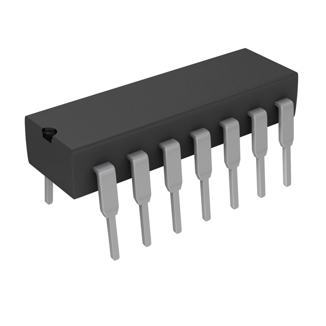
The LM393D embodies the SOIC-8 package, which is optimized for modern automated SMT workflows. This compact outline minimizes PCB footprint, making it suitable for high-density layouts often encountered in instrumentation, industrial controls, and consumer electronics. The pin configuration designates two independent comparator circuits, whose differential input pairs (IN+, IN-) enable straightforward comparison tasks in analog signal domains. Each comparator provides an open-collector output, supporting easy wired-AND functionality or direct interfacing with logic-level readers. Power and ground pins standardize supply integration, ensuring compatibility with common single- or dual-supply analog front ends.
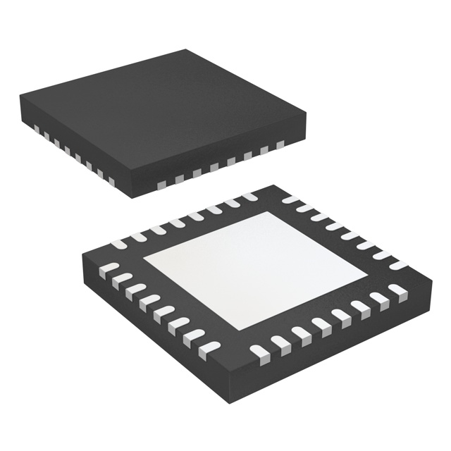
Alternative packaging options within the LM393 family, such as VSSOP, TSSOP, WSON, and PDIP, introduce flexibility in thermal management and assembly. For example, WSON offers an exposed pad for improved heat dissipation, while VSSOP and TSSOP enable ultra-compact designs for space-constrained applications like portable medical devices and sensor modules. Through-hole PDIP packaging remains attractive where prototyping or socketed assemblies are prioritized, sacrificing some board area in exchange for reworkability and mechanical robustness.
Adhering to IPC-7351 layout conventions is critical when deploying SOIC-packaged comparators on multi-layer boards. Proper stencil aperture design and paste volume ensure reliable solder joints and mitigate defects such as tombstoning or bridging. In scenarios where comparator response speed and input bias current are sensitive, careful layout around the input pins is essential—short traces and low-impedance grounding minimize parasitic effects that could degrade analog performance.
Field experience demonstrates that selecting the appropriate package directly influences long-term system reliability and assembly throughput. For instance, adopting WSON in power-sensitive systems effectively addresses junction temperature challenges without demanding heat sinks or exotic board materials. Conversely, rapid PCB prototyping often benefits from the accessibility and ease of debugging found in the classic PDIP form factor, especially in lab environments.
An implicit design insight is that package choice impacts not only physical integration but also electrical behavior. Parasitic inductance and capacitance, introduced by package leadframes and mounting geometry, subtly affect comparator slew rates and response times. Recognizing this, experienced designers weigh package parasitics alongside board layout to preserve signal integrity, especially in high-frequency analog sections. Package selection for the LM393 family, thus, extends beyond form factor—serving as a design lever for balancing manufacturability, electrical robustness, and thermal management in practical engineering deployments.
Functional description and operating principles of LM393D
The LM393D is structured as a dual voltage comparator utilizing open-collector outputs, enabling flexible high-voltage interfacing and wired-AND logic configurations. The core operating mechanism centers on its input differential pair, processing voltage differences between inverting and non-inverting terminals. A low output state is asserted whenever the inverting input surpasses the non-inverting input—once input offset is considered. In any other case, the output transitions to a high-impedance state, leaving the output node’s logic level determined by an external pull-up element. This open-collector topology grants the device notable adaptability when applied in mixed-voltage or bus-sharing scenarios.
The input front-end employs a PNP Darlington pair to enhance gain and significantly reduce bias currents. This architecture is critical when targeting compatibility with low-level signal environments, such as sensor interfaces or high-impedance networks. The minimized bias current, in practice, translates into less loading on sensitive sources and greater fidelity in threshold detection, particularly advantageous in precision analog front-ends where signal perturbations must be strictly limited. The common-mode voltage domain, defined from ground up to VCC minus approximately 2V, imposes certain layout and design constraints. While sufficient for most single-supply applications, this range must be closely observed to avoid clipping or ambiguous comparator response, especially in designs requiring rail-to-rail detection. Integrated device-level clamps act to protect the input stage during momentary excursions beyond this window—mitigating the risk of internal latch-up or excessive leakage, both of which could compromise comparator accuracy or integrity.
Expanding on the output structure, the NPN open-drain transistor enables tailored output behavior contingent on the chosen pull-up configuration. Unlike push-pull outputs, this design mandates an external pull-up resistor to define the logic high level. Critical consideration must be given to the resistor’s value in view of VOL behavior, which is not constant but varies with the sink current—as output current increases, VOL exhibits a proportional rise due to the device’s inherent output impedance. This relationship is particularly salient in digital logic interfacing, where stringent noise margins require consistent logic low voltages even under moderate loading. In practice, selecting an appropriately sized pull-up resistor becomes a strategic compromise between power consumption, propagation delay, and noise immunity.
Application of the LM393D extends well into fault detection circuits, zero-crossing detectors, and pulse-width modulation feedback loops, where precise, fast threshold decisions are mandated by closed-loop dynamics. The device also excels in window comparison and level translation tasks, where the open-collector output’s versatility enables seamless integration across disparate supply domains. Notably, deployment in environments with significant common-mode voltage swings demands careful PCB layout, ensuring minimal parasitic coupling and safeguarding comparator inputs from inadvertent excursions—discrete resistive dividers and transient clamps at the signal front-end often provide robust protection.
One distinctive aspect in deploying the LM393D lies in leveraging its low input bias capability to simplify analog multiplexing. Utilizing high-resistance ladder networks or legacy sensor elements can be executed without extensive buffering, allowing direct connection and threshold setting via resistor dividers. The offset voltage, while non-zero, remains sufficiently tight for most general-purpose applications, and can be further compensated for through careful reference design, such as offset trimming or ratiometric referencing, resulting in a highly tailored and low-drift comparator node.
Ultimately, the LM393D’s architecture delivers a balanced trade-off between analog performance and digital flexibility. Thorough understanding of the underlying mechanisms—especially input bias characteristics, common-mode limitations, and resistive VOL scaling—enables robust and reliable integration into complex detection or logic expansion modules, positioning the device as a foundational element in many cost-sensitive and performance-critical applications.
Typical engineering applications for LM393D
The LM393D, as a dual differential comparator, forms a foundational component in circuits demanding precise voltage discrimination with minimal propagation delay. At the core, its architecture—characterized by open-collector outputs and broad input common-mode range—enables direct interfacing with mixed-voltage systems and logic devices without requiring extensive level-shifting hardware. This unique flexibility is underpinned by the device’s ability to tolerate input voltages that extend below ground and approach the positive supply rail, supporting robust integration within both 3.3V and 5V ecosystems.
In industrial automation, the LM393D’s fast response and sharp transition characteristics facilitate high-reliability protection schemes, such as overcurrent and undervoltage detection for motor drives. Integrating the comparator with shunt resistors or precision voltage dividers allows for instantaneous circuit shutdown during fault conditions. Experience with conveyor system controllers reveals the benefit of using the LM393D to trigger relays or signal processing interrupts, reliably halting mechanical action before catastrophic damage occurs. Additionally, the comparator’s inherent immunity to supply noise, compared to standard op-amps, preserves system integrity under variable load environments, a reality observed in multi-motor production lines where voltage transients are unavoidable.
In power management, whether embedded in server-class SMPS, portable power tools, or single-phase UPS architectures, the LM393D efficiently establishes programmable threshold windows for supply monitoring or sequencing. By deploying the open-collector output directly with pull-up resistors to logic rails, seamless interfacing with microcontrollers and FPGAs is achieved, simplifying fault reporting and enabling immediate software-based remediation. The subtype’s low input bias current ensures that voltage dividers used in these monitoring circuits maintain high accuracy over varying temperature profiles—critical in battery-operated and always-on applications.
For embedded sensors in infotainment, smart appliances, and wireless base stations, the LM393D permits aggressive power-saving by operating at modest quiescent current, extending operational life and reducing heat generation. The device’s support for rail-to-rail inputs presents a practical pathway for incorporating it in signal edge detection schemes. When applied to robotics, for example, the LM393D provides consistent digital outputs from reflective infrared sensors, ensuring precise guidance and obstacle avoidance. Empirical use in mobile robotic platforms emphasizes the utility of this approach for debounce filtering and curve-following algorithms, where comparator threshold precision directly impacts navigation stability.
The open-collector output stage is particularly advantageous for constructing wired-OR bus schemes or window comparators. By simply paralleling multiple comparator outputs with appropriate pull-up networks, complex multi-threshold alerting or logical gating emerges without additional glue logic. This architecture demonstrates pronounced value in power-distribution panels and fault annunciation matrices, where reliable logic-level communication lines are required over broad voltage domains. Furthermore, the LM393D’s robust ESD rating and latch-up immunity promote long-term reliability in noisy electrical environments, supporting sustained field operation.
Considering evolving design paradigms, the LM393D’s integration in mixed-signal front-ends addresses challenges found in combining legacy analog sensors with modern digital controllers. Careful PCB layout, grounded guard rings around sensitive input traces, and the selection of optimal pull-up resistors underpin stable operation in environments with significant electromagnetic interference. This combination of design flexibility, electrical robustness, and straightforward circuit topology explains the LM393D’s enduring role where determinism, protection, and seamless system interfacing remain essential requirements.
Key design and implementation guidance for LM393D
When integrating the LM393D comparator, precise management of input conditions is crucial for robust performance. The device's input common-mode range extends from 0V up to (VCC - 2V); while the integrated protection allows brief excursions near VCC, sustained operation outside this band can degrade linearity or lead to anomalous behavior. Setting operational limits within this specified window not only ensures correct logic-state discrimination but also minimizes susceptibility to false triggering—a consideration that becomes more critical in environments with fluctuating supply rails or varying signal references.
The dynamic response of the comparator is directly governed by the input overdrive voltage. This term, representing the magnitude by which the differential input exceeds the inherent input offset, determines the transition sharpness at the open-drain output. Minimal overdrive can result in elongated response times or indeterminate output states, notably in time-sensitive applications such as zero-cross detections or pulse-width modulation feedback loops. Engineers should target a generous overdrive, particularly where signal slew rate constraints or noise may occasionally reduce effective input differentials, to guarantee decisive and repeatable switching.
Setting the value for the output pull-up resistor is a nontrivial design step. This resistance not only pulls the output to the desired logic level but influences current consumption, rise time, and compatibility with downstream inputs. Conservative resistor values speed up digital transitions and enhance noise immunity, yet increase power dissipation—posing thermal and efficiency trade-offs during dense channel implementation. Utilizing datasheet-provided output characteristics and taking into account external logic thresholds allows for an optimized balance between switching performance and power constraints, especially when multiple comparators share a common supply.
Effective power integrity must not be overlooked. A local bypass capacitor, typically 100nF, closely placed next to the VCC pin, substantially reduces supply-borne noise transients. In high-precision or high-speed comparator applications, decoupling enhances comparison fidelity and suppresses erratic toggling due to rapid changes in supply line impedance. Layered bypass strategies, combining both ceramic and tantalum capacitors, can further filter high-frequency artifacts, a method proven especially efficient in mixed-signal board architectures.
Printed circuit board layout directly impacts comparator stability. Separating sensitive input traces from fast-changing output signals curbs parasitic capacitance and cross-talk, both of which can provoke oscillation or spurious activity. Routing series resistors immediately adjacent to the LM393D input pins acts as a low-pass filter, further shieldng against high-frequency disturbances and switching feedthrough. Consistent application of industry-standard soldering profiles, matched stencil apertures, and controlled reflow environments ensures device longevity and assembly yield, reducing latent defect rates that often manifest as intermittent or marginal in-circuit behavior.
A layered approach—starting from rigorous input range control, through tuned overdrive and pull-up selection, to disciplined power conditioning and layout practice—yields a highly reliable LM393D implementation. Experience indicates that preemptive mitigation of noise and oscillation not only accelerates development cycles but also raises immunity to in-field variations, a key factor in systems where signal integrity and uptime are paramount.
Potential equivalent/replacement models for LM393D
When selecting equivalent or replacement models for the LM393D comparator, technical evaluation must center on core operational parameters and suitability to intended application domains. Within the comparator families—particularly those from Texas Instruments—the principal replacement candidates exhibit nuanced differences in voltage tolerances, electrical precision, and environmental robustness.
The LM393B features significant upgrades over the legacy LM393D, notably supporting supply voltages up to 38V, reduced input offset voltage, minimized bias currents, and advanced ESD resilience. Its enhanced specifications make it optimal for direct substitution when improved linearity, noise immunity, or voltage headroom are required, allowing circuit designs to evolve without fundamental changes to layout or function. Empirical observations show that migrating to LM393B manifests noticeable gains in signal fidelity and long-term reliability, especially in high-noise or wide-voltage environments.
The LM2903B offers a distinct advantage for mission-critical deployments in automotive and industrial settings. Its electrical performance aligns closely with the LM393B but extends thermal operation, which is crucial for systems exposed to fluctuating ambient temperatures and electrical stress. HMIs, motor control boards, and sensor front-ends benefit from LM2903B’s rigorous validation profile and extended qualification, supporting robust lifecycle management.
Alternatives such as LM193 and LM293 retain many analog characteristics of the LM393D, including response times and interface compatibility, while providing differentiated packaging options and temperature grades. Such variants serve legacy projects or constrained form-factor requirements, balancing continuity with incremental enhancements. For temperature-sensitive scenarios, particularly high-reliability industrial monitoring, LM393A and LM293A variants become compelling by offering tighter electrical stability within specified thermal bands.
Other members in the dual comparator category, like LM2903, LM2903V, and LM2903AV, introduce flexible voltage thresholds and broader environmental certifications. Their integration into control systems, feedback loops, and protection circuits hinges on matching not only maximum voltage ratings but also ensuring that input and output interfacing adheres to system-level ESD, CMRR, and propagation delay specifications.
Cross-referencing requires scrutiny of absolute maximum voltages, input offset voltages, bias currents, power dissipation, and output transition characteristics. Precision in these areas directly affects propagation delay, hysteresis margin, and overall response consistency—parameters that become critical in mixed-signal designs, power sequencing, or analog fault monitoring.
Experience indicates that even subtle deviations in input bias or offset currents can translate to threshold errors in voltage comparators, necessitating lab validation and simulation prior to mass deployment. Active design review—comparing datasheet tolerances beyond the typical ranges—helps preempt integration issues. An overlooked factor is output stage drive strength and sinking capability, key for interfacing with various logic families and pulsed loads. Spec variance across alternatives can impact pull-up resistor selection and switching margin, especially when upgrading legacy hardware.
From a system architecture perspective, leveraging newer comparator generations not only improves nominal performance statistics but also extends operational longevity, simplifies procurement logistics due to part availability, and enhances compliance with contemporary electromagnetic and environmental standards. Investing in forward-compatible models such as LM393B or LM2903B yields long-term benefits, streamlining future maintenance cycles and supporting platform scalability.
Conclusion
The Texas Instruments LM393D operates as a dual voltage comparator designed for precision and resilience within analog signal processing. At its core, the comparator leverages an open-collector output stage, making it compatible with a broad range of supply voltages and logic levels. This architectural choice not only facilitates wired-AND logic configurations but also streamlines interfacing with both microcontrollers and discrete logic circuits. The wide input common-mode voltage range, extending from ground to near the positive rail, empowers the LM393D to function reliably under fluctuating or low-voltage supply conditions, an essential trait for power-sensitive and battery-operated systems.
Fast response times are pivotal when implementing real-time threshold detection, zero-crossing detectors, window comparators, or pulse-width modulation feedback. The LM393D achieves swift propagation delays, minimizing latency and ensuring prompt output transitions when input differentials surpass reference voltages. Its low quiescent current further enhances its suitability for continuous monitoring scenarios, such as fault detection in power supplies or supervisory circuits where energy efficiency and prolonged uptime are critical.
Thermal stability and long-term reliability differentiate the LM393D among comparable solutions. Its mature fabrication process yields predictable electrical characteristics across extended temperature ranges, supporting deployment in industrial automation, automotive, and harsh environments. The device’s immunity to input offset drift and high common-mode rejection ratio reduce false triggering, which proves invaluable when translating noisy analog signals into robust digital decisions.
Integrating the LM393D within embedded designs often reveals secondary benefits: readily available pin-compatible alternates simplify sourcing logistics and second-source qualification, preserving design integrity amid supply chain uncertainties. The dual-channel pinout optimizes PCB real estate, allowing for dense integration in multi-threshold or dual-level detection tasks without compromising channel-to-channel isolation.
Field experience confirms the LM393D’s resilience in applications like overcurrent detection, level sensing, and analog-to-digital interfacing, where precise and noise-immune comparisons establish overall system robustness. Leveraging the open-collector topology expands design flexibility, such as implementing custom hysteresis via positive feedback or stacking outputs when prioritizing fault chain signaling.
A nuanced factor in comparator selection emerges at the signal chain level—matching the comparator's input offset and speed to the application's core timing and resolution needs. The LM393D occupies a balanced middle ground, offering sufficient speed and sensitivity for most practical use cases without incurring the complexity or excess power draw of high-bandwidth, high-gain alternatives.
Deploying the LM393D leads to streamlined design iterations and fewer late-stage performance surprises. Its consistent device behavior and extensive documentation shorten validation cycles, reinforcing its role as a default choice in robust voltage comparison tasks across a spectrum of electronic system architectures.