>
>


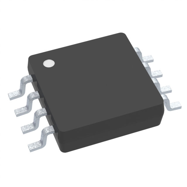
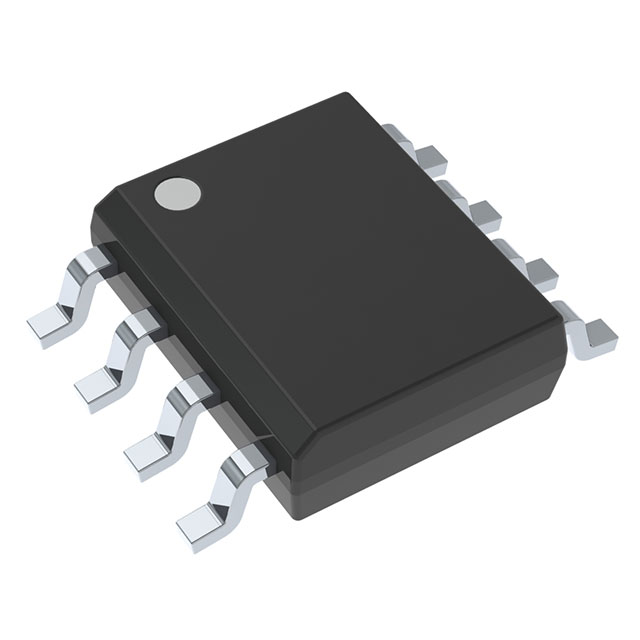
LM358MX Product Overview
The Texas Instruments LM358MX represents a benchmark in dual operational amplifier (op-amp) design for space-constrained analog systems. Incorporating two independent, internally frequency-compensated op-amps within an 8-pin SOIC, the LM358MX focuses on achieving balance between integration density, electrical performance, and design flexibility. Its architecture supports single or dual supply operation, enhancing circuit simplicity for mixed-voltage environments without requiring complex level-shifting or extensive biasing networks. This feature, combined with rail-to-rail input/output characteristics, allows the amplifier to maintain signal integrity even in low-supply, low-headroom applications.
Core to the LM358MX’s utility is its immunity to latch-up and its stable performance across a broad temperature range, supporting reliability-critical deployments. The input common-mode range includes the negative rail, a characteristic that simplifies single-supply designs by expanding the possible signal domain and eliminating the need for dual-rail biasing in many applications. Input offset voltage and bias current remain within typical tight tolerances that are sufficient for most filtering, buffering, and signal conditioning stages in instrumentation, sensor interfaces, and feedback control loops.
The benefits become particularly evident in high-density PCB layouts where real estate and crosstalk limitations drive package selection. The SMD SOIC-8 profile ensures mechanical stability under automated assembly processes, contributing to long-term system robustness in environments subject to vibration or thermal cycling. Layout experience shows that placing decoupling capacitors close to the supply pins further enhances low-noise performance, especially in sensitive analog front-ends. Moreover, the generous gain-bandwidth product supports both DC and moderately fast AC applications, from low-frequency amplifiers to moderate-speed active filters. While not designed for high-speed scenarios, in practical audio preamps, sensor signal conditioners, or low-frequency analog computing circuits, the LM358MX avoids the pitfalls of instability or high power consumption often associated with faster amplifiers.
From a cost-to-performance perspective, the LM358MX enables rapid prototyping with predictable results, reducing validation cycles during iterative development. Its pin-compatible footprint with other popular op-amps supports late-stage design modifications and circuit scaling without substantial rework, an attribute that enhances lifecycle management in evolving product lines. Subtle design decisions—such as integrating ESD protection diodes and optimizing quiescent current—translate to minimized failure rates in deployed field applications where maintenance access is constrained.
A thoughtful selection of external passive components, tailored to the op-amp’s input characteristics, further refines the system’s noise floor and frequency response, yielding reliable, high-SNR analog sections in both consumer and industrial devices. By leveraging the LM358MX’s balance of efficiency, stability, and versatility, complex multi-channel analog applications can be efficiently architected, reflecting a mature convergence of electrical, mechanical, and cost optimization disciplines.
Key Features and Functional Specifications of LM358MX
The LM358MX operational amplifier distinguishes itself as a multi-purpose analog building block, emphasizing adaptability and robustness at the circuit level. The integration of two independent, high-gain op-amps within a single 8-SOIC package offers immediate benefits for space-constrained designs, directly targeting the needs of modern surface-mount assemblies. Each amplifier is optimized for low-power operation, allowing deployment in both battery-powered and line-powered systems. The architecture supports a wide supply voltage range, typically from 3V to 32V for single supply or ±1.5V to ±16V for dual supplies, accommodating both legacy and advanced analog interfaces with minimal reconfiguration.
Analyzing its input/output characteristics, the LM358MX incorporates differential input stages with a common-mode range that extends to ground on a single supply. This input structure enhances design flexibility in applications where low-side sensing or ground-referenced signals are prevalent. Output stages are tailored to sink and source moderate currents while maintaining stability across variations in load capacitance and supply voltage. Such predictable behavior streamlines the signal chain, mitigating issues related to latch-up or oscillation, which are common in less robust op-amp topologies.
From an engineering perspective, the LM358MX’s general-purpose nature is evident in its application breadth. In amplification roles, the device consistently delivers linear gain performance for sensor interface, audio buffering, or active filtering, even under supply fluctuations or varied input levels. The ability to implement filtering, summing, or basic analog computational functions using industry-standard feedback techniques further reinforces its utility as a design cornerstone. Its low quiescent current—typically around 0.5 mA per channel—directly contributes to reduced thermal load, prolonging component lifespan in densely-packed PCBs.
The package format—8-SOIC—optimizes board real estate without sacrificing accessibility for automated assembly processes such as pick-and-place and reflow soldering. Moreover, the mature process technology underlying the LM358MX has undergone extensive field validation, minimizing concerns related to long-term drift, offset voltage instability, or performance degradation under harsh environmental cycling. This stability is a strong factor in its preference for instrumentation, industrial control, and consumer electronic subsystems, where reliable, repeatable analog performance underpins system-level functionality.
In practical deployment, the LM358MX offers several integration conveniences. For example, the wide input voltage tolerance simplifies the interface with microcontrollers and analog-to-digital converters across disparate reference domains. Designers implementing analog signal chains often leverage the device’s immunity to phase reversal and tolerance to capacitive loading as a safeguard against unanticipated board-level anomalies, minimizing debug cycles and field failures.
The strategic value of the LM358MX emerges not only through its feature set, but also through its mature supply chain and interchangeability with other op-amp families, enabling streamlined qualification and lower bill-of-materials complexity. Forward-looking designs continue to capitalize on these traits, recognizing that robust analog infrastructure anchors rapid prototyping and accelerates product iteration cycles without compromising on reliability.
Typical Applications and Engineering Considerations for LM358MX
The LM358MX operational amplifier, built on a robust bipolar process, exhibits a versatile dual-channel configuration, facilitating streamlined circuit design across sensor interfaces, signal conditioning modules, switched-capacitor filters, and basic waveform generators. Its rail-to-rail output behavior, while not absolute, enables consistent linear swing in low-voltage applications, which aligns well with microcontroller-based data acquisition systems and compact industrial measurement nodes. Critically, the reduced form factor afforded by the tightly integrated dual op-amp minimizes routing complexity and PCB footprint, fostering higher channel density and modular expansion in both prototyping and production environments.
Diving into key engineering parameters, input offset voltage and bias current command particular attention, especially in precision sensor front-ends or transducer preamps where microvolt-level signal integrity is non-negotiable. The LM358MX typically presents an input offset voltage in the millivolt range, compatible with most low- to mid-precision circuits, though offset trimming or dedicated calibration may be required for ultra-high accuracy scenarios. The unit’s moderate gain-bandwidth product, typically around 1 MHz, matches typical requirements for slow-to-moderate speed analog front-ends: auto-zero amplifiers or higher-spec unity gain op-amps would be selected for more demanding dynamic applications.
Power management further distinguishes the LM358MX in battery-centric systems and distributed sensor arrays. Its low quiescent current profile—often under 1 mA per channel—enables deployment in energy-constrained environments without frequent maintenance or excessive thermal buildup. In practice, stable operation is achieved with minimal supply decoupling, though incorporating local 100 nF to 1 μF ceramic capacitors adjacent to the supply pins yields optimal dynamic response during transients or in noisy digital systems. Efficient layout, with ground planes and short trace lengths, directly augments resilience against electromagnetic interference.
The SOIC packaging blends mechanical resilience with reflow solder compatibility, allowing seamless surface-mount assembly and automated test coverage. In high-throughput manufacturing, process stability is maintained under the JEDEC moisture sensitivity classification, minimizing field returns attributable to solder joint fatigue or package delamination.
It is often underestimated how the LM358MX, owing to its legacy topology and universally supported pinout, simplifies multi-vendor sourcing—enabling cost optimization and contingency planning without major redesign effort. Real-world deployments highlight this practical edge, as the BOM flexibility allows rapid design iterations and supply chain remapping in response to volume shifts or logistics disruptions. Ultimately, the LM358MX’s mature feature set and predictable characteristics underpin reliable analog subsystems in diverse sectors—from remote environmental logging to low-cost consumer motor controllers—illustrating how a balanced design approach yields enduring utility across generations of analog designs.
Environmental Compliance and Regulatory Status of LM358MX
Environmental compliance remains a pivotal consideration in the qualification process of integrated circuits for international markets. The LM358MX demonstrates adherence to stringent regulatory standards, which directly impacts its suitability for deployment in a wide range of environmental policy frameworks.
At the core, RoHS3 compliance establishes the device is manufactured without the use of hazardous substances specified in the directive, such as lead, cadmium, hexavalent chromium, and select brominated flame retardants. This level of compliance is critical in minimizing the ecological footprint of electronic assemblies, ensuring the component can be seamlessly designed into consumer electronics, industrial controls, and medical equipment distributed across jurisdictions with varying environmental legislation. The regulatory scope extends beyond product design, influencing procurement choices, material declarations, and lifecycle analysis in downstream applications.
The component’s status as REACH unaffected indicates the absence of Substances of Very High Concern (SVHCs), simplifying material compliance documentation for OEMs and contract manufacturers. This feature reduces administrative overhead and accelerates regulatory due diligence during the product approval cycles. In practical terms, it streamlines the bill of materials (BOM) management and supports risk mitigation strategies for companies seeking to avoid costly supply chain disruptions due to chemical non-conformance.
Trade classification contributes an additional operational advantage: the LM358MX is categorized under ECCN EAR99 and the Harmonized Tariff Schedule (HTS) code 8542.33.0001. EAR99 classification confirms the device does not require specific export licenses for most destinations, except for embargoed or restricted countries. The specific HTS code facilitates accurate tariff calculation and customs clearance, providing predictability in international logistics and lowering the potential for border delays. This regulatory clarity benefits not only compliance teams but also logistics, planning, and sourcing functions, reinforcing supply chain agility.
Integrating the LM358MX into global product designs becomes a low-risk choice due to its robust regulatory profile. Complexities in cross-border transfer, component traceability, and EHS (Environment, Health, and Safety) reporting are minimized. This not only accelerates new product introduction (NPI) schedules but also supports long-term maintainability of product lines as environmental regulations evolve. A notable insight emerges when considering growing global focus on extended producer responsibility and circular economy models: components like the LM358MX act as enablers for regulatory resilience, future-proofing designs against tightening compliance thresholds.
In summary, the LM358MX’s comprehensive compliance certification fosters market access, reduces operational friction, and empowers design teams to deliver compliant products with lower regulatory risk exposure. Its environmental and trade status form the foundation of its appeal for projects demanding global compatibility and sustained regulatory assurance.
Potential Equivalent/Replacement Models for LM358MX
The process of selecting suitable equivalents or replacements for the LM358MX operational amplifier involves a multi-layered evaluation that begins with core device architecture and extends to system-level integration. The LM358MX, a widely adopted dual op-amp, is implemented across numerous analog signal conditioning tasks owing to its balanced performance and availability in compact SMD packages. Engineers addressing supply chain volatility or project updates prioritize maintaining functional continuity and minimizing disruption during substitution.
At the device level, a focus on critical electrical parameters—such as input offset voltage, slew rate, unity-gain bandwidth, and supply voltage range—forms the foundation for a sound equivalency assessment. For instance, the Texas Instruments LM358 family delivers line-by-line compatibility, offering identical electrical characteristics across multiple package types, including SOP and TSSOP, thus streamlining the replacement process in existing PCBs. Similarly, the STMicroelectronics LM358N stands out for through-hole deployment, retaining the same internal topology and guaranteeing predictable bias currents and input characteristics.
When designs transition between different package types or manufacturing processes, options such as ON Semiconductor’s LM358DR2G provide versatile SMD compatibility and maintain parametric consistency, lending flexibility to automated assembly lines. Where application environments impose a demand for broader supply voltages or enhanced robustness, the MC1458 from ON Semiconductor (formerly Fairchild) presents a strategic advantage, enabling wider operational headroom without necessitating substantial circuit modifications.
Thorough pinout matching is non-negotiable; even minor differences can lead to malfunction or reduced lifecycle reliability. Structured evaluation using datasheet cross-referencing and simulation validates drop-in compatibility, preempting shifts in common-mode range or changes in noise performance that could affect precise analog systems. Signal chain impact is often more pronounced in high-gain or bandwidth-sensitive applications, underscoring the necessity for oscilloscope verification and prototype-based validation.
Application scenarios influence selection criteria. In compact sensor conditioning modules, size and power consumption take precedence, favoring equivalent devices with low quiescent current and matched surface-mount footprints. Conversely, in industrial control units where component resilience and long-term supply assurance are critical, established multi-vendor manufacturing lines—such as those supporting standard LM358 variants—demonstrate tangible benefits in risk mitigation.
Beyond datasheet parameters, real-world implementation often uncovers differences in EMI immunity or temperature drift, which can be critical in automotive or instrumentation environments. Incremental bench testing under representative operating conditions reveals nuanced aspects of device behavior, shaping best practices in model selection. Design teams frequently leverage engineering change notice (ECN) processes to document and communicate equivalence assessments, ensuring traceability and regulatory compliance.
The ongoing consolidation within the analog IC industry introduces further complexity. The rising prevalence of pin-to-pin compatible drop-ins from second-source suppliers provides valuable flexibility, yet cross-vendor verification remains essential to avoid edge-case discrepancies. Experience demonstrates that supply chain agility and informed cross-referencing contribute as much to successful substitution as technical datasheet matching.
Ultimately, high-fidelity equivalent model selection for the LM358MX requires integrating rigorous specification analysis, hands-on validation, and a proactive supply chain strategy. This layered, evidence-driven approach minimizes risk, ensures stable system performance, and supports resilient product life cycles in dynamic electronic ecosystems.
Conclusion
The LM358MX from Texas Instruments represents a well-engineered analog signal processing solution, integrating dual operational amplifiers within a space-efficient SOIC package. At its core, the device leverages a robust architecture built to operate efficiently across a wide voltage range, supporting both single- and split-supply designs. Its internal structure prioritizes low power consumption while maintaining stable performance, making it suitable for both battery-powered and line-powered systems. The input common-mode range includes ground, enhancing its versatility in single-supply applications—an architectural characteristic that often streamlines circuit design, particularly when precision at low signal levels is critical.
The LM358MX demonstrates consistent performance across temperature and supply variations, underpinned by Texas Instruments’ tightly controlled manufacturing processes and thorough product validation. This ensures predictable behavior and simplifies the process of qualifying circuits in applications where repeatability is key, such as sensor amplification, buffering, and signal conditioning in industrial control systems. The device’s compliance with recognized industry standards, including RoHS and hazard-free certifications, aligns it with the requirements of stringent regulatory environments, ensuring smoother approval cycles during product development.
Application flexibility is further enhanced by the LM358MX's ability to drive moderate capacitive loads without oscillation issues, a recurring concern during circuit prototyping phases. Its rich portfolio of reference designs and application notes accelerates the design cycle, offering proven starting points directly translatable to a variety of contexts, from automotive instrumentation to consumer device interfaces. Engineers frequently exploit the inherent trade-off between bandwidth and quiescent current, balancing power and speed to optimize system performance while adhering to tight budgets and supply chain constraints.
A subtle but important insight emerges from extended practical deployment: reliance on the LM358MX fosters supply chain stability. Its longstanding market presence and multi-vendor support minimize sourcing risks, an increasingly nontrivial factor as component lead times and global availability fluctuate. Furthermore, board-level evaluations often reveal that its tolerance to PCB layout variabilities reduces re-spin occurrences, underlining its forgiving nature in high-mix prototyping environments and real-world deployments. Thus, the chip remains a strategic asset, enabling agile development and reliable scaling from prototype to volume production without introducing unnecessary integration risk.