 >
>


Texas Instruments ESDS312DBVR Product Overview
Texas Instruments ESDS312DBVR is a unidirectional TVS diode array built for board-level protection of high-speed signal interfaces exposed to ESD and transient surge events. Within the ESDS31x family, it targets a common design problem: protecting externally accessible lines without degrading signal integrity or consuming excessive PCB area. Its positioning is especially relevant for Ethernet, USB, and other compact interface implementations where connector-side exposure, dense routing, and compliance margins must all be managed at the same time.
The device integrates two protection channels in a SOT-23-5 package. That combination matters more than it first appears. In many interface designs, the protection element is not evaluated only by its headline clamping rating, but by how efficiently it fits into the routing topology. A two-channel array in a small package can simplify placement near the connector, reduce stub length, and make return-path control easier. In practice, these layout effects often determine whether the protection network performs close to the datasheet level or becomes a source of signal distortion and residual overstress.
At the electrical level, ESDS312DBVR is designed to shunt transient energy away from sensitive downstream circuitry during fast overvoltage events. Under normal operating conditions, it presents low leakage current and relatively low capacitance to the protected line, so it remains electrically quiet. When an ESD or surge event arrives, the junction transitions rapidly into conduction and diverts current to the reference rail before the protected IC input sees destructive voltage. This operating principle is standard for TVS structures, but the engineering value lies in how well the device balances three competing constraints: fast turn-on, low parasitics, and meaningful surge-handling capability.
Texas Instruments specifies IEC 61000-4-2 protection up to ±30 kV for both contact and air discharge. That level is significant for equipment with user-accessible connectors, especially in field environments where cable insertion, unplug events, and electrostatic charge accumulation are routine. In real designs, high IEC ratings provide more than just marketing headroom. They widen the margin against layout imperfections, connector variability, and enclosure-level coupling paths that are difficult to model perfectly during early design stages. A protection device with stronger IEC capability often reduces the need for repeated redesign around marginal compliance failures.
The 25 A surge rating with an 8/20 μs waveform extends its relevance beyond pure ESD events. ESD is extremely fast and high in peak voltage, while surge pulses carry more energy over a longer interval. Supporting both types of stress makes ESDS312DBVR suitable for interfaces connected to longer cables, industrial wiring environments, and networking ports where inductive coupling and transient overvoltage are credible risks. This is an important distinction, because many low-capacitance protection components perform well on ESD but become less convincing once surge robustness is added to the selection criteria.
Its typical line capacitance of 4.5 pF per channel places it in a useful middle ground. It is low enough for many high-speed data interfaces, yet not so aggressively minimized that surge capability becomes trivial. This tradeoff deserves careful attention. Very low capacitance is often treated as the primary metric for signal-line protection, but that view is incomplete. In practical interface protection, capacitance must be evaluated together with clamping behavior, package inductance, leakage, and the actual frequency content of the signal. A device with slightly higher capacitance but stronger clamping stability and better transient current handling can be the better system choice, particularly when the channel budget can tolerate a few picofarads.
For Ethernet and USB-related use cases, this balance is often appropriate. Ethernet lines, especially in cost-sensitive or space-constrained equipment, need protection that does not excessively load the differential path or distort common-mode behavior. USB designs similarly require low enough parasitics to preserve eye integrity while maintaining resilience against connector-originated ESD strikes. In both cases, the protection device should be viewed as part of the channel, not as an isolated reliability accessory. That perspective usually leads to better component selection and fewer late-stage signal integrity surprises.
The unidirectional architecture also shapes where the part fits best. Unidirectional TVS arrays are typically preferred when the protected line operates above ground and where tighter positive clamping behavior is useful. They are often a good match for interfaces or signal nodes with well-defined polarity relative to ground. For truly bipolar or AC-centered signals, engineers should verify whether a bidirectional device would align better with the line behavior. This is one of the most common selection errors in interface protection: choosing by package and capacitance first, then discovering that the protection topology is misaligned with the actual voltage swing of the signal.
Leakage current is another parameter that deserves more attention than it usually receives. Low leakage helps preserve bias accuracy on sensitive inputs, reduces unwanted loading in low-power designs, and limits thermal drift effects in dense assemblies. In battery-powered and always-on equipment, leakage is not just a static power issue. It can also influence long-term line behavior on weakly biased nets or exposed connectors with high impedance front ends. A protection device that remains electrically unobtrusive during normal operation is easier to integrate across multiple product variants.
Package choice further supports compact interface design. The SOT-23-5 footprint is small enough for dense layouts, but still practical for automated assembly and mainstream manufacturing flows. For protection components, compactness is useful only when placement remains optimal. The device should sit as close as possible to the connector entry point, with a short path to ground and minimal loop inductance. The ground discharge route must be wide and direct. If the current is forced through a long, narrow trace before reaching the reference plane, the parasitic inductance can generate additional voltage overshoot that undermines the nominal clamping performance. This is a recurring issue in otherwise solid designs: the right TVS is selected, but the current path is poor.
A useful implementation pattern is to place the ESDS312DBVR at the board edge near the connector, route the protected lines straight through with minimal branching, and tie the ground pin into a low-impedance reference region using short copper and, where needed, nearby stitching vias. If the interface enters a PHY, MCU, or USB transceiver, the protection device should intercept the transient before it can spread into the inner routing. This sounds straightforward, but in dense boards the protection part is sometimes pushed inward for placement convenience. That usually weakens actual system immunity even though the schematic remains technically correct.
From a sourcing and lifecycle perspective, ESDS312DBVR is attractive because it comes from a widely adopted vendor, uses a common package, and addresses multiple interface types with one compact protection strategy. That simplifies qualification for teams trying to standardize board protection across product families. A single two-channel low-capacitance TVS can often cover several design blocks with minimal BOM fragmentation, provided the operating voltages and signal characteristics are compatible. Standardization at this level tends to improve both procurement resilience and layout reuse.
The stronger engineering takeaway is that ESDS312DBVR should not be judged only as a protective clamp, but as a signal-path component with transient energy-management behavior. Its value comes from balancing low capacitance, strong IEC ESD tolerance, meaningful 8/20 μs surge capability, low leakage, and compact two-channel integration. That combination makes it well suited for connector-exposed data lines in networking, industrial, and embedded systems where interface robustness must be achieved without sacrificing routing efficiency or channel performance. When applied with disciplined layout and matched to the actual line voltage behavior, it can provide a notably efficient protection layer in compact high-speed designs.
Texas Instruments ESDS312DBVR in the ESDS31x Family
Texas Instruments places the ESDS312DBVR in the ESDS31x family, a small but well-targeted set of transient voltage suppression devices that share a common protection architecture while scaling by channel count and layout style. The family includes the single-line ESDS311, the dual-line ESDS312DBVR, and the four-line ESDS314. This structure is more than a catalog convenience. It reflects a modular protection strategy that lets a design scale from one vulnerable node to several without changing the underlying design assumptions around clamping behavior, board integration, and signal-preservation intent.
At the device level, the ESDS31x family is built for low-capacitance ESD protection on signal lines that cannot tolerate the parasitic burden of heavier suppression components. The core idea is straightforward: under normal operating conditions, the device presents a very high impedance and minimal loading to the protected line; during an ESD event, it rapidly diverts surge current away from the downstream IC. What matters in practice is not just that the device clamps, but that it does so fast enough and with low enough residual voltage to reduce stress at the protected receiver, PHY, transceiver, or GPIO structure. In compact digital systems, this distinction often determines whether protection is merely present on the schematic or genuinely effective on the board.
The three members of the family divide cleanly by use case. ESDS311 is a 1-channel device in a 2-pin SOD323 package. It fits point protection on a single GPIO, reset line, interrupt pin, or analog sense node where board area is tight and routing is simple. ESDS312DBVR is the 2-channel option in a 5-pin SOT-23 package. It is the most balanced member of the family because two protected lines map naturally onto many real interfaces: differential pairs, two-wire control links, paired sensor outputs, and side-by-side external connections. ESDS314 extends the concept to four channels, also in a 5-pin SOT-23 package, which is useful when several adjacent lines need a common protection footprint and routing density matters more than per-line isolation in placement.
Among these, the ESDS312DBVR occupies a particularly practical position. Two-channel protection is often the point where interface integrity and PCB efficiency intersect. A single-channel device can become placement-heavy when used repeatedly, while a four-channel device may add unnecessary coupling of layout decisions if only two exposed lines actually need protection. The dual-line format avoids both extremes. It gives enough integration to reduce BOM and routing complexity, while remaining selective enough to place protection exactly where exposure exists. In many boards, this is the sweet spot.
This becomes clearer when looking at interface topology rather than channel count alone. Many modern signal paths emerge from connectors in pairs. USB data lines, RS-485 variants in split implementations, LVDS-style low-voltage signaling, debug ports, paired control lines, and numerous custom board-to-board links all create a natural two-line protection problem. In these cases, the ESDS312DBVR lets both lines be clamped with matched protection behavior inside one compact package. That often simplifies return-current geometry and keeps the protected pair physically tight, which is important because ESD protection is only as good as its placement and current path. A well-chosen dual-line protector can help preserve symmetry in the routed pair, and that usually matters more than a marginal difference in package count.
From an engineering perspective, one of the real benefits of staying within the ESDS31x family is consistency. A design may start with a single exposed signal in an early revision, then grow into a two-line external port, and later require a denser multi-line version in a derivative product. If the protection family remains the same, engineers can preserve much of the validation logic around leakage expectations, protection philosophy, and placement rules. Qualification effort becomes more reusable. Library management also becomes cleaner. That continuity is often undervalued during initial design but becomes significant once platforms branch into multiple SKUs.
Package selection within the family also influences implementation quality. The ESDS311 in SOD323 is efficient for isolated nodes, but repeated use across a multi-signal connector can fragment placement and complicate routing. The ESDS314 increases integration, yet four protected channels in one package may force compromises if only two lines require shortest-path placement near the connector while the other two route elsewhere. The ESDS312DBVR, housed in a 5-pin SOT-23, tends to align well with practical floorplanning. It is compact enough for connector-edge placement, but large enough to give reasonable routing access and manufacturable escape geometry on dense boards. In designs where every millimeter near the I/O boundary is contested, that balance matters.
Another reason the ESDS312DBVR is often the natural fit is that it supports a protection-first routing strategy without excessive layout overhead. The most effective use of any ESD suppressor is to place it as close as possible to the entry point of the threat, typically at the connector or external interface boundary. The protected trace should continue from the suppressor to the vulnerable IC with minimal loop area, and the discharge path to ground should be short, low-inductance, and direct. A dual-line device in SOT-23 often fits that topology with fewer compromises than either two discrete single-line parts or a denser multi-line array. In repeated board bring-up work, many signal-integrity and ESD issues are traced not to the device choice itself, but to a ground via that is too far away, a clamp placed after a stub, or asymmetrical routing that creates uneven exposure between paired lines. The ESDS312DBVR helps only when the layout allows it to intercept the event early and dump current efficiently.
There is also a subtle but important systems-level point here. Protection components should be selected as part of the interface model, not as an afterthought appended at the end of schematic capture. A two-line protector like the ESDS312DBVR works best when the interface is already understood as a coupled structure: two lines sharing connector exposure, return reference, routing corridor, and often timing constraints. Treating those lines together usually leads to better decisions in placement, impedance continuity, and grounding. That is one reason the dual-line format frequently produces more robust results than mixing isolated single-line devices around a nominally paired interface.
In product development, the value of the ESDS31x family is therefore not just that it offers one, two, and four channels. Its value is that it provides a scalable and coherent way to match protection granularity to real interface architecture. The ESDS311 is efficient for single exposed nodes. The ESDS314 is efficient when several adjacent lines must be protected in one compact solution. The ESDS312DBVR sits between them in the most practically useful position, covering two-line interfaces that appear across a wide range of embedded, industrial, and communication designs. For engineers trying to balance signal integrity, PCB area, manufacturability, and surge robustness, that makes it one of the most immediately applicable members of the family.
Seen this way, the ESDS312DBVR is not simply the 2-channel option in a product table. It is the version that most directly matches how external signal exposure appears on real boards: in pairs, near connectors, under strict area limits, and with just enough routing complexity that package choice starts to affect protection quality. When used with disciplined placement and a low-inductance discharge path, it provides a compact and scalable way to implement line protection without drifting away from the broader ESDS31x design philosophy.
Texas Instruments ESDS312DBVR Core Protection Capabilities and Electrical Characteristics
Texas Instruments ESDS312DBVR is engineered as a low-capacitance transient protection element for voltage-sensitive interfaces that must survive real-world electrical abuse without degrading normal signal behavior. Its main value is not only high transient survivability, but the balance it achieves between strong clamping performance, very low leakage, and minimal steady-state loading on the protected node. That balance is what makes it useful on modern low-voltage ports where signal margins are narrow and downstream silicon is often less tolerant than the connector environment attached to it.
At the protection level, the device family is specified for IEC 61000-4-2 ESD robustness of ±30 kV contact discharge and ±30 kV air-gap discharge. Those are high board-level ratings and place the part well beyond simple assembly handling protection. In practice, this class of rating is relevant when a signal line is exposed at a connector, test pad, cable interface, or any external access point where a discharge can couple directly into the board. The distinction matters. Basic on-chip ESD cells inside a controller or transceiver are usually designed to survive manufacturing and limited field exposure, but they are rarely the right first line of defense against repeated system-level strikes. A dedicated external suppressor such as ESDS312DBVR is intended to intercept the event early, divert current to ground through a controlled low-impedance path, and keep the protected IC out of its destructive regime.
The same design intent is reflected in its transient current ratings beyond classic ESD. The ESDS31x family supports IEC 61000-4-4 electrical fast transient protection up to 80 A with a 5/50 ns waveform and IEC 61000-4-5 surge protection up to 25 A with an 8/20 µs waveform. These two standards stress the protection device differently. EFT events are very fast and repetitive, so parasitic inductance, turn-on behavior, and current loop geometry strongly influence actual protection quality. Surge events are longer and carry more energy, so thermal handling and clamping stability become more important. A device that covers both regimes is useful because many field failures do not come from a textbook single ESD strike. They come from a mix of cable hot-plugging, nearby relay switching, inductive load coupling, and repeated fast disturbances that gradually weaken interface silicon. In that context, ESDS312DBVR should be viewed as a system hardening component, not just a compliance accessory.
The electrical operating window is aligned with low-voltage digital and mixed-signal interfaces. The reverse standoff voltage is 3.6 V, which allows the device to remain non-conductive during normal operation on 3.3 V-class lines with adequate margin. Its minimum breakdown voltage is 4.5 V, meaning the protection path stays effectively dormant until the line rises beyond the intended operating range. This gap between working voltage and breakdown threshold is critical. If the threshold is too low, the protector interferes with normal signaling, especially on interfaces with overshoot, ringing, or common-mode excursions. If the threshold is too high, the downstream IC absorbs too much stress before the suppressor engages. The ESDS312DBVR sits in a practical range for protecting low-voltage ports where the protected silicon often has absolute maximum ratings only slightly above the nominal rail.
Clamping behavior is the parameter that most directly determines how much stress reaches the protected circuitry during a real event. For ESDS312DBVR, Texas Instruments specifies a typical clamping voltage of 6.5 V at 25 A for the 8/20 µs surge from I/O to ground. This is an important number because it converts the abstract idea of “protection” into a boundary condition seen by the downstream component. During a strong surge, the suppressor does not hold the node at the nominal rail. It limits the voltage to a finite level while steering current away from the protected IC. The lower and more stable this clamping level is, the better the chance that PHYs, transceivers, ASIC inputs, and companion analog front ends remain within survival limits. At lower current levels, the clamp voltage is lower than the 25 A value, so the part becomes even more favorable for the more common moderate-amplitude disturbances seen in deployed systems.
An important engineering detail is that data-sheet clamping voltage is only part of the real system result. Board parasitics often dominate the peak voltage at the IC pin. Even with a good TVS device, a long trace between connector, suppressor, and return path can generate additional overshoot through L·di/dt effects during fast transients. In actual layouts, placing the ESDS312DBVR physically close to the entry point and tying it into a low-inductance ground reference usually has more impact than chasing small differences in nominal clamping numbers between similar parts. Many protection designs that look adequate on paper fail in the lab because the current reaches the IC before it reaches the suppressor efficiently. The device can only clamp what the layout allows it to see.
Leakage current is another defining characteristic, especially on high-impedance, low-power, or precision-biased lines. Texas Instruments specifies a typical leakage current of 5 nA at 3.6 V and a maximum of 50 nA. That is low enough to make the part suitable for interfaces where static bias integrity matters and where any extra current path can shift thresholds, disturb detection circuits, or increase standby consumption. On battery-powered equipment, this matters more than is sometimes assumed. A protection part may survive every surge event perfectly and still be a poor choice if it quietly loads the line or rail in normal operation. Very low leakage also helps when protecting control pins, interrupt lines, or other nodes that are not strongly driven all the time.
From a mechanism perspective, the device must satisfy two competing requirements. During normal operation it should look almost invisible to the line. During a transient it should become the preferred current path almost instantly. Good protection design is therefore an exercise in selective nonlinearity. The ESDS312DBVR is valuable because it remains electrically quiet at normal voltages, then transitions into a low-impedance clamp region once the line exceeds its breakdown behavior. That selective response is what allows one part to support both signal integrity and ruggedness. In engineering terms, it is not enough for a TVS diode to be strong; it must also be quiet, predictable, and well-matched to the interface voltage domain.
This becomes especially relevant on ports such as USB, low-voltage GPIO exposure points, embedded control headers, and communication lines that leave the PCB boundary. These interfaces often face conflicting constraints: limited overvoltage tolerance, strict signal margin, dense routing, and repeated user interaction or cable insertion. In such cases, a 3.6 V standoff device with low leakage and strong IEC ratings occupies a useful design space. It can harden the port without introducing the penalties associated with heavier clamp structures intended for higher-voltage power rails. In practice, selecting too large or too slow a suppressor for a data line is almost as problematic as selecting too little protection. The result may be a board that passes surge stress but fails signal compliance or exhibits intermittent link issues. ESDS312DBVR is better understood as a precision protection component rather than a generic high-energy clamp.
A practical design pattern is to treat the suppressor, connector, and return path as one protection structure. The protected trace should encounter the TVS before it reaches the vulnerable IC region. The ground path from the TVS should be short, wide, and directly stitched into a solid reference plane. If the return current must travel through a narrow neck or cross split planes, the apparent clamp voltage at the IC can rise sharply despite a strong device rating. It is also often beneficial to verify not just compliance pulses but realistic cable and hot-plug waveforms, since those can expose secondary effects such as ground bounce and local rail lifting. This is where low-leakage parts such as ESDS312DBVR often show their value: they can remain permanently installed on sensitive lines without forcing a compromise in normal operating behavior.
In broader component selection terms, the ESDS312DBVR fits applications that need credible external transient protection while staying compatible with low-voltage electronics. Its ±30 kV IEC 61000-4-2 capability, 80 A EFT handling, 25 A surge rating, 3.6 V reverse standoff, 4.5 V minimum breakdown, 6.5 V typical clamp at 25 A, and nanoamp-level leakage define a profile that is both robust and restrained. That combination is often more useful than extreme protection numbers alone. For board-level reliability, the best protection component is usually the one that the signal path barely notices until the exact moment the environment becomes hostile. In that role, ESDS312DBVR is well positioned.
Texas Instruments ESDS312DBVR Interface Support and Application Positioning
Texas Instruments positions the ESDS312DBVR as a line-side protection device for exposed signal interfaces, not as a general power-rail TVS. That distinction matters at the schematic level and even more at the PCB level. The part is intended to sit directly on data paths that must remain operational after repeated electrostatic discharge events and cable-coupled transients, while still preserving timing margin, eye quality, and protocol compliance. Within that role, its application positioning is clear: it protects interfaces such as Ethernet, USB 2.0, and GPIO, and it belongs to the broader ESDS31x family that TI associates with high-speed links up to 5Gbps. The practical message is that this device is selected when the design goal is not simply “survive a surge,” but “survive a surge without degrading the channel in normal operation.”
The most important device-level tradeoff is the balance between clamping capability and parasitic loading. ESDS312DBVR is built for signal lines, so its typical channel capacitance of 4.5pF is low enough to avoid heavily loading many interface standards, yet not so low that transient handling becomes marginal. This positions it in a useful middle range. It is not an ultra-minimal-capacitance protector for very fragile multi-gigabit differential channels with extreme insertion-loss budgets, but it is well aligned with interfaces like Ethernet 10/100/1000Mbps, USB 2.0, and fast general-purpose data lines where moderate capacitance can still be tolerated if the benefit is stronger ESD robustness. In practice, this is often the more valuable engineering compromise, because field failures at exposed ports usually come from inadequate protection architecture long before they come from a few picofarads of extra loading.
At the mechanism level, the device acts as a fast diversion path for transient energy. Under normal signaling, the protection element should appear electrically quiet: low leakage, acceptable capacitance, and no meaningful distortion of the intended waveform. During an ESD strike or surge event, the impedance collapses rapidly and the current is shunted away from the vulnerable downstream IC. That downstream IC is often a PHY, USB transceiver, MCU GPIO bank, or interface ASIC with much lower transient tolerance than the external connector environment. The real system value of a part like ESDS312DBVR is therefore not only in peak clamping numbers, but in how effectively it prevents transient energy from reaching silicon structures that can fail through junction punch-through, oxide stress, latch-up, or progressive parametric degradation.
This is why TI’s application examples cluster around equipment with external cable exposure: Ethernet switches, access points, gateways, printers, DVRs, and NVRs. These products routinely connect to long cables, user-accessible ports, or distributed installations where discharge paths are unpredictable. A cable does not merely carry useful data; it also acts as an antenna, charge reservoir, and surge entry path. In Ethernet equipment especially, the external path can inject both fast ESD pulses and slower cable-induced disturbances. The protection device therefore serves as the first electrical checkpoint between the connector domain and the main board domain. That first checkpoint is usually more decisive than the nominal rating of the downstream controller.
Placement is not a secondary detail. For ESDS312DBVR, the correct application position is typically near the connector, before the transient can spread into longer PCB traces or couple into adjacent nets. The objective is to intercept the event at the board entry point and return the current to the local reference with the smallest possible loop area. If the part is placed too far from the connector, the trace segment ahead of the protector becomes part of the transient path. That trace can radiate, overshoot, or inject energy into nearby circuitry before clamping even becomes effective. In boards that fail compliance despite having “the right TVS on the schematic,” poor physical placement is often the hidden cause.
The return path deserves equal attention. A protection device is only as effective as the impedance of the route that carries the surge current away. A short connection to ground, solid reference continuity, and minimal via inductance are usually more valuable than chasing marginally better datasheet numbers. On compact interface layouts, even a good clamp can underperform if its ground path is long or necked down. For high-speed ports, the cleanest implementations usually place the device adjacent to the connector pins, route the protected traces through with minimal discontinuity, and keep the shunt path into the reference plane short and direct. This preserves both transient performance and signal integrity.
For Ethernet, the application context is especially interesting because the interface spans both signal integrity and isolation architecture. On 10/100/1000Mbps ports, protection strategy must be coordinated with transformer placement, common-mode behavior, and exposure level on the cable side. A device like ESDS312DBVR is attractive on signal lines where low capacitance helps maintain waveform quality, but the surrounding topology determines whether the protection is working on the cable-facing side, PHY-facing side, or auxiliary interface lines. The engineering judgment here is less about whether protection is needed and more about where its energy should be terminated so that neither the magnetics nor the PHY become the unintended sink.
For USB 2.0, the selection logic is more straightforward but still timing-sensitive. The D+ and D− lines require protection that does not excessively distort rise and fall behavior or introduce too much line imbalance. A 4.5pF-class protector can be acceptable in many USB 2.0 implementations, particularly where routing is short and channel loss is otherwise controlled. The key is to treat the TVS device as part of the channel model rather than as an invisible accessory. In robust designs, signal-integrity margin is checked with the protection installed, not assumed from the interface standard alone. That approach avoids the common mistake of validating routing first and adding protection later as if it has zero electrical presence.
For GPIO and other general-purpose digital lines, ESDS312DBVR often fits even more comfortably. These lines typically have wider timing margins and lower bandwidth demands, so the device’s capacitance is rarely a limiting factor. What matters instead is immunity against user contact, cable discharge, or induced transients from nearby switching events. In mixed-signal systems, protecting these seemingly simple lines can materially improve system reliability because GPIO failures often present as intermittent lockups or latent damage rather than immediate hard faults. In other words, the least glamorous lines on the board can become the most expensive to debug after deployment.
From a product-selection perspective, the ESDS312DBVR should be viewed as a signal-interface protection component optimized for broad practical usability. It is not the universal answer for every high-speed standard, and it should not be applied as a bulk suppressor on supply rails where different voltage, energy, and dynamic resistance considerations dominate. Its strength is that it covers a wide span of real interfaces encountered in embedded networking and connected equipment, especially where the design target is reliable operation in electrically noisy environments without imposing excessive channel penalty.
A useful rule in deployment is to classify the interface first by exposure and second by bandwidth. If the line leaves the enclosure, reaches a user-accessible connector, or runs through a cable to another powered domain, transient protection should be assumed necessary. Then the bandwidth and signal budget determine whether a 4.5pF-class solution is appropriate. This sequence tends to produce better designs than starting from speed grade alone. In actual hardware bring-up, ports with excellent SI but weak transient containment fail in the field more often than ports with slightly tighter SI margins but well-executed protection.
The broader insight behind TI’s positioning is that interface protection is not an afterthought around the edge of the schematic. It is part of channel engineering. The protector, connector, trace geometry, return path, reference planes, and downstream receiver collectively define whether the interface is merely functional on the bench or durable in service. ESDS312DBVR fits squarely into that systems view: a low-capacitance data-line protector intended to absorb real-world electrical abuse while staying sufficiently transparent to common high-speed interfaces. When used at the connector boundary, with disciplined layout and a clear understanding of the interface’s signaling budget, it serves exactly the role TI suggests—preserving both survivability and usable signal quality in exposed port designs.
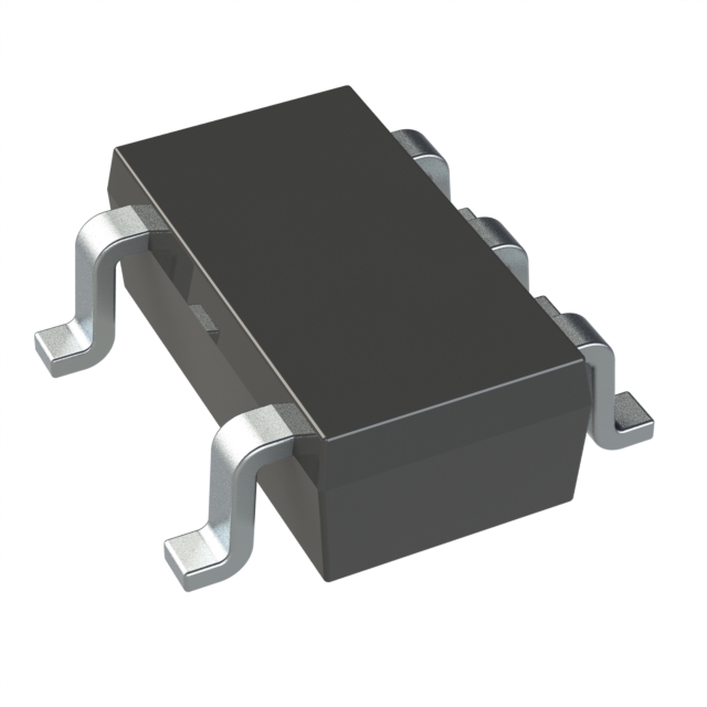
Texas Instruments ESDS312DBVR Package, Pin Configuration, and Channel Routing
Texas Instruments ESDS312DBVR is implemented in the DBV package, which corresponds to the standard SOT-23-5 outline. For this device, pin 2 is the ground reference, pins 4 and 5 are the two protected I/O channels, and pins 1 and 3 are labeled NC. These NC pins are not merely unused terminals in the conventional sense. TI defines them as optional routing aids for straight-through trace implementation, and they may be left floating or tied to ground depending on layout intent.
This pin assignment matters because ESD protection performance is shaped not only by the silicon clamp itself, but also by the current path that surrounds it on the PCB. In high-speed or tightly packed interfaces, every millimeter of additional trace length adds parasitic inductance and capacitance. During an ESD event, that parasitic network can momentarily raise the clamping voltage seen by the protected transceiver, even when the protection diode is nominally fast. A package that allows the signal path to remain direct and continuous reduces detours, minimizes loop area, and improves the odds that surge current is diverted into ground before the downstream IC sees excessive stress.
The ESDS312DBVR package is therefore better understood as part of the protection architecture, not just a mechanical enclosure. With pin 2 placed as the central ground node and pins 4 and 5 assigned to the protected channels, the layout can be arranged so that the I/O lines pass the device with minimal deviation. The optional use of pins 1 and 3 for straight-through routing gives additional flexibility when working with two-line interfaces such as differential signal pairs, low-speed data links, or tightly grouped control lines. That flexibility often simplifies escape routing in dense regions near connectors, where protection components are most effective when placed physically close to the entry point.
From an electrical perspective, clean flow-through routing has several benefits. First, it lowers series discontinuity in the protected path. Second, it avoids sharp meanders that can degrade signal integrity. Third, it keeps the shunt path to ground compact, which is critical because ESD current rises extremely quickly and will exploit every parasitic inductance in the return path. In practice, even a very capable TVS structure can underperform if the ground via is remote or if the protected line must dogleg around the package. The package geometry of the ESDS312DBVR helps reduce that risk by supporting a more linear routing style.
The NC pins also deserve a more precise interpretation. In many components, NC simply means “do not connect.” Here, the recommendation is more nuanced. Since TI permits these pins to float or be grounded, they can be used strategically in layout. If they support a cleaner signal path or a more symmetric channel arrangement, they become useful board-level features. If they are not needed, leaving them inactive does not compromise device function. This kind of packaging choice reflects a practical understanding of real PCB constraints, especially in small consumer, industrial, and embedded designs where trace access is limited and connector placement is fixed early in the design cycle.
For two-channel protection, channel symmetry is another subtle advantage. When both protected lines can be routed with similar geometry, channel-to-channel parasitics tend to remain better matched. That may not matter much for low-speed GPIO protection, but it becomes more relevant for paired interfaces where skew, imbalance, or discontinuity can affect system margins. Even when the ESDS312 is not used on very high-speed links, preserving routing symmetry usually makes the design more robust and easier to validate.
On the manufacturing side, the SOT-23-5 footprint remains a strong practical choice. It is widely supported across assembly lines, familiar to PCB library teams, and easy to source in standard pick-and-place workflows. That reduces risk in both prototype and volume builds. A familiar package also lowers the chance of footprint interpretation errors and generally speeds up board integration, especially when procurement and layout teams are working under schedule pressure. In space-constrained products, SOT-23-5 often provides a useful balance between board area, assembly simplicity, and electrical performance.
A recurring pattern in interface protection design is that nominal device ratings attract most of the attention, while package-enabled routing quality determines much of the real-world result. The ESDS312DBVR is a good example of why that distinction matters. Its DBV / SOT-23-5 implementation, central ground pin, dual protected I/O pins, and optional straight-through use of NC pins together support a layout style that is electrically cleaner and mechanically easier to realize. In many designs, that combination is more valuable than a small difference in datasheet headline parameters, because ESD reliability is won or lost at the boundary between device physics and PCB execution.
Texas Instruments ESDS312DBVR Working Principle in Transient and ESD Events
Texas Instruments ESDS312DBVR is a low-capacitance TVS and ESD protection device designed to remain electrically quiet during normal signal operation and become conductive only when the line voltage moves outside a tightly defined safe region. Its value is not simply that it “clamps” transients, but that it does so with very low parasitic loading and very fast state transition. That combination makes it suitable for interfaces where signal integrity and surge robustness must coexist on the same node.
Under normal operating conditions, the protected I/O line stays within the device’s non-conducting region. In this state, the internal protection structure presents only leakage current and a small parasitic capacitance to the line. From a system perspective, this means the device behaves almost like an open circuit. It does not continuously regulate the signal, does not shape the waveform in a noticeable way, and does not interfere with ordinary data transitions as long as the interface remains inside the allowed voltage window. This passive behavior is the key reason such devices can be placed directly on high-speed or timing-sensitive nets without functioning as an active participant in the signaling path.
The operating principle changes immediately when a transient event pushes the line above the positive protection threshold or below the negative trigger region. At that point, the semiconductor junction network inside the ESDS312DBVR enters conduction and creates a low-impedance discharge path from the stressed node to ground. The transient current is therefore diverted away from the vulnerable downstream circuitry and into the protection path. This is the central mechanism of operation: the device does not prevent the transient from appearing at the connector or trace entry point, but it limits how much of that energy reaches the protected IC input by steering current into a controlled return path.
In transient and ESD conditions, speed is more important than raw power alone. ESD pulses have extremely fast rise times, so a protection component must respond before the protected silicon sees damaging overvoltage. The ESDS312DBVR is engineered for this regime. It transitions from its passive state to its conductive state within nanosecond-scale timing, which is fast enough to intercept the steep front edge of an ESD strike. This fast turn-on is what allows the device to protect modern interfaces whose internal gate oxides and input cells can be damaged long before slower suppression methods become effective.
The internal diode-based topology also explains why the device can handle both positive and negative stress events. For a positive surge, current is shunted from the line to ground through the forward or avalanche conduction path, depending on the instantaneous voltage level and internal structure biasing. For a negative surge, the complementary path conducts and again forces the excess current toward ground reference. In both cases, the protected node is held within a much narrower voltage excursion than would occur without suppression. The line is not held at an ideal fixed voltage, but it is prevented from reaching the destructive extremes that typically cause oxide rupture, junction breakdown, or latch-up in downstream devices.
Texas Instruments specifies the ESDS31x family for high ESD robustness, including very high air-discharge levels such as ±30 kV under standardized test conditions. That specification should be read correctly from an engineering standpoint. It indicates the device can survive and redirect current from severe electrostatic events in a controlled test environment, not that every real-world system will tolerate unlimited surge energy simply by adding this part. Board layout, grounding quality, connector geometry, return inductance, and the dynamic resistance of the protection path all influence actual clamping performance in the final product. In practice, the protection device is only as effective as the current path provided to it.
This point becomes especially important in PCB implementation. If the trace from the connector to the TVS is long, or if the ground connection from the TVS to the reference plane is narrow, vias are sparse, or the return path is inductive, the transient voltage at the protected node can rise significantly before the current is fully diverted. The reason is straightforward: during an ESD pulse, even a small parasitic inductance produces a large voltage according to di/dt. A protection component with excellent intrinsic response can therefore appear much less effective if the layout forces the pulse current through a poor path. A short trace to the protection device, immediate connection to a solid ground plane, and minimal loop area usually improve real clamping behavior more than small differences in datasheet headline ratings.
Another useful way to understand the ESDS312DBVR is to separate static specifications from dynamic behavior. In normal design review, it is common to focus on reverse standoff voltage, breakdown voltage, and capacitance. These are necessary parameters, but they do not fully describe how the device behaves during the first nanoseconds of a real strike. Dynamic resistance, package inductance, and current return topology often dominate the actual peak voltage seen by the protected IC. For high-speed systems, this distinction matters. A part can look ideal on paper yet underperform in layout if the placement is not connector-centric and ground stitching is weak.
For high-speed interfaces, the low-capacitance characteristic is one of the most important design features. Every protection device adds some parasitic capacitance, and that capacitance interacts with line impedance, edge rate, and receiver equalization. If the capacitance is too high, eye diagrams shrink, rise times slow, and insertion loss increases. The ESDS312DBVR is built to keep that effect small enough that the protected line remains functionally transparent in standard operation. This is why such devices are commonly used on USB, high-speed digital I/O, control lines, and other interfaces where both compliance and signal fidelity matter. The practical design challenge is always to place the device close enough to the threat entry point for protection, while keeping the routing clean enough to avoid degrading channel quality.
In application scenarios, the part is most effective at system boundaries. Connectors, exposed cables, test points, external button lines, and sensor interfaces are common injection points for ESD and fast transient energy. Placing the ESDS312DBVR near these boundaries allows the event to be intercepted before the surge propagates deeper into the board. This placement strategy is more effective than locating the device near the protected IC, because once the transient has already traveled across several centimeters of trace, coupling into nearby circuitry and ground bounce may already have occurred. The best suppression strategy is to stop the event at entry, not after distribution.
A recurring observation in robust interface design is that ESD protection should be treated as a current-routing problem rather than a voltage-clamping problem alone. That perspective leads to better implementation choices. The objective is to create a path that the transient current naturally prefers over the path into the sensitive silicon. When the ESDS312DBVR is used this way, it becomes part of a larger electromagnetic containment strategy that includes trace geometry, local reference continuity, and controlled grounding. This system-level view usually produces more reliable hardware than selecting the “strongest” TVS by rating and placing it without regard to return-path physics.
Once the transient event decays and the line voltage returns within the non-trigger region, the ESDS312DBVR exits conduction and returns to its passive state. This recovery occurs quickly, typically on a nanosecond scale, so the interface can resume normal operation without needing reset or bias restoration from the protection device itself. That rapid self-recovery is essential in communication systems and fast digital links, where protection must not create long-lived disturbance after the external event has passed.
Viewed from both mechanism and application, the ESDS312DBVR is effective because it combines three behaviors that are often in tension: near-transparency during normal signaling, very fast conduction during overvoltage stress, and rapid return to the non-loading state after the event. The device protects not by continuously controlling the line, but by remaining dormant until the exact moment a transient escapes the allowed operating envelope. That selective intervention is what allows it to preserve signal integrity in ordinary operation while still providing strong suppression against ESD and surge exposure at the system edge.
Texas Instruments ESDS312DBVR Key Performance Parameters for Design Evaluation
Texas Instruments ESDS312DBVR should be evaluated as a protection element, not as a passive accessory. Its electrical limits, parasitics, and layout sensitivity directly influence whether the protected interface survives real transients without degrading signal quality during normal operation. For design selection, the key parameters are reverse standoff voltage, clamping behavior, capacitance, leakage, and temperature capability, but these values only become meaningful when interpreted in the context of the actual interface, board topology, and downstream IC tolerance.
Reverse standoff voltage is the first screening parameter because it defines the normal operating envelope of the device. ESDS312DBVR is rated for a 3.6 V reverse standoff, which positions it for low-voltage signal lines, GPIO, control lines, and many sub-5 V communication interfaces. The practical check is not simply whether the nominal signal is below 3.6 V. The more important question is whether the line ever spends meaningful time above that level when DC bias, ringing, startup behavior, hot-plug events, and common-mode shifts are included. A nominal 3.3 V rail often looks safe on paper, yet field measurements can show overshoot above the standoff limit during connector insertion, cable discharge, or fast edge transitions coupled through package and trace inductance. In that situation, the protection device can begin to conduct during normal operation, increasing distortion or creating unexpected loading. A robust evaluation therefore starts with oscilloscope captures at the connector and near the protected IC, not only with static voltage tables.
Clamping performance is the next parameter, and it is the one most closely tied to actual survivability. Texas Instruments specifies a clamp of 5 V at 1 A and 5.6 V at 12 A for ESDS312/314 from I/O to ground, with 6.5 V at 25 A for the 8/20 μs surge waveform. These numbers indicate the residual voltage that appears across the protected node while surge current is being diverted. In engineering terms, this residual voltage is what the downstream silicon must survive after the protection device turns on. The important implication is that a low standoff voltage does not guarantee a low clamp during a high-current event. The protection structure must transition from a near-open state in normal operation to a low-impedance shunt during a transient, and that transition always leaves some voltage across the line. If the protected transceiver or processor pin has only a narrow absolute maximum margin, then the clamp voltage must be assessed together with package inductance, ground bounce, and trace impedance. The datasheet clamp value is measured under defined conditions; the board-level peak seen by the IC is often higher when the return path is long or narrow.
This is where layout quality often matters as much as the device itself. A TVS diode with strong clamping characteristics can underperform if the current path from connector to TVS to ground includes excess inductance. Even a few millimeters of poorly placed routing can convert a good protection scheme into a marginal one by adding voltage equal to L·di/dt during fast ESD events. In practice, placing ESDS312DBVR close to the entry point, using a short and wide ground return, and minimizing via count typically improves real clamping more than chasing small differences between similar protection parts. For high-speed connectors, the preferred sequence is usually connector, then TVS, then controlled route to the protected IC. That ordering prevents the transient current from propagating deeper into the board before being diverted.
Capacitance is the parameter that decides whether the device is electrically transparent enough for the target interface. ESDS312DBVR specifies 4.5 pF typical and 5.5 pF maximum line capacitance from any I/O to ground at 1 MHz. Channel-to-channel capacitance variation is 0.05 pF typical and 0.1 pF maximum for ESDS312/314, while line-to-line capacitance is 2.25 pF typical and 2.75 pF maximum. These values matter because the TVS is permanently connected to the signal path and therefore contributes to loading, rise-time degradation, impedance discontinuity, and differential imbalance. For moderate-speed digital lines, this capacitance is usually acceptable. For faster interfaces, especially those with tight eye margins, the effect must be quantified rather than assumed. A few picofarads at the connector can materially change insertion loss and mode conversion, particularly when combined with connector parasitics and common-mode chokes.
The channel matching numbers are more useful than they first appear. In differential interfaces, balance often matters as much as absolute capacitance. Unequal loading between the two lines increases skew and converts differential energy into common-mode energy, which can worsen EMI and reduce receiver margin. The low channel-to-channel variation of ESDS312/314 is therefore a positive attribute for paired signals, provided the PCB routing preserves that symmetry. It is common to select a well-matched protection array and then lose the benefit through asymmetrical fanout or an uneven ground reference near the package. When evaluating eye degradation, it is worth separating device capacitance from layout-induced imbalance; the latter is frequently the larger contributor.
Leakage current is small in this device, specified at only 5 nA typical at 3.6 V bias. This supports use on high-impedance or low-power nodes where standby loading must remain negligible. In many systems, leakage is treated as a minor specification, but it becomes important on battery-powered equipment, precision sense lines, reset pins, and interfaces that rely on weak pull-ups or pull-downs. Very low leakage reduces the risk of bias shift over temperature and avoids adding hidden current paths that complicate low-power mode analysis. The practical value here is stability rather than energy alone. A protection component with low nominal leakage but large temperature drift can still disturb a sensitive line in warm enclosures. ESDS312DBVR’s low baseline leakage gives more room before such effects become design-relevant.
Temperature capability extends from -40 °C to 125 °C ambient, placing the device in the industrial range. This is more than a procurement checkbox. Protection behavior interacts with temperature through leakage drift, dynamic resistance changes, and package thermal conditions during repeated stress events. For networking gear, control modules, and embedded systems in enclosed housings, local board temperatures can approach the upper part of this range even when ambient conditions appear moderate. Using a protection device with industrial temperature support reduces the risk of derating surprises once the system is fully assembled and airflow is constrained. It also aligns better with source-controlled designs that may later be deployed into harsher thermal environments than originally planned.
A more complete design evaluation should connect these specifications to likely application scenarios. For low-voltage GPIO, reset, interrupt, and enable lines, ESDS312DBVR is usually attractive because the 3.6 V standoff, low leakage, and manageable capacitance fit the electrical profile well. For slower communication interfaces and many 3.3 V logic paths, it offers a balanced compromise between protection strength and parasitic loading. For differential links, the device can be suitable when data rate and eye budget tolerate a few picofarads and when channel symmetry is preserved through placement and routing. It becomes less comfortable on interfaces that run very close to the 3.6 V boundary under common-mode excursion, or on high-speed links where every picofarad materially affects return loss and jitter. In those cases, the correct question is not whether the device can function, but whether the interface still meets compliance margin after protection is added.
For source-controlled use, it is wise to define acceptance criteria around system impact rather than copying datasheet values alone. Reverse standoff should be tied to measured maximum steady-state and transient line voltage. Clamp performance should be tied to the absolute maximum rating and transient robustness of the downstream IC, with layout assumptions clearly stated. Capacitance should be linked to an insertion-loss or eye-mask budget. Leakage should be referenced against allowable bias error in sleep and active modes. Temperature should be considered together with the actual enclosure and board hot-spot profile. This method prevents the common mistake of approving a part that matches the datasheet yet behaves differently once assembled into the target hardware.
One useful design habit is to treat TVS validation as a board-level exercise, not just a schematic review item. Bench results often reveal that connector placement, split ground strategy, stitching via density, and reference plane continuity have first-order effects on ESD performance. A protection part such as ESDS312DBVR can look electrically conservative in simulation and still fail to protect adequately if the discharge current is forced through a long return loop. Conversely, when the current path is compact and well-controlled, the device often performs closer to its intended clamping behavior, and signal integrity impact remains predictable. In practice, the most reliable designs are usually the ones where protection selection, signal integrity, and layout are treated as one problem from the start.
Viewed as a whole, ESDS312DBVR is best understood as a low-voltage, low-leakage, moderate-capacitance ESD and surge protection array intended for interfaces that need credible protection without excessive loading. Its 3.6 V standoff suits modern low-voltage rails, its clamp levels are usable for many logic-class inputs, and its capacitance profile is reasonable for a wide range of control and communication lines. The decisive factor is rarely the part in isolation. It is how well its standoff margin, residual clamp voltage, and parasitic capacitance align with the actual electrical behavior of the interface after layout, cabling, and environmental conditions are included.
Texas Instruments ESDS312DBVR Typical End-Equipment and Real Engineering Use Cases
Texas Instruments positions the ESDS312DBVR, and the broader ESDS31x family, for systems that combine dense digital processing with externally exposed interfaces. That positioning is technically well grounded. In products such as Ethernet switches, wireless access points, gateways, printers, DVRs, and NVRs, the dominant reliability problem is rarely inside the core logic domain. It appears at the boundary where controlled on-board signal integrity meets an uncontrolled cable, connector, or user-accessible port. That boundary is where electrostatic discharge, cable-induced transients, and hot-plug disturbance energy enter the design.
The ESDS312DBVR addresses this boundary condition with a focused protection model: two data-line channels in a compact package, low enough loading for high-speed signal paths, and clamping behavior intended to divert transient current away from vulnerable interface silicon. In practical design terms, this type of device is not just a compliance accessory. It is part of the channel architecture. Once external copper leaves the enclosure or reaches a touchable connector, protection must be treated as a first-order signal-path element, alongside impedance control, common-mode behavior, and return-path continuity.
In Ethernet-connected equipment, the need becomes more visible. A gateway or switch port is electrically linked to long cable infrastructure that can behave as both an ESD entry point and a transient energy collector. Even if the PHY itself includes internal protection structures, those structures are optimized for limited on-die robustness, not repeated field-level stress at the connector boundary. A discrete low-capacitance TVS device such as ESDS312DBVR shifts the stress-handling function outward, closer to the threat source. That relocation matters. The earlier the transient current is intercepted, the lower the voltage excursion that propagates toward the PHY pins, magnetics-side circuitry, or adjacent interface components.
The real engineering value is not only in peak voltage clamping. It is in managing current loops and preventing transient energy from spreading across the board. If the protection element is placed very close to the connector and referenced into a low-inductance ground path, the discharge current is given a short, controlled escape route. If that same element is placed farther away, or connected to ground through a long via chain or narrow trace, the package may still respond correctly, but the system-level voltage seen by the protected IC can rise sharply due to parasitic inductance. In many layouts, the difference between passing and marginal ESD performance is less about the nominal TVS specification and more about whether the current path was engineered as carefully as the signal path.
This is especially relevant in Ethernet systems because the interface often sits near magnetics, common-mode chokes, status LEDs, connector shields, and dense routing constraints. Under those conditions, a two-channel device can be more useful than a larger array. A larger array may appear convenient at schematic level, but it can force compromises in placement or route symmetry. The ESDS312DBVR often fits more naturally into narrow interface regions where only two exposed lines need direct protection, or where selective protection is preferred to avoid unnecessary loading on unrelated nets. That package-level efficiency is one of its more practical strengths. Board area is not just a mechanical concern; it directly influences whether the protection device can be placed in the right electrical position.
In access points and gateways, the same principle extends beyond Ethernet. Reset lines, management ports, sideband data paths, and auxiliary external interfaces can all become ESD injection points. These signals may not carry high power, but they often terminate directly into low-geometry digital silicon with very limited fault tolerance. For such lines, low capacitance is critical because signal degradation can appear long before outright failure. Protection that preserves edge rate, timing margin, and protocol eye opening is generally more valuable than aggressive clamping combined with excessive parasitic loading. This is where the ESDS312DBVR class fits well: it is intended for high-speed or timing-sensitive paths where the protection device must remain electrically quiet until a transient event occurs.
Printers, DVRs, and NVRs illustrate a slightly different field reality. These systems often expose multiple connectors in a compact enclosure and are frequently subjected to repetitive cable insertion, servicing, or direct contact near the ports. In these products, many failures are not catastrophic in the immediate sense. The system may continue operating, but interface reliability degrades over time, or intermittent communication faults emerge after repeated stress. That pattern is common when small transient events repeatedly couple into PHYs, transceivers, or control processors without causing instant destruction. External ESD suppression reduces this cumulative stress burden. In that role, the device improves not only formal immunity but also long-term service stability.
A subtle but important point is that two-channel protection aligns well with real interface partitioning. Many exposed links are naturally organized as differential pairs, paired control lines, or two critical signals within a larger connector. Using a compact two-line TVS allows protection to match the electrical function rather than forcing an oversized array into the design. This often leads to cleaner routing, lower stub length, and better control of channel parasitics. In practice, protection devices become easier to justify when they do not distort the topology they are meant to secure.
For general-purpose high-speed data lines, ESDS312DBVR is particularly effective in edge-connector zones, daughtercard interfaces, or small mezzanine boards where space is constrained and every parasitic element has visible impact. In these layouts, it is usually better to protect the truly exposed and truly sensitive nets with a tightly placed two-channel solution than to scatter a broader array across a region with compromised return paths. A compact protector tends to preserve routing freedom, which in turn preserves signal quality. This tradeoff is often underestimated early in design, when schematic simplicity is valued more than placement physics.
From a mechanism standpoint, the device should be viewed as part of a coordinated protection stack rather than a standalone shield. Connector design, shield grounding strategy, chassis reference, common-mode filtering, isolation elements, and PCB layer transitions all affect the stress seen by the TVS and the residual energy seen by the protected IC. In Ethernet equipment, for example, a well-chosen TVS cannot compensate for a poorly controlled connector-to-ground discharge path. In printer or surveillance equipment, interface robustness is often determined by how the port region handles current spreading into digital ground, especially when multiple connectors share a constrained perimeter. The most reliable designs treat TVS placement, grounding, and partitioning as one problem.
One recurring lesson in compact interface boards is that low-capacitance protection only delivers its full benefit when the layout avoids unnecessary branch length between connector and protector. The preferred routing order is usually connector first, protection second, protected IC third, with the clamp return tied into ground using the lowest inductance path available. Where possible, direct via stitching near the ground pin is more effective than relying on a longer lateral ground trace. That approach reduces overshoot during fast ESD events and limits cross-coupling into nearby channels. On dense boards, this kind of detail often matters more than choosing between two otherwise similar protection parts.
Another practical consideration is channel selectivity. Not every external pin deserves identical protection treatment. Some lines tolerate more capacitance. Some have internal isolation. Some are not truly exposed in the system’s usage model. The ESDS312DBVR becomes attractive when the design calls for protection exactly where it is needed and nowhere else. That is a more disciplined approach than populating large arrays by default. Targeted protection usually yields better electrical performance, lower board congestion, and fewer unintended interactions with high-speed interfaces.
In that sense, the strongest use case for ESDS312DBVR is not merely “two lines need ESD protection.” It is that two exposed, performance-sensitive lines need protection that can be physically located at the interface boundary without consuming disproportionate area or adding avoidable loading. That makes it well suited to Ethernet-adjacent circuits, service ports, control pairs, compact connector banks, and other tightly routed external interfaces found in networked embedded equipment. When used with disciplined grounding and connector-region layout, it becomes a precise tool for improving field robustness while preserving signal integrity, which is exactly where discrete interface protection earns its place in a mature design.
Texas Instruments ESDS312DBVR PCB Layout and Implementation Considerations
Texas Instruments positions the ESDS312DBVR as a low-capacitance ESD protection array intended to sit directly in the signal path, and that placement guidance is not just a packaging convenience. For a TVS-based protection device, PCB layout is part of the protection element itself. The silicon may define the clamping behavior, but the actual surge current path is completed by copper geometry, via structure, reference plane quality, and local parasitics. In practice, the protection result is determined as much by the layout loop as by the device datasheet.
The primary implementation goal is to intercept transient energy at the point of entry and shunt it to ground before the surge propagates into the protected circuit region. That means the ESDS312DBVR should be placed physically close to the connector, cable interface, or external exposure point rather than close to the vulnerable IC. This distinction matters. If the device is placed near the receiver instead of near the entry point, the transient current can travel across part of the PCB before being clamped, exposing internal traces and adjacent structures to fast overvoltage stress. A protection component that is electrically correct but physically misplaced often underperforms in system-level testing.
The package supports a flow-through routing style, which is especially useful for high-speed or impedance-sensitive lines. One side of the device can accept the incoming trace from the external interface, and the opposite side can continue toward the protected transceiver or processor input. This minimizes routing detours and reduces stub formation. For signal integrity, that is important because every unnecessary bend, neck-down, or branch segment adds parasitic inductance and capacitance. For transient suppression, it is equally important because excess parasitic inductance raises the effective clamping voltage during fast ESD events. At nanosecond time scales, even a short extra trace can materially change peak stress seen by the downstream IC.
The ground connection deserves the highest layout priority. The ESDS312DBVR uses a dedicated ground return pin as the discharge path for transient current, so that pin must connect into a low-impedance reference with minimal loop area. The preferred implementation is a very short trace or, ideally, a direct via transition into a solid ground plane placed adjacent to the device. If board stack-up allows it, one or more stitching vias near the ground pin further reduce inductive impedance and spread the discharge current into the plane more effectively. This is one of the most common differences between a design that passes contact discharge comfortably and one that shows intermittent resets or latent failures under the same test level.
A useful way to think about the layout is to treat the protected line and the ground return as a high-frequency current loop rather than as independent nets. ESD current does not behave like a slow DC event. It follows the path defined by instantaneous impedance, and that path is dominated by inductance during the initial edge. A long, thin ground trace may appear electrically connected in CAD, but during an ESD strike it can force the clamp voltage much higher than expected. In many boards, the limiting factor is not the clamp device itself but the inductive voltage developed between the device ground pin and the true local ground reference of the protected IC.
For paired or differential interfaces, the ESDS312DBVR offers an additional advantage through low channel-to-channel capacitance variation. That characteristic helps preserve skew balance and common-mode behavior, but it does not eliminate the need for disciplined PCB symmetry. Differential routing should remain tightly matched in trace length, geometry, and reference continuity through the protection region. If one line takes a longer or less direct route into the array, or if one channel sees a different via count or plane transition, the pair can accumulate enough imbalance to degrade eye opening, increase mode conversion, or worsen EMI behavior. In lower-speed designs the effect may be subtle, but in faster interfaces it can become measurable very quickly.
This is where the flow-through concept should be used carefully rather than mechanically. A common mistake is to place the protection array in a way that satisfies connector proximity but forces one member of a differential pair into an awkward jog. The better approach is usually to solve placement and orientation together: align the device so both channels can pass through with nearly identical geometry, and ensure the ground pin still has the shortest possible path to the plane. That often requires rotating the package or shifting adjacent components slightly. Small physical adjustments at this stage usually save much larger signal-integrity effort later.
Because the ESDS312DBVR is passive, it does not require a bias supply or control rail. That simplifies integration and removes a class of failure modes associated with powered protection elements, such as incorrect bias sequencing or supply collapse during transients. It also means the device behavior is largely local and immediate, which is beneficial in compact interfaces where protection must remain effective regardless of system power state. In products exposed to cable hot-plug events or operator-induced discharge when the system is off, passive protection at the interface is often the more robust baseline strategy.
That simplicity, however, should not lead to the assumption that the device is electrically invisible. Even low-capacitance protection arrays introduce finite loading, and on high-speed lines the interaction between line impedance, package parasitics, and pad geometry should be considered as a single discontinuity. For many interfaces the effect is small enough to be acceptable without extensive tuning, but once data rates rise or margin becomes tight, the implementation around the device matters more than the nominal capacitance number. Pad size, solder mask definition, anti-pad clearance, and reference plane continuity can contribute as much to insertion loss or reflection as the protection element itself.
A practical layout pattern that tends to work well is straightforward: place the ESDS312DBVR immediately behind the connector pins, route each exposed signal through the device in a straight path, tie the ground pin into the nearest solid ground region with the shortest possible connection, and avoid routing the transient return through shared narrow necks or fragmented copper. If the board uses multiple ground domains, the clamp should return to the same low-impedance chassis-referenced or interface ground strategy used for other entry-point protection elements. Splitting that return path or forcing it through a long internal detour usually reduces protection effectiveness and can inject noise into unrelated circuitry.
Another implementation detail worth attention is via placement. A single distant ground via can satisfy schematic intent but still perform poorly under IEC-style discharge conditions. Moving the via directly adjacent to the ground pin, or adding a second via when space permits, often produces a disproportionate improvement because it lowers effective inductance right where peak current is highest. This kind of change rarely appears dramatic in the layout database, yet it often shows up clearly in compliance behavior. In board reviews, these millimeter-scale adjustments are frequently more valuable than changing to a nominally stronger clamp with a less optimized footprint.
Signal return continuity should also be preserved through the protection area. If the protected traces cross reference plane gaps, slot edges, or cutouts near the array, both signal quality and transient control degrade. The line then loses a clean return path during normal operation, while the protection current is forced into a more complex and inductive route during an ESD event. Keeping the device over a continuous reference plane is usually the safest implementation. When that is not possible, the protection strategy should be reconsidered at the stack-up level rather than patched with longer surface routing.
For dense boards, thermal relief patterns on the ground connection can also become an unintended weakness. They help solderability, but for an ESD discharge path they add impedance. If assembly rules allow it, a more direct copper attachment from the ground pin to the plane is generally preferable for the clamp node. This is a small but meaningful example of how manufacturing conventions and transient-performance goals can conflict. The right balance depends on process capability, but the protection path should not be treated like an ordinary low-current net.
From an application standpoint, the ESDS312DBVR fits best where two signal lines require low-capacitance, board-level ESD protection without adding power dependencies. Typical use cases include differential data interfaces, paired control lines, compact external ports, and sensor or communication links that leave the enclosure boundary. In these scenarios, the device works well when it is treated as an interface structure, not just a schematic symbol. The most reliable implementations usually come from designing the connector, protection array, return path, and receiver entry as one compact electromagnetic region.
The central design principle is simple: the clamp must win the race against the transient. Achieving that is less about adding complexity and more about reducing delay and impedance in the discharge path. Close placement to the entry point, symmetric routing through the protected channels, and an aggressively short ground return are the decisions that most directly determine whether the ESDS312DBVR behaves like an effective first-line protector or merely like a component that was placed near the interface.
Texas Instruments ESDS312DBVR Reliability, Temperature Range, and Compliance Information
Texas Instruments ESDS312DBVR carries a set of reliability, environmental, and compliance characteristics that are directly relevant to component qualification, manufacturing control, and long-term field use. For design teams, these parameters are not just checklist items. They influence assembly flow, storage strategy, derating decisions, and the level of confidence that can be assigned to the device when deployed in exposed interfaces.
From a regulatory standpoint, the device is identified as RoHS compliant under RoHS 3 and marked as REACH unaffected. In practical supply-chain terms, this reduces friction during material declaration review and simplifies inclusion in assemblies that must pass environmental compliance screening across multiple regions. It also lowers the documentation burden during procurement audits, especially in programs where approved vendor lists are tied to substance reporting discipline. While these declarations do not by themselves guarantee fitness for every regulated end market, they remove a common source of procurement delay and support smoother part approval in mainstream industrial and embedded designs.
Moisture Sensitivity Level is specified as MSL 1. This is one of the most favorable handling classifications for surface-mount manufacturing because it indicates effectively unlimited floor life under standard factory ambient conditions after the package is opened. That has direct operational value. It reduces the need for dry-pack tracking discipline, minimizes bake requirements, and makes the part easier to manage in mixed-volume production where reels may remain partially used for extended periods. In assembly environments, this kind of package robustness often matters more than expected, especially when line interruptions, kitting delays, or service-build variability make strict exposure control difficult. Parts with MSL 1 behavior generally create fewer hidden process risks than more moisture-sensitive alternatives.
The operating ambient temperature range of -40°C to 125°C places ESDS312DBVR comfortably within the envelope expected for industrial-grade electronics. This range supports deployment in systems exposed to cold start conditions, elevated enclosure temperatures, and localized heating from nearby power components. The storage range of -65°C to 155°C provides additional margin for warehousing, transport, and non-operational environmental stress. These values should be read as survivability and functionality limits, not as a recommendation to operate continuously at the extremes without thermal review. In practice, TVS devices often sit quietly in the circuit for most of their life, but when a surge event occurs, local junction heating can rise sharply for a short duration. That makes the surrounding thermal environment more important than static ambient numbers alone may suggest.
Texas Instruments lists a junction-to-ambient thermal resistance of 163.9°C/W for the ESDS312 in the DBV 5-pin package. For a transient suppression device, this number is easy to overlook because normal operation does not usually involve meaningful steady-state dissipation. Still, it is useful in two engineering contexts. First, it helps estimate junction temperature rise if the device is exposed to repetitive leakage-related stress, abnormal line bias, or fault conditions that create sustained current flow rather than short impulses. Second, it gives a rough boundary for understanding how quickly thermal margin can be consumed in dense layouts with poor copper spreading or elevated local board temperature.
A common design mistake is to treat a TVS diode as thermally irrelevant because its main job is pulse clamping. That assumption is only safe when surge events are infrequent, pulse energy is within rating, and post-event recovery is complete. In real systems, the more difficult cases involve repetitive disturbances, cable discharge events, or power-cross faults that stretch beyond the idealized waveform used in datasheet surge tests. Under those conditions, package thermal impedance and board heat extraction begin to matter. Even a small package can become a limiting factor if the protection network is asked to absorb energy repeatedly with little cooling interval. For that reason, board-level placement should favor short current return paths and enough copper to avoid turning the TVS into an isolated thermal hotspot.
The specified JEDEC handling-related ESD ratings are ±2500 V HBM and ±1000 V CDM for all pins. These values indicate a reasonable level of robustness during manufacturing, handling, and automated assembly. They are relevant to factory process control because they reflect device survivability against the types of electrostatic events associated with contact handling and charged-device scenarios. In procurement and quality discussions, these JEDEC ratings help establish that the component meets standard expectations for assembly resilience and is not unusually fragile relative to typical semiconductor handling requirements.
It is important, however, to separate component-level ESD robustness from system-level protection performance. HBM and CDM describe how the device itself tolerates manufacturing-related electrostatic events. They do not predict how well the protected interface will survive IEC 61000-4-2 strikes in an end product. That distinction often gets blurred in early part selection. A device can have adequate JEDEC handling ratings and still perform poorly in a board-level IEC event if layout inductance is excessive, grounding is weak, or the protected trace reaches the IC before the clamp engages effectively. In protection design, the datasheet numbers are only the starting point. Physical implementation determines whether the intended clamping behavior is realized during the actual transient.
This is where experience with TVS deployment becomes decisive. If the ESDS312DBVR is placed too far from the connector, the trace inductance between the entry point and the diode can generate a significant voltage overshoot before current is diverted. If the return path to ground is narrow, long, or shared with sensitive circuitry, the clamping action may inject noise into internal references and create failures that look unrelated to ESD at first glance. Good results usually come from placing the TVS at the disturbance entry point, keeping the protected path straight, and tying the return into a low-impedance ground structure with minimal loop area. In many cases, layout quality changes system survival margin more than switching to a nominally stronger suppressor.
Another practical point is that the -40°C to 125°C operating range should be interpreted together with surge behavior, not independently. Semiconductor clamping characteristics drift with temperature. Leakage current, dynamic resistance, and trigger-related behavior can shift enough to alter margin in tightly constrained interfaces. A design that looks comfortable at room temperature may become less forgiving at high ambient, especially if the line already runs near its maximum allowable signal or common-mode limits. It is usually better to reserve electrical headroom than to optimize the protection network too close to nominal values. Conservative headroom tends to pay off in validation, especially when cable variation, connector wear, and grounding uncertainty are added to the test setup.
From a qualification perspective, the ESDS312DBVR presents a favorable combination of compliance clarity, easy manufacturability, industrial temperature coverage, and credible handling robustness. MSL 1 simplifies floor operations. RoHS 3 and REACH status ease environmental review. The JEDEC ESD ratings support normal assembly expectations. The thermal data, while secondary to surge specifications, should still be part of fault-energy analysis and placement strategy. Taken together, these attributes make the device straightforward to approve for a wide range of embedded and industrial designs, provided the selection process remains grounded in actual surge paths, thermal context, and board-level implementation discipline rather than datasheet headline values alone.
Texas Instruments ESDS312DBVR Potential Equivalent/Replacement Models
Texas Instruments ESDS312DBVR is a 2-channel TVS/ESD protection device positioned for data-line protection where low capacitance, compact routing, and strong transient robustness must coexist. Inside the TI portfolio, the most relevant adjacent options are ESDS311 and ESDS314. These devices belong to the same protection family, so the replacement discussion is not primarily about protection philosophy changing from one part to another. It is about how many lines must be protected, how the lines are routed through the board, and whether the electrical parasitics and package geometry still support signal integrity and manufacturability.
The most immediate selection variable is channel count. ESDS311 is the single-line variant. ESDS312DBVR covers two lines. ESDS314 extends protection to four lines. This seems trivial at first glance, but in practice it drives both the electrical and physical optimization of the design. A single-line protector like ESDS311 avoids stranded channels and can reduce leakage aggregation in sparse protection schemes. A four-line part like ESDS314 can compress BOM count and reduce placement area when multiple I/O nodes are clustered. ESDS312DBVR sits in the middle and is often the most balanced choice for differential pairs, adjacent control lines, or dual-interface entry points where symmetry and routing simplicity matter more than raw channel density.
From a protection-network perspective, these parts solve the same class of problem: clamp fast ESD events and surge energy before that stress reaches a vulnerable transceiver, MCU pin, FPGA bank, sensor interface, or connector-adjacent analog front end. The critical mechanism is not only the peak clamping action, but also how little the protection element disturbs the line under normal operation. That is why low capacitance is central to this family. With capacitance around the low-pF range, the device can remain transparent enough for many data-line applications while still delivering meaningful transient suppression. In actual layouts, this balance is often more important than absolute headline ESD rating. A stronger clamp with excessive capacitance can quietly degrade edge rate, eye opening, or analog settling long before any ESD event occurs.
For replacement decisions, electrical equivalence should be treated as multidimensional rather than a simple datasheet parameter match. Reverse standoff voltage is one axis. ESDS312DBVR is built around a 3.6 V reverse standoff level, so substitute parts must remain safely non-conductive across the highest normal signal excursion, including overshoot, supply tolerance, startup behavior, and hot-plug transients. A part that nominally looks close but begins to load the line during routine operation can create intermittent failures that are difficult to isolate. This tends to show up first in interfaces with weak drivers, marginal logic thresholds, or elevated operating temperature.
Capacitance is the second axis, and it deserves more scrutiny than it typically receives. A value near 4.5 pF per channel may be acceptable in many low- to moderate-speed interfaces, but whether it is acceptable depends on where the protector sits in the channel and what source impedance drives it. Protection placed directly at a connector usually has less impact than the same part dropped mid-route on a weak or high-impedance signal. In differential-line use, the parasitic symmetry between channels also matters. Even if two devices share similar nominal capacitance, package and routing asymmetry can convert that into common-mode disturbance or skew. This is one reason ESDS312DBVR often remains the cleaner option for paired-line protection: the 2-channel structure aligns naturally with compact flow-through routing, reducing the layout penalty that can erase the benefit of a theoretically equivalent alternative.
Surge and ESD ratings form the third axis. A practical substitute should preserve the same order of robustness: up to 25 A for an 8/20 µs surge waveform and IEC 61000-4-2 protection up to ±30 kV. These numbers are useful, but they should not be read in isolation. Real-world protection performance depends strongly on loop inductance between connector, TVS device, and return path. A device with a strong datasheet rating can underperform if placed too far from the entry point or connected through narrow traces with poor ground return geometry. In board bring-up, the most resilient designs usually place the TVS element as the first intercept point at the board edge, with a short and low-inductance discharge path to reference. The device choice and the layout are inseparable; treating them independently often leads to false confidence.
Package compatibility is the next hard constraint. ESDS312DBVR and ESDS314 both use 5-pin SOT-23 style packaging, while ESDS311 uses a 2-pin SOD323 package. That means ESDS311 is not a footprint drop-in for ESDS312DBVR, even if the application only needs one protected line. The substitution becomes a schematic and PCB redesign, not a procurement-level swap. ESDS314 may appear mechanically closer because it shares the SOT-23 family, but pinout and channel mapping still need careful verification. In compact layouts, even minor pin assignment differences can force trace crossover, via insertion, or longer line stubs, all of which work against signal integrity and transient containment. In many high-density designs, the package is not just a mechanical shell; it is part of the routing strategy.
This is where the phrase “easy flow-through routing” becomes more meaningful than marketing shorthand. For paired lines, especially those entering from a connector and continuing inward to a transceiver, a 2-channel arrangement can minimize trace bending, stub creation, and asymmetrical detours. That usually translates into cleaner impedance control and lower discontinuity energy. In practice, a nominally denser 4-channel part is not always better, because consolidating more channels into one package can force non-ideal line entry angles or channel remapping. When protecting exactly two related lines, ESDS312DBVR often represents the local optimum between protection density and routing elegance. That local optimum is easy to lose when replacement is driven only by availability.
When evaluating non-TI alternatives, the comparison should remain disciplined. At minimum, the replacement should match the unidirectional topology, 3.6 V reverse standoff voltage, low capacitance around 4.5 pF per channel, 25 A 8/20 µs surge capability, ±30 kV IEC 61000-4-2 ESD robustness, appropriate channel count, and package/footprint constraints. But a better screening method goes one step further and asks how the candidate behaves in the specific interface context. For USB low/full-speed, GPIO, UART, RS-485 support nodes, sensor lines, or other moderate-speed paths, the capacitance window may be forgiving. For faster or more timing-sensitive links, dynamic resistance, clamping voltage under realistic pulse current, and package-induced parasitics begin to matter more than nominal VRWM alone. The strongest replacements are those that preserve both the protection envelope and the original signal-path assumptions.
A practical way to think about these three TI options is to map them to board topology rather than just line count. ESDS311 fits isolated, single-node exposures such as one interrupt line, one reset input, or one external sense point. ESDS312DBVR fits paired structures such as differential signals, two-wire interfaces, or side-by-side connector pins where routing continuity is important. ESDS314 fits grouped I/O clusters where several exposed lines converge in a tight area and some routing flexibility exists. This topology-first approach usually yields better substitution choices than a pure datasheet-first approach, because ESD protectors influence the board as physical components as much as they do as electrical clamps.
One recurring issue in replacement work is assuming that “same family” means “same behavior under abuse.” It often means similar intent, not identical dynamic performance. Clamp voltage versus pulse current, leakage spread over temperature, and the interaction with upstream series resistors or common-mode chokes can shift enough to affect margin. Designs that passed compliance comfortably with one TVS may become borderline with another if the routing or return path changes at the same time. That is why the most reliable replacement process includes three checks in sequence: schematic equivalence, footprint and pinout verification, and then layout-current-path review. Skipping the third step is a common source of late-stage surprises.
For engineers selecting a replacement under supply pressure, ESDS311 is the logical alternative when only one line is genuinely exposed and a board respin is acceptable. ESDS314 is the logical alternative when more than two lines need protection or when BOM consolidation outweighs the routing penalty. If the original design depends on compact, symmetrical, two-line protection with minimal layout disturbance, ESDS312DBVR usually remains the most technically coherent choice. That is not conservatism; it reflects a broader principle in protection design: the best TVS device is often the one that disappears into the signal path during normal operation and dominates it only during the transient event. ESDS312DBVR is well aligned with that role when the protected structure is inherently two-channel.
Conclusion
Texas Instruments ESDS312DBVR is a compact 2-channel unidirectional TVS diode array designed for low-voltage interfaces that must survive repeated transient stress without degrading signal integrity. Its value is not defined by a single headline parameter, but by the way several electrical characteristics align for real interface protection: high IEC 61000-4-2 robustness up to ±30 kV, 25 A surge capability under an 8/20 µs waveform, typical line capacitance of 4.5 pF, low leakage current, and a small SOT-23-5 footprint suitable for dense layouts. This combination makes it particularly effective on interfaces where board area is limited, the signal path is moderately fast, and transient exposure is not theoretical but expected during handling, cable insertion, or field operation.
At the device level, ESDS312DBVR works by clamping transient energy before it propagates into vulnerable IC pins. In normal operation, the array presents very low leakage and limited parasitic loading, so the protected line behaves close to its native condition. During an ESD or surge event, the diode structure turns on rapidly and diverts current to the reference rail, restricting the voltage seen by the downstream transceiver, MCU input, PHY, or connector-side logic. This mechanism is straightforward in principle, but protection effectiveness in practice depends on dynamic behavior rather than only static breakdown numbers. The important engineering question is not just whether the TVS conducts, but how quickly it enters conduction, what clamping level it sustains under realistic current, and how much residual stress remains at the protected node after package and PCB parasitics are included.
That is where ESDS312DBVR sits in a useful middle ground. It is not an ultra-low-capacitance specialist for multi-gigabit differential links, and it is not an oversized surge suppressor intended for power rails or harsh industrial line interfaces. It is better understood as an efficient protection element for everyday high-exposure signal nets operating in the low-voltage domain. Ethernet sideband lines, USB 2.0 signals in constrained designs, GPIO routed to external headers, interrupt lines, control buses with moderate speed, and similar nets all fit this profile well. In these cases, excessive capacitance would distort edge rates or eye margins, while weak protection would leave the system exposed to real-world discharge events. The ESDS312DBVR balances these two constraints with relatively little compromise.
Its 4.5 pF typical capacitance is especially relevant in product selection. For many low-speed and mid-speed digital lines, this level is low enough to preserve timing margins if layout is disciplined and trace lengths are controlled. In USB 2.0 and other edge-sensitive interfaces, the device can still be viable, but placement becomes decisive. A recurring pattern in successful implementations is to place the TVS array immediately adjacent to the external connector so that transient current is intercepted at the entry point rather than after the pulse has already spread across the board. Even a strong TVS can underperform if it is placed several centimeters away with narrow return paths, because the inductive voltage developed in the trace between connector and clamp can dominate the residual stress seen by the protected IC. In other words, board geometry often determines whether a good protector behaves like a good protector.
The 25 A 8/20 µs rating broadens its usefulness beyond pure ESD compliance. Many designs encounter a mix of threats: cable discharge events, electrically fast transients from nearby switching activity, and lower-energy surge-like disturbances coupled through external wiring. A device that only addresses air and contact discharge may pass bench tests yet still leave intermittent field failures. ESDS312DBVR offers a more rounded suppression profile, which is valuable in products deployed outside tightly controlled environments. That does not make it a substitute for dedicated surge architecture on exposed industrial ports, but it does reduce the gap between lab compliance and actual operating resilience.
The unidirectional topology also matters. It is well suited for signal lines referenced to ground in systems where negative excursions must be clamped aggressively and positive excursions remain within a low-voltage operating window. For GPIO, reset lines, logic-level communication lines, and many USB-adjacent or controller-side nets, this is a practical choice. If the protected line swings significantly below and above ground as part of normal signaling, or if the interface uses AC-coupled or truly bipolar behavior, a bidirectional device may be more appropriate. This distinction is often overlooked during part selection, yet it strongly affects both signal fidelity and clamp behavior during abnormal conditions.
From a portfolio perspective, the ESDS312DBVR benefits from clear positioning within the TI ESDS31x family. That helps in design scaling. If the architecture evolves from one protected pair to multiple channels, or if capacitance and clamping priorities shift, migration within the same family can simplify qualification and sourcing. For engineering teams, that continuity reduces redesign friction. For procurement, it improves second-phase planning because package style, vendor alignment, and application intent remain consistent across related options.
The SOT-23-5 package is another practical advantage. It is small enough for dense consumer and embedded layouts, but still large enough to support predictable assembly and inspection in standard SMT flows. In compact connector regions, that matters more than it first appears. Protection components are frequently added late in the layout cycle, and larger packages can force rerouting or compromise return-path quality. A small dual-line array such as ESDS312DBVR can often be inserted near the connector with minimal disruption, which increases the chance that protection is implemented correctly rather than merely included schematically.
In application use, the part is most compelling when two lines need symmetrical protection with minimal board penalty. USB D+ and D−, paired control lines, clock-plus-data pairs in moderate-speed domains, or dual GPIO exposed through a cable or header are obvious examples. It is also effective on interfaces that are not traditionally viewed as high risk but become failure points due to user interaction, such as test pads, debug connectors, and low-cost I/O headers. These nets often survive validation until enclosure handling, cable hot-plug behavior, or production fixtures introduce repeatable discharge paths. In those situations, adding a compact TVS array close to the access point often resolves failures that would otherwise appear random at the system level.
One useful selection principle is to evaluate ESDS312DBVR not only by whether it “fits” the nominal signal speed, but by the quality of the system margins after protection is added. If the interface already operates close to its timing or eye-limit budget, even a modest parasitic load can become significant. If the interface has comfortable margin but poor field robustness, stronger protection usually provides a better return than pursuing the absolute lowest capacitance. This tradeoff is central in practical design work. Excessive emphasis on capacitance alone often leads to under-protected products, while excessive emphasis on surge rating can silently erode signal quality. ESDS312DBVR is attractive because it avoids both extremes for a large class of common embedded and communication interfaces.
For sourcing and lifecycle planning, the part also presents a stable proposition. TI branding, industrial temperature support, standard packaging, and a clearly defined use case all contribute to lower integration risk. That does not remove the need for validation, but it does make the validation process more predictable. In transient protection, predictability is valuable because failures are often nonlinear and layout-sensitive. Devices with balanced, well-documented behavior generally shorten the path from prototype to compliant production hardware.
Texas Instruments ESDS312DBVR is best viewed as a focused protection component for designers who need credible transient immunity on two low-voltage signal lines without paying heavily in capacitance, cost, or area. It is particularly strong in connector-facing signal protection where ESD exposure is frequent, bandwidth is important but not extreme, and layout discipline can be maintained. When placed correctly and matched to the signal environment, it delivers a robust protection envelope that is disproportionate to its size, which is exactly why parts in this class remain so useful across embedded, industrial, and communication designs.