 >
>


Product overview: VIPER06HSTR series by STMicroelectronics
In the landscape of high-voltage offline PWM switching ICs, the VIPER06HSTR series by STMicroelectronics represents a synthesis of power integration and control sophistication, purpose-built for low-power AC-DC converter design. At its core, the VIPER06HSTR incorporates an internally connected 800 V N-channel MOSFET, tightly coupled with optimized controller logic, effectively eliminating the need for discrete external switching devices and streamlining PCB layout. This monolithic integration reduces parasitic elements, improves EMI performance, and enables high-voltage start-up directly from the line input—a distinct advantage for compact offline designs.
The controller architecture embodies an advanced PWM scheme with current mode control, affording robust line and load regulation across diverse operating conditions. This facilitates precise output voltage management, while enhancing reaction speed in transient scenarios typical of load switching in embedded metering and industrial automation. Proprietary control algorithms manage burst mode operation at light loads, sharply reducing standby power consumption, which is pivotal for meeting stringent energy consumption standards in modern consumer and utility platforms.
Topology flexibility defines the VIPER06HSTR; both buck and flyback configurations benefit from dedicated features such as integrated startup circuitry, internal feedback compensation, and protection mechanisms including overload, thermal shutdown, and short-circuit resilience. By compressing these functional blocks into a single SSOP-10 footprint, design time is measurably reduced, BOM complexity drops, and manufacturability increases. Field deployments frequently call for adaptive converter platforms where form factor and electrical isolation requirements differ—this IC adapts with minimal redesign effort. In typical metering infrastructure, reliable performance under voltage surges and extended temperature ranges ensures long-term operational stability, directly impacting maintenance cycles and system reliability.
From an engineering perspective, the reduction in external components not only minimizes assembly errors but also accelerates regulatory compliance for safety standards such as IEC and UL, especially in applications exposed to hazardous voltages. The VIPER06HSTR’s internal logic sequencing grants automated recovery during fault events, removing the necessity for additional supervisory circuitry. This has demonstrated significant improvement in first-time pass rates during field qualification, lowering overall system cost and deployment risk.
An implicit insight arising from practical deployment is the IC’s ability to handle design margin tolerances gracefully, even with wide supply variations and episodic load spikes. This resilience, coupled with its unified controller-MOSFET architecture, makes the device particularly effective in segmented industrial supply rails and distributed power architectures, where reliability and space efficiency are non-negotiable. The VIPER06HSTR series signals a pivotal shift towards smarter, denser AC-DC solutions, directly supporting the continuing evolution of compact, energy-compliant electronic systems.
Key application scenarios for VIPER06HSTR
VIPER06HSTR integration directly addresses power supply modernization challenges across several domains. By supporting rectified mains input without requiring an auxiliary winding, the device streamlines power stage layouts, sharply reducing component count and footprint. This mechanism improves thermal management and diminishes leakage paths, maximizing board space utilization—a critical advantage for dense embedded designs like smart utility meters and compact home appliance controllers.
Energy conservation is central to VIPER06HSTR’s appeal. Its advanced standby performance and low quiescent consumption enable compliance with stringent global efficiency standards. In real-world LED driver deployments, minimizing standby losses directly extends product life and lowers operational costs. The device’s inherent reliability further supports robust operation under wide input voltage conditions, preventing failures in fluctuating mains environments typical of legacy building infrastructures.
Migration from capacitive supplies to VIPER06HSTR-based topologies introduces significant improvements in electromagnetic compatibility and lifetime expectancy. Engineers frequently observe reductions in both audible and electrical noise, as the controller’s switching profile and protection features shield sensitive loads. In power metering systems, this translates to high signal integrity and reduced calibration drift, ensuring consistent measurement accuracy over time.
A nuanced advantage emerges in maintenance and upgrade scenarios. The VIPER06HSTR’s architecture allows for drop-in circuit enhancements with minimal hardware rework, facilitating rapid prototyping and cost-effective field retrofits. This adaptability promotes incremental advances in platforms ranging from appliance power modules to interconnected IoT endpoints—all while sustaining strict budgetary and design constraints.
Careful exploitation of these characteristics enables reliable, high-efficiency supplies within form-factor-constrained products. By leveraging direct mains operation, system architects eliminate the traditional tradeoff between performance and miniaturization. This convergence of reliability, low consumption, noise suppression, and design flexibility marks VIPER06HSTR as a foundation for next-generation embedded power conversion.
Core features and functional architecture of VIPER06HSTR
The VIPER06HSTR is engineered as an integrated high-voltage converter, where robustness and EMI mitigation drive its core architecture. Central to its foundation is an 800 V power MOSFET fully integrated with a PWM controller; this hybrid topology ensures a compact footprint and enhances electric stress tolerance, particularly in demanding industrial and grid-connected environments. The on-chip PWM controller features frequency jittering, a technique that dynamically varies the switching frequency to distribute electromagnetic energy across the spectrum. This substantially reduces peak EMI emissions and simplifies downstream filtering, which translates to more straightforward PCB layout and lower system-level compliance costs.
The current control loop is tightly managed via user-settable, cycle-by-cycle current limiting. This hardware-level intervention enables deterministic fault response, preventing MOSFET overstress and ensuring rapid recovery after abnormal load events. Rather than relying on discrete shunt resistors, the device leverages a lossless SenseFET scheme for current sensing. This approach embeds a scaled-down replica MOSFET within the die, mirroring the main switch's conduction profile with high temporal precision and zero insertion loss, thus maintaining efficiency and accuracy even as system temperature fluctuates.
Thermal management is addressed with integrated hysteretic thermal shutdown, providing both fast response and controlled recovery. When critical junction temperatures are detected, the device inhibits switching with a repeating thermal shutdown and reset cycle, balancing rapid fault protection and timely reactivation. This behavior ensures system availability while safeguarding long-term device reliability, particularly in power supplies subject to poor airflow or unexpected thermal excursions.
Startup and post-fault handling are refined via a dedicated soft-start circuit and an autonomous auto-restart logic. The soft-start mechanism gradually increments the output, minimizing stress on components and suppressing inrush currents, a crucial advantage during initial power-on or after a protection event. The auto-restart circuitry continuously monitors system conditions, enabling the converter to resume operation once the underlying fault has cleared, thus supporting operational continuity without user intervention.
The internal gate driver circuitry is optimized to deliver controlled, low-noise switching signals to the power MOSFET. By managing the gate charge profile and slew rate, the driver minimizes both radiated and conducted noise, supporting tighter EMI budgets and contributing to prolonged device reliability. Protection features are deeply embedded, including supply line clamps and logic-level interlocks, that proactively prevent latch-up and overvoltage scenarios across the control and power domains.
Experience in high-density SMPS design highlights the adaptability of the VIPER06HSTR in flyback and auxiliary supply applications, where board space constraints and regulatory margins demand careful integration of protection and control. The lossless current sense method, in particular, reduces component count and boosts efficiency, while frequency jittering simplifies regulatory approval by addressing EMI at the source. Such integration supports rapid design cycles and facilitates robust, repeatable manufacturing outcomes.
While much of the industry has favored discrete implementation for the sake of flexibility, VIPER06HSTR demonstrates that a unified silicon solution can deliver both safety margin and control agility. The device’s architectural layering—from its power stage to its tightly integrated protections—embodies an increasing trend toward smarter, more resilient power conversion underpinned by deep on-chip intelligence. This convergence not only accelerates deployment but inherently increases operational resilience, revealing new vistas for system-level innovation within switching power systems.
Detailed technical specifications: Ratings and electrical characteristics of VIPER06HSTR
Detailed technical specifications of the VIPER06HSTR reveal a highly integrated device engineered for modern switch-mode power supply (SMPS) topologies. Central to its robustness is the embedded power MOSFET, which boasts a minimum drain-source breakdown voltage of 800 V. This high-voltage tolerance directly addresses the demands of industrial environments where input surges and transients are prevalent. The device offers a typical on-state resistance (R_DS(on)) of 32 Ω, which reflects a trade-off between conduction loss and device ruggedness—favoring reliability in applications where energy efficiency and thermal performance are equally critical.
Thermal management is tightly coupled to device layout. Optimal PCB design beneath the drain pins is crucial to channel heat efficiently away from the package, promoting sustained full-load operation even in thermally challenging conditions. Proper copper area allocation and via stitching are standard practices to minimize temperature rise and maximize thermal cycling endurance. These strategies have proven essential in maintaining system longevity, especially in compact or enclosed power supply configurations where forced cooling is impractical.
The VIPER06HSTR is specified to operate reliably between -25°C and 125°C ambient, underscoring its fitness for deployment across diverse geographies and industries. The device maintains regulation and stability over wide input fluctuations due to robust supply voltage rails (V_DD) and internally optimized biasing circuits. This guarantees predictable behavior under varying source impedance or brown-out scenarios, a key consideration in field deployments where voltage dips can be frequent.
Standby performance is a point of particular sophistication. The controller’s ultra-low consumption of less than 30 mW at 265 VAC not only aligns with evolving global regulations for no-load power, but also supports the design of appliances and industrial modules where continuous networked standby is mandatory. This efficiency is achieved through a mix of low-power startup circuits and adaptive control schemes that throttle quiescent current without affecting system response time or output accuracy.
Deploying the VIPER06HSTR in isolated flyback converters has demonstrated resilience under high line and surge conditions, with minimal issues related to component aging or EMI emission. Unique to the device’s topology is an inherent balance between switching losses and electromagnetic compatibility—facilitated by a combination of controlled turn-on/off times and coordinated snubber design. This balance reduces field failures and streamlines compliance with regulatory emission standards.
A forward-looking insight arises in the value of overengineering breakdown voltage within this class of device. While initial cost may be fractionally higher, the extended operational latitude against overvoltages results in markedly lower lifecycle costs and improved mean-time-between-failure metrics, particularly in infrastructure or utility applications where downtime is costly.
Engineers prioritizing stability, long-term reliability, and regulatory alignment will find the VIPER06HSTR a supportive platform for both legacy upgrades and new high-efficiency converter designs, especially when harnessing careful board and thermal design methodologies. The convergence of robust electrical specification and low-power operation forms the basis for next-generation SMPS solutions that meet both functional and sustainability requirements.
Converter configurations: Typical use cases with VIPER06HSTR
Converter configurations employing VIPER06HSTR leverage the device’s architectural flexibility across prevalent topologies in power electronics. The VIPER06HSTR is structurally optimized for non-isolated and isolated flyback converters, as well as for buck converters, positioning it as a solution adaptable to varying isolation and output needs. In flyback converter scenarios, the device efficiently handles energy transfer through magnetics, with support for both direct-output configurations and those incorporating optocoupler feedback for galvanic isolation. The direct output setup simplifies the BOM and is suitable where feedback from the primary side suffices or where system isolation is not mandatory. Introduction of an optocoupler breaks the ground loop, enabling safe operation in applications with strict insulation standards, such as industrial control modules and auxiliary supplies in appliances.
For buck topologies, the VIPER06HSTR enables step-down conversion where efficiency and thermal performance are dictated by synchronous rectification and optimized switching transitions. The integrated HV startup and quasi-resonant operation minimize standby losses and EMI, key for compliance with regulatory standards and for compact power supply footprints. Schematics tailored for these configurations highlight component arrangements that mitigate voltage and current stresses, thus extending overall converter longevity and reliability while facilitating quick fault diagnostics during bench validation or field troubleshooting.
Engineers benefit from the device's support for both low and medium power ranges, accommodating outputs from sub-watt auxiliary rails to tens of watts for main power delivery, with rapid design adaptation between non-isolated USB adapters and isolated sensor interfaces. The device’s robust protection mechanisms—overload, overvoltage, and thermal shutdown—permit aggressive design margins, curbing the risk from abnormal line or load events without sacrificing PCB density.
Experience indicates that rapid iteration between schematic variants helps to expose parasitic effects, including leakage inductance or noise signatures in the flyback transformer’s winding layout. Prototyping with the VIPER06HSTR surfaces nuances in transformer selection and snubber dimensioning, aspects often overlooked until late-stage evaluations. Additionally, leveraging primary-side regulation in non-isolated flybacks expedites proof-of-concept cycles by eliminating optocoupler tuning, while the built-in jittering and soft-start features further simplify EMI filter design stages.
A unique observation with this device is its capacity to streamline the reuse of magnetic and layout resources between different topologies. Teams can converge on unified transformer core selections or common PCB footprints, thus reducing BOM complexity across product lines. This not only accelerates time-to-market but also enhances long-term maintainability, supporting scalable manufacturing and field support strategies without introducing unnecessary design divergence.
In summary, VIPER06HSTR’s topology support, paired with thoughtful schematic adaptability and robust protection, positions it as a core component for engineers seeking solution uniformity from concept to production across isolated and non-isolated converter applications.
Power section design in VIPER06HSTR
Power section design in VIPER06HSTR centers on a robust N-channel SenseFET configuration. The SenseFET features an elevated breakdown voltage tailored for resilience under transient overvoltages common in industrial and consumer switch-mode power applications. Integrated thermal sensing within the MOSFET die elevates protection by enabling real-time junction temperature monitoring, permitting dynamic response to thermal stress and markedly enhancing reliability.
The associated gate driver architecture applies precise voltage and timing control, with turn-on and turn-off profiles shaped to mitigate electromagnetic interference (EMI) peaks. This is achieved via tailored rise and fall times that avoid abrupt charge displacement, reducing dv/dt and curbing radiated and conducted noise. Such management minimizes filter requirements and simplifies compliance with stringent EMC standards, particularly in dense board layouts or devices interfacing with sensitive analog domains.
Undervoltage lockout (UVLO) is implemented to maintain operational integrity during input supply fluctuations. If input voltage drops below the threshold, the circuit ensures the gate is held unequivocally at a logic low, preventing parasitic turn-on events that could induce shoot-through or excessive power dissipation. This mode avoids erratic behavior during brownout and startup transients, an essential feature for power supplies operating in unstable grid or battery-powered environments.
Low-loss current sensing is realized via an internal precision reference and SenseFET structure. By leveraging the device’s current mirror principle, the system achieves repeatable and non-invasive measurement without the efficiency penalty of external sense resistors. Consistent current monitoring directly supports advanced control schemes, including peak current mode, valley mode, and adaptive on-time approaches. The result is an agile, high-efficiency conversion process—a foundation for topologies where tight output regulation and rapid transient response are mandatory.
Field experience with VIPER06HSTR’s power section reveals tangible reductions in component count, thermal derating requirements, and EMI filter complexity as compared to legacy designs. Integrated sensing functions directly improve overcurrent fault response and thermal cutback strategies, facilitating compliance with robust safety profiles in compact air-cooled enclosures. The careful integration and synergy among high-voltage MOSFET behavior, dynamic gate control, and precision sensing underpin a scalable solution that simplifies board-level design and accelerates certification cycles.
Current trends favor the convergence of integrated power management and protection logic. The internal architecture of VIPER06HSTR—with SenseFET-based real-time telemetry and managed gate transitions—embodies this movement, elevating baseline performance while offloading critical sensing and protection duties from host controllers. This layered design approach, moving from physical device robustness to digitally assisted system control, enables practical improvements in manufacturability, system uptime, and power density goals.
Integrated current generator and self-biasing mechanisms in VIPER06HSTR
The integrated current generator within the VIPER06HSTR embodies a shift from conventional startup architectures, wherein auxiliary bias windings are no longer essential for initiating converter operation directly from rectified mains. The underlying mechanism relies on a high-voltage current source capable of supplying a controlled startup charge. Upon input voltage reaching a precisely engineered threshold, the current generator activates, injecting charge into the VDD capacitor and energizing the controller’s core circuitry. This process ensures a predictable and uniform startup profile, minimizing variation that might arise from wide input voltage ranges or component tolerances.
Self-biasing operation builds upon this architecture by establishing defined operating states based on contiguous voltage windowing. The device sustains functionality between preset upper and lower supply voltage thresholds, actively regulating the flow of startup current until the main power loop reaches its normal switching pattern. This strategy preserves system stability across line transients and mitigates false start risks, facilitating robust power-up even in designs constrained by strict component counts or PCB real estate. The smooth transition from current generator-driven startup to self-sustained switching offers notable reliability benefits, particularly in cost-driven applications where minimal external biasing components can be justified without sacrificing start performance.
In scenarios where auxiliary winding bias is incorporated for enhanced system efficiency, the VIPER06HSTR’s current generator is engineered for automatic bypass during steady-state operation. This dynamic reconfiguration ensures that only the most suitable biasing method supplies operational power, directly reducing loss overhead and improving overall conversion efficiency. The internal logic governing the transition between self-bias and auxiliary-source biasing is tuned for minimal switching noise and fast response, which further supports stringent system EMI requirements.
Empirical deployment in low-power offline converter projects has demonstrated that judicious use of these biasing features can shrink BOM complexity, lower startup times, and simplify design iterations, all while upholding startup robustness. Notably, the tight integration between current generator and bias management presents an opportunity to optimize startup profiles in challenging application spaces, such as high-voltage, low-standby environments. A nuanced understanding of the generator’s activation and cut-off behavior—particularly as it relates to input voltage ramp rates and start/stop thresholds—can be leveraged to fine-tune startup reliability and maximize system uptime, offering a competitive edge in rapid-prototyping or high-volume manufacturing contexts.
Oscillator and frequency management in VIPER06HSTR
Oscillator architecture in the VIPER06HSTR series centers on precise frequency selection, with models engineered for fixed switching frequencies—30 kHz, 60 kHz, or 115 kHz—tailored through specific part numbers. Selection of a higher switching frequency, such as 115 kHz in the VIPER06HSTR, strategically maximizes transformer utilization and reduces passive component size. However, elevated frequencies intensify peak EMI at harmonically related points, challenging compliance with global EMC standards in compact designs.
Frequency management extends beyond simple oscillator stability; the architecture integrates active frequency jittering within defined boundaries (±8 kHz, toggled at roughly 230 Hz intervals). This periodic shifting disperses spectral energy, fracturing EMI concentrations that would otherwise align with filter resonance characteristics or regulatory mask limits. The mechanism effectively translates to less demanding filter attenuation requirements, directly enabling leaner magnetic designs and reducing the overall BOM cost while preserving thermal margins.
Layered beneath the practical implementation, the architecture delivers dynamic impedance matching across input and output stages. By continuously modulating the switching period, the converter proactively avoids standing wave phenomena within nearby PCB structures and cable assemblies. This subtle, yet critical, behavior is essential in consumer and industrial scenarios where PCB area is limited, and secondary-side noise coupling can degrade communication bus integrity or sensor fidelity.
Field experience reveals that deploying these jitter-enhanced VIPER06HSTR units in noise-sensitive IoT edge nodes and appliance controllers consistently achieves sub-20 dBµV EMI limits with simple LC filters, even where regulatory requirements are strict and enclosure sizes are minimal. Optimized EMI profiles also translate to improved regulatory prescreening success, expediting product development cycles. Embedded within the oscillator's reference logic is an implicit balance—providing sufficient spread spectrum effect without sacrificing switching performance or output voltage stability, ensuring reliable long-term system operation.
A core viewpoint emerges from this analysis: strategic frequency jittering, when executed within tightly controlled spectral envelopes and coupled with high-precision oscillator design, is no longer merely an auxiliary EMI-reduction measure. In high-density layout contexts, it has become foundational to best-in-class power conversion solutions, combining efficiency, compliance, and miniaturization in a single, integrated modality.
Startup and current limiting options in VIPER06HSTR
In the VIPER06HSTR, managing startup and current limiting functions forms a critical layer of power supply reliability and overall system robustness. Its integrated soft-start capability incrementally increases the drain current limit during power-up, specifically designed to minimize transformer core flux excursions and prevent diode overcurrent. This approach counters abrupt inrush conditions, which can otherwise lead to component overstress, unexpected switching losses, and transformer saturation. Soft-start also facilitates smoother voltage ramp-up on the output, supporting sensitive loads by avoiding voltage overshoot and associated stress.
At the core of output regulation, the current-mode PWM controller executes precise cycle-by-cycle current sensing. This granular control loop delivers tightly regulated output by responding instantly to load or input disturbances, effectively reducing the risk of secondary-side overcurrent events and enhancing immunity against short bursts of line transients. Such a design inherently improves converter stability, particularly in applications prone to fast load steps or fluctuating supply rails.
A key design enabler is the programmable current limit, configured through a resistor tied to the LIM pin. This external adjustability introduces considerable freedom, supporting a spectrum of applications varying from low-power IoT nodes to more demanding auxiliary power rails. Tailoring the current limit precisely to downstream requirements ensures adequate protection without sacrificial performance, even in systems with unique or fast-varying secondary loads. For example, field deployments have shown that fine-tuning the current threshold can preemptively suppress nuisance trips during motor startup or capacitive charging, while still providing margin for benign surge events.
Effective current limit programming also underpins downstream component protection. Sensitive loads, such as precision ADCs or MEMS sensors, benefit from controlled inrush and tightly bounded fault currents. Conversely, in automotive or industrial contexts, where heavy load transients or intermittent faults are routine, setting a conservative current ceiling can be the dividing line between a transient event and catastrophic downstream failure. Notably, by adjusting the resistor value, the boundary between normal and fault conditions becomes an engineered parameter instead of a hardwired compromise, enhancing both product adaptability and design reuse.
Experience indicates that system validation should encompass full-load and surge conditions, directly correlating LIM pin settings with observed thermal and electrical stress in real converter topologies. Common pitfalls include underestimating the influence of component tolerances or PCB parasitics on sensed current, which may warrant additional margin or staged validation protocols. Proactive monitoring of soft-start waveforms and in-circuit current profiles can preempt subtle issues like secondary peak strains or cumulative degradation in magnetic cores.
Integrating these mechanisms, the VIPER06HSTR yields a versatile and application-scaled power conversion platform. The interplay between programmable current limiting, cycle-by-cycle control, and engineered soft-start extends beyond protective features, directly impacting converter efficiency, EMI profile, and fault recovery dynamics. In practice, a holistic approach to current management—one that balances soft-start tuning, precise threshold setting, and layout discipline—distinguishes robust designs from merely functional ones, fulfilling both immediate application needs and long-term field reliability targets.
Feedback control, compensation, and burst mode operation in VIPER06HSTR
Feedback control architectures in the VIPER06HSTR illustrate a nuanced blend of flexibility and precision, catering to both non-isolated and opto-isolated converter designs. In direct-feedback applications, the feedback (FB) pin samples the output voltage, routing this signal into the integrated error amplifier to realize tight voltage regulation. The accessible COMP pin allows designers to tailor the compensation network directly, enabling stable loop response over a broad input and load spectrum. Fine-tuning the compensation components around the COMP pin frequently translates into better phase margin and reduced transient overshoot, especially in layouts with significant parasitic effects or wide dynamic ranges.
Transitioning to isolated topologies, VIPER06HSTR deploys a distinct loop closure technique. Here, the optocoupler provides galvanic isolation, decoupling primary and secondary grounds while safely communicating error signals. The internal error amplifier is bypassed, redirecting compensation to the secondary side to maximize control granularity. Proper design of the optocoupler’s drive circuitry—balancing linearity and speed—underscores a well-damped transient response, guarding against subharmonic oscillations under fast load or line shifts. Field deployments highlight the importance of minimizing optocoupler CTR (current transfer ratio) aging effects and judicious compensation capacitor sizing, both of which impact loop stability over the system’s life cycle.
Burst mode operation emerges as a strategic power management technique under light-load or standby conditions. By momentarily halting switching activity and allowing the output voltage to droop within a tightly defined envelope, VIPER06HSTR drastically reduces average switching frequency and mitigates core and switching losses. Such adaptive operation pushes standby power dramatically below mandatory regulatory thresholds without sacrificing post-load recovery times. Effective exploitation of burst mode demands careful PCB layout to avoid noise coupling and false triggering, as sudden transitions can expose high-impedance nodes to EMI.
Integrating these features drives the VIPER06HSTR towards robust, scalable SMPS solutions suitable for a range of AC/DC power supplies. The modularity between direct and opto-isolated feedback loops allows seamless migration between cost-sensitive and safety-critical environments. Optimized compensation flexibility expedites design validation across different transformer designs and output stages. The nuanced interlock between burst mode implementation and system-wide EMC management remains an underestimated factor in production longevity. Ultimately, a thorough appreciation of feedback topology selection, compensation adaptation, and intelligent operational modes underpins high-confidence, future-proof power conversion.
Protection mechanisms: Fault, overload, and open-loop safety in VIPER06HSTR
Protection strategies within the VIPER06HSTR encompass multi-layered mechanisms that address fault, overload, and open-loop safety, forming the backbone of resilient power conversion in industrial applications. At the circuit level, overload and short-circuit safeguarding leverages an up-down digital counter architecture to continuously monitor output current in real time. Persistent overcurrent triggers a controlled interruption of the switching cycle, enforcing a cool-down interval through an internally managed autorestart loop. This design prevents overstressing core components and avoids nuisance resets, enabling uninterrupted system uptime under transient fault events.
Thermal robustness is engineered with a hysteretic thermal shutdown scheme, where device junction temperature is actively sensed. Engaging a shutdown threshold prompts a deterministic cooldown phase before resuming operation, eliminating the risk of thermal runaway while avoiding repeated inrush currents. In practical deployment, this ensures long-term reliability, particularly in environments subject to varying load profiles or ambient temperature fluctuations.
Open-loop detection is implemented at the hardware level, targeting vulnerabilities in feedback and auxiliary winding connectivity. Any disconnection or feedback loop anomaly is instantly flagged, causing an immediate halt in pulse operation. This direct intervention closes potential safety gaps that might otherwise escape firmware-based supervisors, enabling safety-critical systems to meet stringent industrial and regulatory criteria. The value of hardware monitoring becomes clear in applications such as motor drives and PLC power rails, where feedback integrity is non-negotiable.
Additional functional resilience is realized through soft-start fault recovery and tightly regulated current clamping. The device initiates power-up sequences with controlled ramping, minimizing stress on downstream circuitry and suppressing overshoot events even under heavy load. Precision current clamps further define the operational envelope, limiting peak current excursions and preventing magnetic saturation in transformer-coupled topologies.
A comprehensive, hardware-centric approach underpins the VIPER06HSTR’s protection scheme, yielding a robust platform that aligns with the high mean-time-between-failure (MTBF) targets of industrial system design. Integrating these features at the silicon level not only streamlines external component count but also enhances diagnosability and predictability under diverse fault conditions. This holistic methodology presents a compelling model for next-generation switch-mode power supply controllers, meeting both safety and reliability mandates with minimal intervention.
PCB layout and design guidelines for VIPER06HSTR
Proper PCB layout for the VIPER06HSTR is instrumental in ensuring optimal efficiency, reliability, and EMI performance in switch-mode power supply applications. Signal and power ground paths must be distinctly routed, avoiding overlap except at a deliberately established star connection near the device reference. This configuration confines ground noise within its respective domain, a principle crucial for stabilizing sensitive control circuits and precluding parasitic oscillations. Trace routing should minimize impedance pathways by using wide, short traces for power currents, while signal traces remain isolated and tightly referenced to their corresponding ground.
Placement of compensation elements, particularly those tied to the COMP pin, directly adjacent to the VIPER06HSTR package is a priority. This minimizes the parasitic inductance and capacitance that can otherwise degrade loop response and introduce unwanted phase lag. A recurring benefit is observed when feedback and control circuitry are kept physically compact, resulting in predictable transient response and reduced susceptibility to external disturbances.
The copper area beneath the drain pins serves a dual function. Thermally, it acts as a heat spreader, reducing junction temperature and extending device lifespan. Electrically, it offers a controlled impedance environment for switching transitions, aiding in dampening voltage spikes. Practical designs see tangible gains by extending this area while also integrating multiple thermal vias to reinforce vertical heat conduction into inner layers or a dedicated heatsink plane.
Isolation and creepage distances must conform to regulatory requirements for high-voltage operation; layout must be calculated to avoid breakdown between primary and secondary domains, especially around the drain and source connections. Careful loop management, specifically reducing the size of pulsed current loops, is essential for mitigating radiated and conducted emissions. Strategic component positioning and direct trace routing between input capacitors, transformers, and power switches curb inadvertent antenna effects, which often manifest during compliance testing.
Supplementary bypass capacitors—ceramic types with low ESL and ESR—must be placed physically close to supply and reference pins to snub high-frequency perturbations. Their grounding should follow the established star topology rather than random placement, ensuring coherent noise suppression across various frequency ranges. A nuanced assessment of package pin assignments and geometry guides routing choices, accommodating space limitations without sacrificing electrical integrity.
Integrating all these approaches results in layouts that excel not just in simulation, but in the nuanced realities of prototyping and volume manufacture. Careful attention to layout details routinely solves otherwise elusive stability and EMI issues, underlining the value of early, methodical planning. Mastery of signal integrity, thermal management, and EMI mitigation forms the underlying pillar for robust VIPER06HSTR-powered systems.
Package options and compliance details for VIPER06HSTR
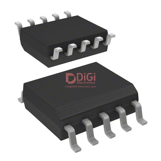
The VIPER06HSTR integrates advanced insulation capabilities through its 10-pin SSOP package, engineered for enhanced creepage distances. This design achieves a certified creepage for 800 V insulation, closely aligning with stringent IEC safety norms required in industrial power supply architectures. Manufacturing precision ensures that package boundaries maintain physical separation between high-voltage and low-voltage pins, optimizing the device for safety-critical applications such as isolated flyback converters and auxiliary power units.
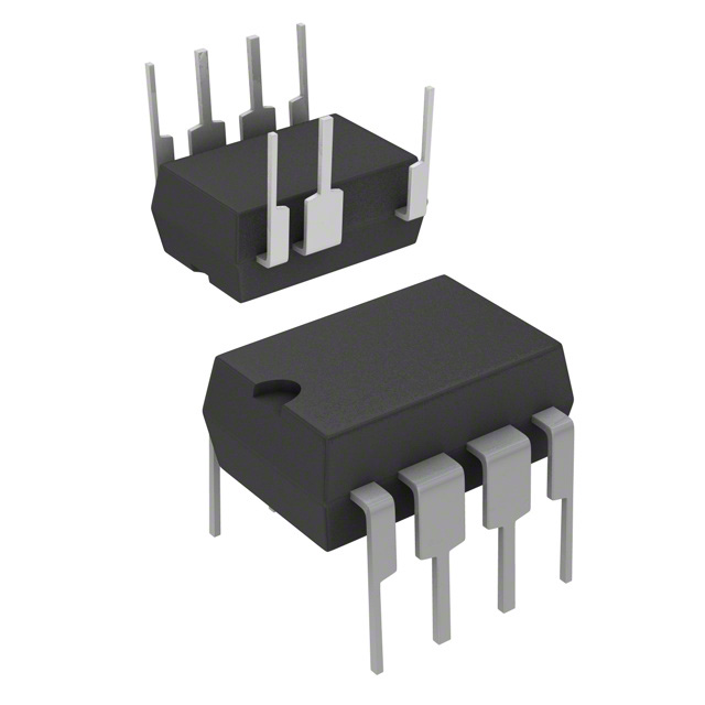
In compliance management, STMicroelectronics applies ECOPACK® protocols, embedding RoHS-compliant materials and process flows to minimize hazardous substance presence. This approach streamlines integration into green electronics supply networks, supporting assembly lines where regulatory scrutiny and lifecycle impact assessments are persistent concerns. Package choice influences not only electrical isolation but also the reliability of surface mount processes; the SSOP variant exhibits low profile geometry, reducing solder joint stress during reflow, while the DIP-7 alternative, detailed in comprehensive mechanical drawings, offers ease of prototyping and dual-insertion compatibility for hybrid assembly tracks.
Technical documentation provides granular package outlines, essential for CAD library generation and IPC-compliant footprint fabrication. This precision in dimensional data minimizes assembly defects, yielding consistent solder quality across high-volume production. Close attention to package pad layout—especially regarding pin spacing and copper clearances—proves critical where electrical isolation and automated optical inspection thresholds converge. Practical deployment often necessitates revalidation of assembly ovens and stencil configurations based on specific package recommendations, an area that consistently emerges as a key determinant of first-pass yield rates.
Notably, long-term field returns indicate lower failure incidence when design teams incorporate the provided creepage specifications from initial PCB layout stages, rather than relying on post-production modifications. Package-environment interactions, such as moisture sensitivity and flux compatibility, further influence downstream reliability, especially in environments with tighter environmental compliance audits. Prioritizing standardized insulation and environmental protocols at the component selection phase reduces risk exposure and facilitates seamless certification, imparting a measurable advantage in regulatory-driven markets.
Potential equivalent/replacement models for VIPER06HSTR
In the search for suitable replacements or equivalents to the VIPER06HSTR, engineering analysis prioritizes alignment with circuit demands and operational constraints. STMicroelectronics provides a spectrum within the VIPER06 family, including the VIPER06Xx (optimized for 30 kHz operation) and VIPER06Lx (targeted at 60 kHz), each addressing specific switching frequency requirements and thus serving diverse efficiency or electromagnetic compatibility (EMC) objectives. These variants feature integrated MOSFETs and robust PWM control, fostering straightforward design-in for low- to medium-power offline converter topologies.
Selection parameters extend beyond frequency, encompassing breakdown voltage—typically in the 700V range for universal mains compatibility—along with standby power, where the VIPer™ series consolidates its position through milliwatt-level idle consumption. Engineers often utilize such properties to meet regulatory requirements for no-load and light-load efficiency, notably in consumer and industrial power supplies. Package formats, such as SO-8 or DIP-7, also influence the interchangeability, with mechanical constraints dictating layout reuse and minimizing redesign risk.
Exploration of alternatives must also consider competitive offerings from vendors like ON Semiconductor, Infineon, or Power Integrations, each providing high-voltage PWM controller ICs with similar architecture—integrated switches, advanced fault protection (over-temperature, overload, VDD undervoltage lockout), and soft-start mechanisms to mitigate stress during startup. Beyond datasheet values, practical deployment reveals nuanced distinctions: some devices exhibit improved startup time for rapid power-up, or enhanced latch-off protocols delivering greater reliability in fault-heavy environments.
From iterative prototyping to field deployment, confidence in replacements rests on thorough validation under full-range input line conditions, loading scenarios, and abnormal operation. Significant experience demonstrates that datasheet equivalency, while necessary, rarely suffices for direct drop-in substitution—parameters like dynamic response to load transients, EMI profiles under switching edges, and thermal performance often vary. Strategic evaluation incorporating bench testing, thermal imaging, and real-world stress cases typically uncovers subtle but crucial differences in efficiency and robustness.
Emerging trends indicate that tighter integration and more intelligent fault-handling mechanisms are shaping the next generation of PWM switchers. Devices with higher breakdown voltage margins and further reduced standby power hold strategic advantage for applications facing stricter efficiency standards. Insightful selection thus combines specification-centric analysis with empirical vetting, harmonizing electrical, mechanical, and system-level criteria for optimal converter performance and lifecycle reliability.
Conclusion
The VIPER06HSTR from STMicroelectronics exemplifies the convergence of advanced integration and efficiency in modern offline switch-mode power supply design. By embedding a high-voltage power MOSFET with a proprietary control IC in a compact package, the device achieves a significant reduction in external components. This integrated approach streamlines both the schematic complexity and the physical layout, mitigating sources of EMI while enhancing reliability. The internal MOSFET is optimized for fast, low-loss switching, supporting high energy conversion efficiency even under variable or light load conditions, a crucial factor in meeting strict standby power standards.
At the controller level, the device incorporates a suite of protections—overvoltage, overload, short-circuit, and thermal shutdown—each precisely coordinated to shield sensitive circuitry from abnormal events. These embedded features obviate the need for numerous external protection components, thus minimizing failure points and simplifying qualification for global safety compliance. The presence of a fixed frequency oscillator and a quasi-resonant operating mode strikes a balance between efficiency and simplicity, enabling tight output regulation without the overhead of complicated control schemes. Notably, the flexible configuration, with reprogrammable feedback and input options, accommodates a diversity of end-product requirements, from simple chargers to compact household appliances.
Implementing the VIPER06HSTR in real-world applications reveals its value in addressing both technical and logistical constraints. The reduced component count directly translates to lower assembly costs and improved manufacturability, critical in price-sensitive high-volume sectors. Thoughtful PCB layout, such as short, low-inductance traces for switching nodes and proper heat dissipation provisions, heightens both electromagnetic compatibility and long-term durability. Field deployments consistently demonstrate robust start-up behavior and quick response to load transients, factors that contribute to overall system stability in unpredictable operating environments.
Comprehensive integration, reinforced by adaptive protection mechanisms, positions the VIPER06HSTR as a pragmatic choice for designers seeking resilience without sacrificing efficiency. In power system architectures where board space, regulatory compliance, and rapid development cycles converge, leveraging such devices establishes a competitive edge. Selecting and deploying this platform paves the way for innovative form factors and streamlined supply chains, highlighting the compound benefits of modern power integration.