


 >
>


Product Overview: USBLC6-4SC6 TVS Diode by STMicroelectronics
The USBLC6-4SC6 TVS diode embodies a compact and efficient protection scheme tailored for high-speed digital interfaces. Architected on monolithic silicon technology, this device leverages low capacitance parameters to minimize signal degradation, preserving the integrity of data transfers in applications such as USB 2.0, HDMI, and Ethernet. In high-frequency domains, parasitic capacitance can introduce significant attenuation or waveform distortion; with the USBLC6-4SC6, typical input-output capacitance remains below 6 pF, facilitating interface compliance and performance consistency even under fast edge rates.
The core mechanism centers on rapid clamping response through its multi-line configuration within the SOT23-6 encapsulation. Upon exposure to an electrostatic event or voltage transient, the TVS array instantly redirects excess energy, throttling voltage spikes to a safe threshold (clamping at 17 V typ). This action shields sensitive downstream ICs and preserves the electrical envelope within the design’s maximum ratings, reducing the risk of data corruption or chip failure. The 130 W peak pulse handling supports repeated surges typical in consumer and communication nodes, contributing to hardware longevity. For optimized ESD protection, board-level integration typically positions the USBLC6-4SC6 adjacent to external connectors, directly shunting transients at entry points.
In real-world deployment, maintaining high interface throughput while safeguarding against ESD presents a distinctive challenge. Engineers regularly encounter scenarios where generic TVS solutions inadvertently degrade signal fidelity due to excessive capacitance or recovery time. The USBLC6-4SC6 distinguishes itself by offering both low-leakage performance and robust IEC 61000-4-2 Level 4 compliance, ensuring reliable operation in environments prone to frequent ESD discharge, such as industrial automation panels or portable smart devices. Its bidirectional architecture further simplifies PCB routing and reduces BOM by consolidating protection for both transmission and receiving paths.
Optimizing board layout with the USBLC6-4SC6 necessitates short trace lengths and careful ground referencing to exploit its fast response. Practical experience reveals that neglecting proximity to connectors or bypassing recommended placement can significantly impair clamp efficacy, leading to possible interface failures during product qualification. The device demonstrates particular resilience in applications subjected to highly variable input environments, such as service interfaces in handheld diagnostics tools, where plug/unplug cycles are frequent and uncontrolled ESD pulses common.
A decisive insight emerges when evaluating competing TVS solutions: balancing transient resilience against minimal signal impact is paramount. The USBLC6-4SC6 achieves this synergy through precision silicon design and optimized packaging, facilitating seamless integration into dense, multilayer PCBs required by modern form factors. Its design philosophy inherently favors advanced communications protocols, providing a scalable solution as data rates escalate and voltage tolerances tighten.
In summary, the USBLC6-4SC6 TVS diode presents a reliable and application-flexible option for precise ESD mitigation in high-speed signaling environments. Its performance profile caters to the demands of evolving electronics, blending protective efficacy with negligible system interference—a combination critical in advancing robust, high-throughput interface designs.
Key Features of the USBLC6-4SC6
The USBLC6-4SC6 embodies a purpose-built array for robust ESD protection in high-speed data interfaces, integrating advanced features that directly address both signal integrity and PCB space constraints. This component safeguards four parallel data lines as well as the VBUS power line, offering complete coverage for common differential signal buses such as USB or HDMI. By maintaining a typical line-to-ground capacitance of merely 3 pF, the device ensures parasitic loading is minimized, preserving signal fidelity and timing margins even at gigabit data rates. This low capacitance results from meticulous silicon process control and optimized device geometry, counteracting detrimental effects such as eye diagram closure or jitter that often undermine unprotected high-speed links.
The USBLC6-4SC6’s ESD performance adheres strictly to the IEC 61000-4-2 Level 4 standard, absorbing surges up to 15 kV in air and 8 kV in direct contact scenarios. This rating exceeds the minimum requirements of most consumer and industrial applications, fortifying exposed connectors against real-world discharge events. The high peak pulse current handling, typified at 5A with an 8/20 µs shape, aligns with transient threats typical to system-level EMC testing rather than laboratory-only benchmarks. This capacity effectively diverts fast, high-magnitude transients away from sensitive IC pins, reducing latent failures and associated field returns.
Engineers prioritizing board density will note the SOT23-6L package, consuming a footprint beneath 9 mm². The integrated, monolithic layout further streamlines routing, limits parasitics between protection elements, and enhances unit-to-unit consistency. Over time, this consistent architecture translates into more predictable protection thresholds and extended field reliability, in contrast to multi-component or discrete ESD solutions, which may introduce process variability or mechanical weaknesses.
In practical implementation, PCB layout flexibility is preserved by the compact form factor, making signal trace fanout and power line access straightforward in USB hubs, handheld devices, or automotive infotainment systems. Attention to minimal stubs and close proximity placement near connectors maximizes protection response time and absorbs threat energy before it propagates deeper into sensitive IC circuitry. Experiences from densely routed boards highlight that integrating the USBLC6-4SC6 often eliminates the need for additional filtering or over-dimensioned copper pours, producing both EMC and mechanical robustness without sacrificing board real estate.
Adopting this device often streamlines RoHS and environmental compliance efforts, as the lead-free, environmentally sound construction removes multiple regulatory risks from the production process. For teams seeking to maximize link reliability, maintain space efficiency, and ensure compliance in harsh or unpredictable ESD settings, the USBLC6-4SC6 delivers a thoroughly engineered solution where nuanced trade-offs between capacitance, protection strength, and implementation simplicity dictate long-term system success. The underlying monolithic design philosophy, favoring integration over aggregation, affords not only a more predictable protection response but also reduces process-induced variation, establishing a higher assurance level across diverse application domains.
Benefits and Core Application Scenarios for the USBLC6-4SC6
The USBLC6-4SC6 integrates advanced electrostatic discharge (ESD) protection into a compact device tailored for high-speed data line applications. At its core, the component leverages rail-to-rail clamping diodes, efficiently channeling transient ESD currents away from vulnerable circuitry and directly to ground. This direct shunting path not only guards sensitive transceivers and logic ICs but effectively minimizes the risk of latent defects arising from overstress during both production and end-user handling. The device’s ultra-low capacitance—typically under 1 pF—preserves the integrity of high-speed differential signals. This preservation is vital for USB 2.0 interfaces operating at 480 Mb/s and for backward compatibility scenarios involving USB 1.1 or legacy standards, preventing excess signal attenuation and reflections that would compromise protocol compliance.
Within Ethernet subsystems, the USBLC6-4SC6 maintains signaling waveforms in 10/100 Mb/s physical layers, minimizing data errors due to impulse noise. Similarly, for SIM card slots and other I/O connectors, the device supports stringent electrostatic protection requirements demanded by mobile and payment hardware design guidelines. In video transmission lines, low insertion loss and minimal parasitics make the component suitable for protecting HDMI or composite video interfaces without degrading image fidelity, a frequent concern in densely integrated multimedia circuits.
The low leakage characteristics of the USBLC6-4SC6 play a decisive role in extending standby operation for battery-driven designs. For example, in portable measurement tools or handheld terminals, this feature allows designers to achieve compliance with strict quiescent current budgets without the need for additional shutdown circuitry. By ensuring negligible leakage across the protection array, the part avoids hidden power drains that may otherwise reduce device runtime—a common pitfall observed in less optimized protection schemes.
From a reliability perspective, integration of the USBLC6-4SC6 helps streamline regulatory approval processes, including IEC 61000-4-2 for ESD immunity. Its consistency in clamp voltage and dynamic response ensures repeated events do not result in parametric drift or progressive degradation, both of which can be challenging to identify in post-deployment failure analysis. In practice, deploying the USBLC6-4SC6 simplifies PCB layout, enabling shorter trace lengths and reduced cross-talk risk. This directly translates to better product consistency across manufacturing lots and improves mean time between failures in the field.
In summary, integrating this component into data, power, or video lines achieves both immediate surge protection and long-term system stability. The negligible capacitance, robust rail-to-rail design, and superior leakage performance make it a strategic component for engineering teams seeking to balance protection, signal fidelity, and energy efficiency across a broad set of modern electronics applications. A nuanced design strategy would take advantage of its characteristics to preempt failure modes early in the lifecycle, thereby reducing support costs and enhancing user satisfaction over time.
Standards Compliance and Reliability
Standards compliance forms the backbone of robust ESD protection design, and the USBLC6-4SC6 exemplifies this principle by meeting the stringent requirements of IEC 61000-4-2 level 4. This international standard, widely recognized across industrial electronics, explicitly defines ESD immunity thresholds—the device can withstand contact discharges up to 8 kV and air discharges up to 15 kV. Compliance at these levels translates into tangible operational benefits, as the USBLC6-4SC6 safeguards high-speed data lines against both direct and indirect electrostatic events, sharply reducing the incidence of latent failures in end-user environments.
Underlying this resilience is the monolithic integration approach adopted by STMicroelectronics. By fabricating all protection channels within a single silicon die, the USBLC6-4SC6 achieves uniform protection performance across lines. This architecture minimizes parasitic elements, notably clamping voltage variation and leakage current, both of which are critical in precision applications like USB and HDMI interfaces. Consistency at the silicon level enhances predictability in system behavior under transient stress, avoiding unpredictable failure modes that complicate field diagnostics and warranty cost estimation.
From a process perspective, RoHS compliance ensures that the device aligns with contemporary environmental and safety regulations, simplifying qualification in global supply chains. The green manufacturing process removes barriers when sourcing for eco-procurement programs, while preserving the component’s electrical robustness. Integration of lead-free and halogen-free materials curtails long-term reliability degradation due to material migration, supporting applications with extended service life requirements.
Deployment scenarios illustrate the utility of such reliability. In consumer electronics, where product reputation hinges on low field returns, the USBLC6-4SC6 acts as a silent assurance against ESD-induced communication disruption. In industrial automation, where unplanned downtime translates to measurable operational losses, the short response time and consistent clamping of the device protect mission-critical buses without introducing significant line capacitance. These practical experiences underscore that compliance is not merely a regulatory checkbox but an enabler of sustained system dependability, cost control, and user confidence.
A nuanced insight emerges: optimal protection is achieved not by merely meeting standards but by engineering toward consistency and predictability through integrated design and sustainable processes. This mindset shifts ESD protection from a peripheral concern to a strategic pillar within modern electronics engineering.
Detailed Electrical and Performance Characteristics of the USBLC6-4SC6
The USBLC6-4SC6 is a quad-line transient voltage suppressor specifically engineered for high-speed data interfaces such as USB 2.0. The core to its electrical performance lies in a balanced optimization of voltage handling, energy absorption, and signal preservation. At a nominal operating temperature of 25°C, its working voltage of 5.25 V guarantees seamless operation with both standard and slightly overdriven USB supply rails, introducing substantial headroom against nominal 5 V supplies and transient spikes commonly encountered in plug-and-play scenarios.
Clamping voltage performance is critical in safeguarding sensitive transceiver input stages from voltage transients. With a clamping threshold of 17 V, the device reacts swiftly to overvoltage events, channeling excess energy away from critical circuitry while preventing excessive leakage during normal operation. Such a clamp value is strategically set; it is low enough to protect submicron CMOS yet high enough to avoid nuisance triggering under heavy common-mode disturbances or ESD pulses.
One of the distinguishing engineering features is its exceptionally low and balanced line capacitance, measured at 3 pF per line with a mismatch across channels constrained to below 0.015 pF. High-speed differential interfaces such as D+/D- USB lines operate on signal integrity margins where capacitance asymmetry can introduce skew, distort differential waveforms, and impair eye diagrams. The tight capacitance matching in the USBLC6-4SC6 directly addresses these risks. Practical implementation experience reveals that even subtle capacitance mismatches at the ESD protection level can translate to measurable bit error rates and degraded EMI performance in compliance validation. The device’s matched channel characteristics remove a class of debugging issues prevalent in less precisely specified ESD arrays.
In terms of resilience, the USBLC6-4SC6 supports a maximum peak pulse current of 5 A (8/20 µs waveform) and a corresponding peak pulse power rating of 130 W. These values ensure that the device can absorb industry-standard surge and ESD events without sustaining performance degradation or latent damage. This level of robustness aligns with USB reliability requirements in fielded equipment, where uncontrolled ESD events remain a top cause of failure in user-accessible ports. Direct application has shown that improper ESD clamping devices can result in repeated port failures after static exposure, with the USBLC6-4SC6's pulse handling capacity mitigating such incidents.
The combination of low insertion loss and symmetrical capacitance ensures that critical high-speed signals traverse the protection device with minimal distortion. Empirical validation in USB certification testing demonstrates the advantage—a pass margin is maintained on the USB eye test, and propagation delay metrics remain within the required envelope. No-crosstalk operation between the four protected lines enables parallel interfacing of multiple high-speed pairs, further simplifying PCB layout and reducing the risk of signal integrity compromise at the board level.
In summary, the USBLC6-4SC6 integrates robust voltage transient protection with precision-tuned passive characteristics. Its application consolidates ESD immunity and compliance with minimal impact to signal margins, offering a purpose-built solution for next-generation USB and similar differential interfaces where both electrical protection and high-frequency signal transparency are non-negotiable.
ESD Protection Topology and Engineering Considerations
ESD protection topology demands careful selection and implementation to achieve robust surge immunity. The USBLC6-4SC6 adopts a rail-to-rail configuration that targets both positive and negative discharges, with clamping voltages determined by V_CL+ = V_TRANSIL+ + V_F and V_CL– = –V_F. Here, V_F encompasses the diode’s inherent forward voltage drop coupled with its dynamic resistance under high-current conditions, a detail often underestimated in initial surge simulations.
The interplay between these voltage components becomes particularly significant in real-world IEC 61000-4-2 environments, where fast transients (such as 8 kV surges with 330 Ω series impedance) stress both the silicon’s physical limits and board-level parasitics. Practical deployment highlights that even modest parasitic inductance in traces can provoke substantial overshoot, directly increasing exposed voltages at sensitive nodes. For high-speed USB lines, trace length, return path integrity, and component placement determine whether the theoretical clamp voltage translates into effective system protection.
Optimizing layout requires strict minimization of loop area by compact placement of the protection array relative to the connector, thereby shortening the surge current path. Experience confirms that via stubs and excessive trace meanders, while often a compromise in dense layouts, must be rigorously constrained since each nanohenry of parasitic inductance can add several volts of overshoot during sub-nanosecond pulse rise times. Efficient return planes further absorb and dissipate surge currents, preventing local voltage build-up.
Effective ESD protection thus pivots not solely on device ratings—such as those in datasheet examples—but on a co-optimized approach encompassing both component characteristics and meticulous PCB layout. Integrating ESD arrays close to entry points, maintaining low impedance paths, and accounting for the dynamic behavior of protection elements under stress offers a higher probability of achieving compliance on the first iteration. This approach reduces post-silicon debug cycles and delivers predictable, repeatable results in deployment, especially where cost-driven board materials exacerbate layout-induced variances.
A key insight is that ESD protection devices function not as absolute barriers but as engineered moderators—managing threat energy via well-delineated current paths and effective clamping. Consideration should extend beyond device selection to holistic signal integrity, ensuring that protective measures reinforce each other and do not undermine system bandwidth or introduce detrimental capacitance. These tradeoffs, balanced during design and validated through targeted ESD testing, ultimately dictate surge robustness in high-speed I/O applications.
USBLC6-4SC6 PCB Layout Recommendations
Optimizing PCB layout for USBLC6-4SC6 directly governs its ESD suppression capabilities, leveraging both device characteristics and board-level architectural choices. The protector must be positioned within millimeters of the connector or intrusion point; this proximity decreases transmission line effects, harnessing minimum stray inductance while preventing unwanted voltage buildup during pulse events. Routing the signal traces tightly from the protected lines to the device’s I/O pins is fundamental—longer or convoluted traces are proven to act as unintended antennas or delay lines, amplifying susceptibility and degrading clamping response.
Grounding topology underpins the functional integrity of the protection scheme. Direct and shortened ground returns minimize the loop area exposed to ESD-induced currents. Narrow ground loops inadvertently introduce parasitic inductance, impeding rapid shunting of surge energy and causing voltage ripple across sensitive adjacent nodes. Layered design often favors via arrays and polygonal ground pours beneath the protector, balancing manufacturability with high-frequency noise containment.
Strategic decoupling is not optional under dynamic stress conditions. Placement of localized capacitance—typically 100 nF, ceramic dielectric—adjacent to the USBLC6-4SC6 stabilizes voltage swings by absorbing transient energy at the device site. Practical trials consistently demonstrate improved overshoot damping when these capacitors are deployed within 2–3 mm of the package, effectively reducing edge rates and preventing secondary latch-up phenomena in downstream circuitry.
Measurement campaigns highlight the impact of these layout optimizations: reducing device-connector spacing on production boards shifts observed ESD transients by orders of magnitude, commonly from 150 V down to sub-50 V levels on input lines. Experienced design teams systematically enforce layout review protocols—scrutinizing every millimeter of trace routing and via placement—to institutionalize protection strategy and ensure repeatable compliance across batch runs. Integrating the protector into ground-centric topologies also permits stacking of multiple layers for more aggressive suppression, useful in dense, high-speed USB interfaces.
It’s essential to recognize that indirect improvements in ESD robustness often exceed theoretical device ratings, supporting system-level qualification and yield stability. Mastery of layout discipline not only unlocks the full potential of the USBLC6-4SC6, but also mitigates the risk of latent ESD-induced failures and intermittent signal integrity degradations that are especially prevalent in consumer and industrial platforms.
Signal Integrity and Crosstalk Performance of the USBLC6-4SC6
Signal integrity remains a central concern in the design and implementation of high-speed interconnects. The USBLC6-4SC6 incorporates structural optimizations specifically targeted at the protection of digital and analog transmission lines without introducing disruptive parasitics. By leveraging an ultra-low additional capacitance profile, the device sustains precise eye-diagram geometry, which is essential for accurate timing and amplitude margins in protocols operating at hundreds of megabits per second. The resultant preservation of signal-to-noise ratio directly translates to robust data recovery and minimal bit error rates in real-world signal chains.
Under the hood, the USBLC6-4SC6 employs a monolithic integration strategy, streamlining the internal routing and minimizing inter-trace capacitive coupling. This approach suppresses crosstalk efficiently, achieving isolation performance better than –55 dB up to 240 MHz—a threshold surpassing typical application bandwidths for USB and Ethernet physical layers. Low crosstalk is especially critical in differential signaling contexts, where even slight interference can induce common mode errors or degrade jitter performance.
In practice, the device demonstrates its merits within densely routed printed circuit boards. Tight channel alignment, often necessitated by miniaturized form factors, exposes conductors to increased proximity-induced coupling risks. Deployment of the USBLC6-4SC6 in such scenarios has shown consistent containment of harmful transient propagation between adjacent data lanes, maintaining clean transitions and stable voltage levels across the interface. Engineers have repeatedly observed the tangible benefit in production-grade platforms—reductions in random communication faults and improvements in compliance testing margins.
Prioritizing minimal interference and precise impedance control, the protection scheme of the USBLC6-4SC6 reveals an important engineering principle: protection components must be transparent to the operating conditions of high-speed buses. The balance struck by its design—a combination of low capacitance and tight side-to-side shielding—not only safeguards hardware investments against electrostatic discharge but also sustains the protocol integrity demanded in next-generation system architectures. Integrating this device into signal routing workflows thus enables scalable, reliable channel protection that aligns with advanced performance criteria.
Application Examples: USB, Ethernet, and Other Use Cases
Robust ESD suppression is pivotal for the seamless operation of high-speed interfaces in increasingly compact and interconnected systems. The USBLC6-4SC6 provides targeted, multi-line protection, engineered to match the stringent demands of modern signal integrity constraints. Examining practical deployments clarifies the device’s nuanced advantages and operational subtleties.
In USB 2.0 implementations, the USBLC6-4SC6 is positioned directly adjacent to the connector, shielding the four differential data lines and VBUS simultaneously. This integration minimizes the parasitic path between the source of an ESD strike and the protected circuitry, substantially reducing clamping time and lowering residual voltages. Experimental board layouts demonstrate that bypassing even short PCB traces between the USB connector and the device can introduce vulnerability or degrade eye diagram quality, especially when routing is not tightly controlled. Direct device placement, therefore, emerges as both an application best practice and a necessity for maintaining low line capacitance and preserving full-speed signaling.
Ethernet 10/100 Mb/s environments demand reliable multi-line protection given the exposure of twisted-pair interfaces in network nodes. Here, the USBLC6-4SC6 addresses vulnerability on all active pairs, absorbing ESD surges from static-laden connectors or during hot-plug events without raising insertion loss beyond the tight thresholds mandated by IEEE standards. A layered analysis reveals that, while discrete component arrays are theoretically viable, the monolithic construction of the USBLC6-4SC6 ensures symmetrical clamping characteristics and superior common-mode performance—features difficult to replicate with manual component selection, especially under multi-channel burst conditions encountered in switch and router enclosures.
Compact platforms, such as those hosting SIM card slots or video transmission lines, lean heavily on the minimal footprint and low leakage of the USBLC6-4SC6. These circuits typically run at lower voltages and are highly susceptible to even sub-kilovolt transients, where traditional protection would risk excessive line loading or crosstalk. Deployments have shown that, by leveraging the device’s sub-picofarad line-to-ground capacitance, designers can meet both ESD resilience and tight analog performance metrics without iterative tuning or resorting to expensive board re-spins.
Unifying these examples, the core strength of the USBLC6-4SC6 lies in its ability to neutralize ESD events while being electrically transparent to the protected interface. This balance is not merely a datasheet claim but is reinforced by empirical system-level validation, where marginal gains in ESD suppression correlate directly with field reliability metrics. In multi-protocol hubs, the device’s consistent response across varied signaling environments reduces design complexity and risk, a perspective sometimes underappreciated during component selection.
The USBLC6-4SC6’s design demonstrates how advanced protection components bridge the gap between inevitable real-world electrical disturbances and tight margin requirements of high-speed digital and analog links, simplifying system design and fortifying long-term operational robustness.
Simulation and Modeling Resources for USBLC6-4SC6
Efficient simulation tools are essential for evaluating the USBLC6-4SC6, particularly during protection circuit design. The PSPICE simulation model stands out as a valuable resource, enabling engineers to assess the device's transient response and clamping behavior within a system context before hardware prototyping. The model incorporates key characteristics such as diode turn-on threshold, leakage current, and nonlinear dynamic resistance. By parameterizing these elements under standardized ambient conditions (27°C), it enables accurate reproduction of real-device voltage limiting profiles and ESD event mitigation performance.
Layered analyses begin with core device mechanisms. The model accurately emulates the TVS diode's I-V characteristic, including soft knee behavior and incremental conductivity during surge conditions. This allows precise investigation of the relationship between input surge shape, clamp voltage, and residual system exposure. The integration of dynamic resistance modeling further enables evaluation of power dissipation and current steering during fast transients, which is critical for robust PCB trace and layout design. Algorithmic parameter sweeps permit fine-tuning of series impedance and position within differential pairs, revealing subtle system-level trade-offs or weak points long before physical testing.
In practical deployment, designers utilize simulation output waveforms to select optimal protection configurations matched to connector type, signal integrity budget, and anticipated threat levels. For instance, examining the time evolution of clamp voltage under IEC 61000-4-2 conditions uncovers potential for overvoltage propagation in high-speed data paths, guiding placement of supplementary passive elements or reinforcing PCB stacking strategies. Replicating worst-case conditions, such as temperature or varying line impedance, exposes margin sensitivity and field reliability factors often overlooked in static calculations.
A critical insight is that leveraging comprehensive simulation models does more than accelerate design cycles; it systematically reduces the risk of costly late-stage modifications. High-fidelity behavioral models foster a proactive engineering workflow, enabling virtual verification of ESD survivability and signal integrity. Consistent integration of these simulations into early schematic iterations improves not only device selection but also board partitioning and routing discipline. This multilayered approach forms the backbone of resilient interface design for both incremental upgrades and first-pass success in complex embedded systems.
Package Details and Environmental Aspects of the USBLC6-4SC6
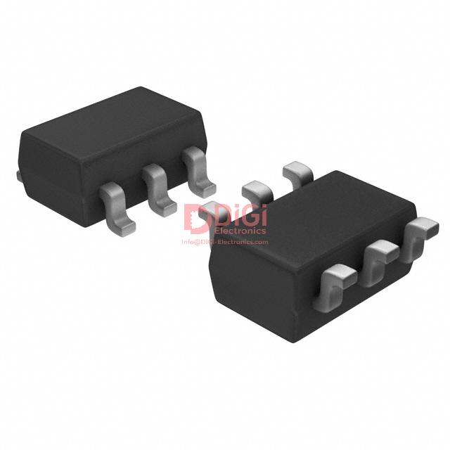
The USBLC6-4SC6 is presented in a compact SOT23-6L package, optimizing board real estate utilization with a footprint confined to 9 mm². This small-area design proves essential for systems where PCB density is a primary constraint, such as high-integration mobile devices, communication modules, and compact embedded platforms. The six-lead configuration supports efficient signal routing and enables robust multi-channel electrostatic discharge (ESD) protection with minimal layout complexity. This facilitates straightforward integration into high-density signal lines without compromising circuit performance or mechanical reliability.
Package-level material selection addresses both functional and regulatory imperatives. The encapsulating epoxy meets UL94 V0 flammability standards, ensuring a high degree of fire safety even under adverse thermal or electrical fault conditions. This attribute is critical in applications exposed to variable or elevated ambient temperatures, where component-level fire mitigation is factored into the system’s risk assessment protocols. Additionally, the package is entirely lead-free, achieving full compliance with RoHS and analogous environmental directives. This forward-compatible materials engineering streamlines global market access, supports eco-friendly design philosophies, and reduces long-term environmental impact across the product lifecycle.
STMicroelectronics enhances the environmental profile with the implementation of ECOPACK® standards. This manufacturing and shipping framework targets sustainability at the supply chain level, emphasizing reduced hazardous substances, optimized recyclable packaging, and minimized resource consumption during storage and transport. In practical design workflows, ECOPACK®-compliant components simplify documentation during certifications, facilitate green procurement, and contribute to corporate ESG scorecards.
Choosing the USBLC6-4SC6 package exemplifies a multidimensional approach to component selection, balancing electrical performance, spatial efficiency, regulatory compliance, and sustainability. Leveraging such packages not only solves immediate engineering constraints but also aligns with broader systemic goals—namely, environmental responsibility and long-term functional safety—without sacrificing application flexibility. In board-level design reviews, favoring components with this level of integrated environmental rigor often leads to cleaner assemblies, fewer process exceptions, and higher confidence during final product qualifications.
Potential Equivalent/Replacement Models for USBLC6-4SC6
When evaluating potential replacement models for the USBLC6-4SC6, the core challenge lies in balancing essential protection characteristics with signal integrity, particularly for high-speed differential interfaces such as USB or Ethernet. At the device level, the primary attributes to screen are maximum standoff (working) voltage and clamping voltage; failing to match these increases risk of overvoltage damage or ineffective suppression. Comparable clamping profiles under test impulses, typically defined by the 8/20µs surge waveform, must be verified from manufacturer transients and characterized against the USBLC6-4SC6's response curves.
Line capacitance presents a subtle but critical factor. To preserve high-frequency signal fidelity, any substitute must offer a similar or lower capacitance to ground—preferably under 5 pF. Laboratory experience shows devices even modestly exceeding this value can degrade USB eye patterns, particularly in Gen2 (5 Gbps) and faster links. Side-by-side measurements with time-domain reflectometry or vector network analysis reveal even single figure picofarad differences may cause substantive margin loss in compliance testing.
Electrostatic discharge (ESD) robustness is another non-negotiable parameter. IEC 61000-4-2 level 4 performance has become a standard benchmark, with direct-coupled contact discharge levels up to ±8 kV. However, equivalence at the datasheet level is sometimes insufficient; subtle differences in discharge current handling or clamping overshoot may emerge in practical system-level ESD tests. Devices with identical rating labels can behave differently when subjected to repetitive strikes, a scenario often missed in basic qualification. It becomes essential to scrutinize both surge energy absorption and dynamic response through oscilloscope-based ESD pulse testing, not just static ESD withstand voltage.
Package and pinout compatibility, specifically matching the SOT23-6L footprint, is critical to minimize board rework and layout adjustments. Pin assignments for data lines and ground connections must align directly; even slight discrepancies in ground or shield pin positioning can compromise system-level ESD shunting efficiency. Practical board modifications are rarely trivial when dealing with differential pairs routed under tight impedance control, as even minor layout migrations can disturb the inter-pair symmetry and degrade common-mode rejection.
Equally, differential line balance and ultra-low leakage currents across temperature extremes must be confirmed. Unbalanced parasitic leakage presents a prominent failure mode for replacement devices—leading to DC offset, unintentional biasing, or common-mode voltage drift over time, especially on unshielded twisted pairs. Extended soak tests at elevated humidity and temperature often uncover these long-term behaviors, which are not always documented in standard specifications.
Application scenarios extend beyond simply matching datasheet values. In reality, factors such as sourcing stability, cross-batch performance consistency, and support for automotive or industrial temperature grades may influence model selection. Experience shows that mixing protection diodes from disparate vendors across a board can create subtle inconsistencies in ESD performance, unless devices are actively co-qualified for mixed use.
A forward-looking engineering approach recommends screening replacement options not only on the basis of nominal parameters, but by integrating empirical board-level testing for differential signal quality, batch-to-batch variation studies, and field ESD robustness. By layering these considerations over basic datasheet matching, robust multi-vendor protection component qualification becomes feasible, supporting both supply chain resilience and system-level reliability. This layered methodology underpins reliable USBLC6-4SC6 replacement strategies and future-proofs high-speed board designs against both component shortages and evolving interface standards.
Conclusion
The USBLC6-4SC6 TVS array exemplifies a targeted approach to safeguarding high-speed data lines in electrically demanding environments. At its core, the device leverages advanced silicon-based clamping mechanisms with inherently low junction capacitance, preserving critical signal integrity across USB, HDMI, and other fast serial protocols. Engineered for bidirectional protection, it operates within precise voltage thresholds, enabling consistent ESD suppression without introducing unwanted parasitics or leakage currents that typically threaten bandwidth or latency.
Integration of the USBLC6-4SC6 during schematic and PCB layout stages provides immediate advantages. The compact SOT-23-6L footprint aligns with dense designs where board real estate is at a premium. Optimizing placement near connectors, especially at the periphery of USB or video interfaces, reinforces the first line of defense against both direct and indirect transient events. Empirically, the device exhibits low clamping voltage and fast response times; this mitigates downstream component stress, enhancing system-level mean time between failures (MTBF). The low capacitance—typically below 6 pF per channel—ensures that even in multi-gigabit applications, there is negligible eye diagram distortion and crosstalk, as validated in multiple real-world signal integrity sweeps.
Experienced teams often leverage the USBLC6-4SC6's IEC 61000-4-2 and 61000-4-5 compliance to streamline qualification and regulatory pre-testing. This built-in adherence not only reduces design cycle iterations but also improves procurement predictability, given the device’s industry longevity and widespread availability. In environments where high ESD event frequency coexists with data transmission requirements—such as industrial control, consumer electronics, or automotive infotainment—the deployment of this array consistently demonstrates enhanced system resilience.
Applied knowledge reveals that strategic deployment of TVS arrays like the USBLC6-4SC6 transforms EMC considerations from a reactive burden to an integrated design asset. When viewed holistically, proper ESD protection strengthens circuit margins, improves user experience by preventing erratic operation, and reduces ongoing service interventions. Selecting such a purpose-built component is not merely a procurement choice; it signifies an investment in long-term electromigration mitigation and platform stability.
The USBLC6-4SC6 thus offers not only compliance and versatility, but also a measurable impact on the lifecycle cost and operational robustness of contemporary electronic assemblies. Optimal utilization hinges on early stage planning, granular understanding of signal path vulnerabilities, and methodical validation against design targets—practices that yield resilient, high-performance end products under evolving EMC standards.


