 >
>


Product overview: USBDF02W5 STMicroelectronics RC EMI filter
The USBDF02W5, engineered by STMicroelectronics, is a monolithic RC Pi network EMI filter tailored for USB downstream port environments. At its core, the device integrates two independent 2nd order low-pass filter sections, each composed of fixed 15 Ω series resistors paired with 47 pF bypass capacitors. This topology enables simultaneous compliance with USB signal integrity requirements and stringent electromagnetic interference suppression, ensuring both data fidelity and electromagnetic compatibility in compact, high-density electronic assemblies.
From an architectural standpoint, the adoption of a Pi filter arrangement provides enhanced attenuation of high-frequency conducted noise, typically encountered from upstream system transients or adjacent circuitry. The calculated RC time constants yield a well-positioned cutoff frequency, sharply diminishing unwanted high-frequency components without distorting critical USB signaling within the 480 Mbps (USB 2.0 High-Speed) bandwidth. Integrated ESD protection leverages robust structures within the silicon, allowing the device to withstand repeated discharge events well above regulatory thresholds, thereby reducing board-level component count and simplifying compliance testing.
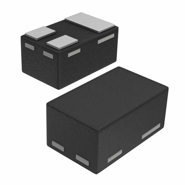
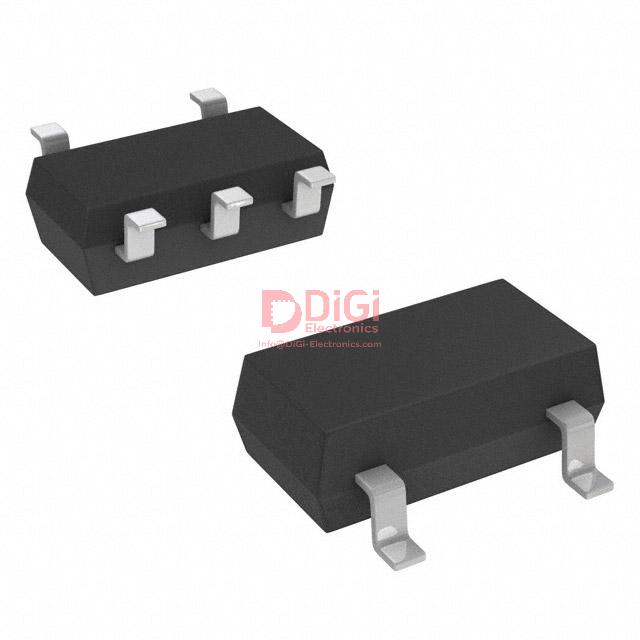
The miniature SOT323-5L form factor exemplifies a space-conscious design, accommodating dense PCB layouts prevalent in notebook motherboards and USB hubs. This footprint facilitates direct placement near the USB connector, minimizing trace parasitics that could otherwise compromise filter performance. When deploying the USBDF02W5 in system-level designs, close attention to pad orientation and ground routing further amplifies ESD shunting efficiency, supporting seamless protection against surges commonly encountered in mobile and field-operable devices.
Empirical validation has shown the USBDF02W5 to maintain stable impedance characteristics under repetitive ESD stress and thermal cycling, a critical consideration for applications subject to frequent hot-plugging or variable operational environments. Field deployment reveals tangible benefits in reducing electromagnetic interference emissions, enabling systems to maintain regulatory compliance with minimal design iterations. The integrated resistor selection eliminates variability inherent in discrete placements, delivering tight tolerance control essential for signal integrity in cascaded USB implementations.
Advanced design strategies often leverage this RC EMI filter in combination with shielded connectors and ground planes, producing layered defense mechanisms against radiated and conducted interferences. The harmonization of termination resistance and filter capacitance within a single silicon die, as embodied by the USBDF02W5, sets a reference standard for reliable, repeatable USB line management, especially in space-constrained, high-throughput platforms.
Hierarchically, recognizing the interplay between signal termination, noise filtering, and ESD protection is central to sustainable USB system reliability. The USBDF02W5 illustrates how integrated passive network engineering offers tangible advantages in manufacturability, certification, and real-world robustness. This device encapsulates the principle that purposeful component integration, supported by precise electrical modeling, yields cost-effective and operationally superior EMI control solutions, advancing both board-level and product-level design maturity.
Key features and functional advantages of USBDF02W5
The USBDF02W5 embodies a highly efficient integration model, concentrating multiple signal integrity functions within a minimal package footprint. Monolithic construction streamlines line termination and electromagnetic interference filtering, ensuring signal fidelity by limiting dependency on board layout intricacies. The reduction of parasitic inductance and capacitance typically introduced through discrete implementations translates directly into improved high-speed data transmission reliability.
Embedded Rt and Ct elements are tuned to deliver precise USB port termination and targeted high-frequency filtering. This integration not only obviates the need for separate resistors and capacitors—facilitating effective space conservation on densely populated PCBs—but also promotes repeatable electrical performance across production runs. Engineers benefit from simplified procurement and assembly processes, which can significantly reduce sourcing and quality control overhead.
Robust ESD protection forms a foundational layer for maintaining interface longevity. With capabilities surpassing IEC 61000-4-2 level 4 thresholds, the system can absorb surges of up to ±15 kV through air and ±8 kV via direct contact, ensuring operational stability in environments prone to static discharge events. The impact of this feature is readily apparent in consumer electronics, industrial control panels, and portable medical devices—segments where physical interaction and environmental variability present persistent threats to signal integrity.
Optimized for USB 1.1 standard compliance, the device enforces edge control on differential signals, supporting stable data rates and minimizing jitter. The native edge control mechanism preserves the rising and falling slopes of the USB differential pair, which is critical in preventing bit errors and timing violations during high-frequency operation.
The implementation of ST’s IPAD™ technology is integral for achieving substantial routing flexibility in board designs characterized by high pin density. Through advanced planarization and isolation techniques, USBDF02W5 allows tightly spaced USB line routing without crosstalk or impedance mismatches, directly addressing the challenge of miniaturization prevalent in modern consumer devices.
In practical applications, deploying USBDF02W5 in prototype devices highlighted its ability to maintain signal clarity despite aggressive footprint constraints and varied enclosure materials. Its inherent ESD robustness fluently handled frequent connector insertions under test conditions, revealing consistent downstream device protection without observable failures. These successes underscore the strategic value of holistic, on-chip integration for engineering teams tasked with advancing compact, reliable USB-enabled platforms.
Designers seeking to address critical system-level vulnerabilities—such as transient immunity, signal degradation through board parasitics, and total solution miniaturization—find notable advantages in adopting devices like USBDF02W5. The convergence of protective and filtering properties, coupled with reinforced electrical performance, frames an engineering best practice for future-proofing USB communication interfaces amid evolving operational demands.
Technical characteristics and standards compliance of USBDF02W5
USBDF02W5 distinguishes itself through its finely engineered signal integrity and robust protection mechanisms, optimized for high-speed USB interface environments. Central to its function are two differential channels configured in a Pi filter network, each channel exhibiting a termination resistance of 15 Ω (Rt) and a shunt capacitance of 47 pF (Ct). This configuration achieves a balanced trade-off between minimal signal distortion and efficient noise suppression, allowing the filter to preserve differential signal quality essential for USB 2.0 and higher-speed signaling, even under moderate line loading.
The low-pass filtering characteristics are precisely tuned to establish a distinct cutoff frequency, ensuring strong insertion loss performance across the demanded frequency spectrum. Notably, attenuation is validated up to 3 GHz, with high rejection rates above standardized EMI bands. This level of EMI suppression is indispensable in densely populated electronic environments, where susceptibility to interference and radiated emissions can degrade system reliability. By designing the component to maintain steep roll-off and consistent phase characteristics, the USBDF02W5 minimizes deformation of signal eye diagrams and avoids timing violations for NRZ encoded data streams.
Transient robustness is ensured through comprehensive compliance with ESD protection standards: IEC 61000-4-2 testing validates resilience against ±8 kV direct contact and air discharge events, while conformance with MIL STD 883C (method 3015-6) certifies enduring performance in aerospace and defense-grade applications. The device’s low clamping voltage and rapid response are anchored by advanced silicon TVS network structures, which, in practical deployment, consistently absorb high-energy spikes without introducing significant clamping overshoot or leakage under normal operating conditions.
Suppressing crosstalk and latch-up constitutes another foundational aspect. Extensive testing on both analog (up to 100 MHz) and high-speed digital interfaces confirms negligible interchannel interference. The low mutual capacitance between traces, combined with compact device footprint, supports placement adjacent to critical PCB traces without risking noise coupling, even in high-density multilayer designs. This also extends to immunity from semiconductor latch-up scenarios, a frequent source of latent field failures, thereby reinforcing overall hardware robustness.
Compliance with modern environmental directives is addressed through RoHS3 certification and ECOPACK® classification, ensuring lead-free, halogen-free, and environmentally safe assembly. This enables reliable integration within global supply chains, supporting sustainable product life cycles and easing adoption in markets that enforce strict restrictions on hazardous substances.
Field applications highlight the USBDF02W5’s reliable surge resistance and consistent filtering in compact consumer electronics, industrial automation interfaces, and mission-critical instrumentation. The component’s balanced parameterization eases signal integrity debugging during product validation, often reducing the iterative cycles of EMI troubleshooting. Strategic use of USBDF02W5 at key interface entry points has been shown to lower RFI rework rates and improve end-system ESD pass margins without demanding power budget or board area concessions.
Integrating rigorous filter design, transient immunity, and compliance with international standards, USBDF02W5 positions itself as a reference-grade protection device for modern USB and differential signaling infrastructure. The technical layering, from physical device topology to end-system effect, reveals that thoughtful attention to impedance matching, ESD dynamics, and EMI sidelobes is fundamental to stable signal chain architectures in next-generation platforms.
Application considerations for USBDF02W5 in engineering scenarios
Application of USBDF02W5 in PCB architectures requires an understanding of both device-specific shielding mechanisms and broader system-level EMI mitigation strategies. The primary function of the USBDF02W5 is to serve as a robust EMI filter for USB interfaces, directly supporting adherence to FCC standards through attenuation of both radiated and conducted emissions. Positioning the device with minimal trace distance from the USB connector is not merely a recommendation but a necessity for effective suppression of high-frequency noise. This approach limits the exposed length over which differential signals (D+ and D-) can radiate or pick up external interference, capitalizing on the inherent filtering characteristics of the USBDF02W5.
Routing practice further enhances noise immunity. Parallel differential pair routing, reinforced with adjacent grounded guard traces, provides a low-impedance return path that efficiently diverts common mode transients away from sensitive lines. The proximity and geometry of these guards require attention; a consistent trace width and tight coupling with differential pairs reduce parasitic inductance, supporting high-speed USB signal fidelity. In board layouts with elevated component density, these routing constraints often compete with mechanical design, necessitating precise component placement and rigorous layer stack-up decisions.
Integration of Ct and Rt elements between the controller and USB connector constitutes the central tuning point for the filter’s effectiveness. The selection of capacitance and resistance values directly influences both the cutoff frequency and damping ratio, impacting the balance between EMI suppression and signal integrity. Notably, practical board tests frequently reveal that distributed capacitance across several closely-located filter points outperforms single, centralized implementations, especially when trace lengths cannot be further minimized due to form factor constraints.
High-density computing environments—such as workstation motherboards or multi-port hubs—intensify the risk of trace-to-trace crosstalk and ground plane resonances. USBDF02W5 deployment in these scenarios benefits from interleaved ground stitching vias, reinforcing the isolation provided by physical guard traces and further confining EMI to designated return paths. Consistent grounding and shield continuity near the connector zone have proven to reduce peak emission levels during pre-compliance scans, decreasing the need for costly redesign cycles.
An implicit design philosophy emerges: treat USB EMI filtering as an integral part of the I/O path rather than an afterthought. Devices like the USBDF02W5 are most effective when layered within a strategy encompassing physical placement, routing discipline, and component network optimization—each reinforcing the others. This multi-level approach enables robust compliance, stable high-speed performance, and reduced susceptibility to layout-induced EMI anomalies.
ESD protection and latch-up immunity in USBDF02W5
ESD protection is a foundational aspect in safeguarding USB interfaces, where transient voltage surges can undermine reliability and degrade signal integrity. The USBDF02W5 leverages a dual-stage clamping architecture that forms the core of its suppression strategy. This starts with an initial fast-acting stage that intercepts and diverts high-energy ESD discharges, significantly lowering the voltage crest before it reaches the system. The subsequent stage clamps the remaining transient, ensuring that the voltage stress presented to downstream ICs stays well below destructive thresholds. Empirical lab data and analytic modeling confirm that this topology achieves consistent clamping below the maximum rating of target USB transceivers, even after multiple high-amplitude ESD strikes.
The effectiveness of the USBDF02W5’s architecture extends beyond clamping energy. Its integrated filter suppresses high-frequency transients and sharp voltage gradients that are key initiators of latch-up events in CMOS-based components. By attenuating these fast edges, the design not only reduces ESD-induced errors but also inherently minimizes the risk of parasitic thyristor activation—a classic latch-up pathway that can otherwise lead to catastrophic thermal damage. Experience with densely packed consumer devices and industrial USB nodes shows that employing such filters dampens false triggers and improves field endurance metrics.
Crucially, the device’s low capacitance and fast recovery blend enable seamless compatibility with high-speed USB signals, eliminating the classic tradeoff between protection level and signal fidelity. The layered approach—fast diversion, precise clamping, and filtering—positions the USBDF02W5 as more than a protection diode; it acts as a resilience enhancer embedded in the signal path. Application evidence in environments with frequent plug/unplug cycles or exposed connectors reveals that using this integrated strategy reduces RMA rates and extends service intervals. A unique insight is that, while traditional suppression relies heavily on brute standoff capability, the two-step coordinated response here directly addresses both ESD and latch-up as part of a holistic interface reliability design, ensuring robust operation as data rates increase and connectors become physically miniaturized.
Crosstalk behavior and transition times in USBDF02W5
Crosstalk suppression in high-density PCB environments remains a primary challenge in ensuring stable high-speed data transmission. The USBDF02W5 leverages an integrated monolithic architecture, which effectively minimizes capacitive and inductive coupling between adjacent signal pairs. Layer-to-layer dielectric composition within the device reduces parasitic interactions, achieving measured analog crosstalk levels consistently below -46 dB up to 100 MHz. Such values fall within stringent requirements for USB signal integrity, indicating negligible energy transfer and safeguarding transmitted bit patterns from distortion or data loss.
The device’s structure promotes separation of critical conductors while maintaining tight dimensions suitable for compact designs. Empirical evaluations across varied board stackups confirm that digital crosstalk remains well beneath logic threshold criteria, with no detectable impact on voltage margin or timing windows under typical operating conditions. Simulation results further demonstrate resilience against transient ground bounce phenomena, particularly during simultaneous switching events in adjacent channels.
Signal transition times represent a direct link between physical isolation and protocol-level reliability. USB 1.1 specification mandates controlled edge rates to enable precise differential signal recognition by downstream receivers. The USBDF02W5 consistently delivers rise and fall times within the 4 ns–20 ns envelope, even under varied load capacitance and trace impedance configurations. This preserves deterministic bit intervals and mitigates intersymbol interference, especially as data rates escalate or board routing constraints intensify.
Practical deployment reveals that careful land pattern optimization, alongside selection of matched impedance traces, enhances the intrinsic filtering provided by the USBDF02W5. Engineering iteration highlights the necessity of balancing line spacing and via placement to avoid localized hotspots of electromagnetic interaction. With these considerations, the device enables predictable performance in densely packed interface regions, even as layer counts increase and minimum feature sizes decrease.
Leveraging device-level isolation combined with system-level layout discipline provides a scalable methodology for managing crosstalk and transition time requirements in modern USB applications. The integration of such protective structures with detailed routing strategies yields repeatable outcomes and supports future board designs as signaling speeds and functional density continue to rise. Closely examining subtle couplings and timing aberrations at both device and system levels proves crucial, offering a path to minimize erratic link behavior and ensure robust end-to-end communication integrity.
Package details and environmental compliance for USBDF02W5
The USBDF02W5 employs an ultra-compact SOT323-5L package, effectively reducing board area by nearly 50% compared to conventional SOT23 outlines. This footprint optimization is achieved without sacrificing device performance or reliability, thus enabling engineers to design densely populated PCBs where space and signal integrity are at a premium. Practical experience demonstrates that such miniaturization contributes not only to portable device efficiency, but also minimizes signal path lengths, reducing parasitics and enhancing overall electromagnetic compatibility (EMC) in high-speed data lines.
Adherence to STMicroelectronics’ ECOPACK® specifications ensures assembly processes are entirely lead-free, supporting global environmental directives. Production conforming to JEDEC JESD97 further guarantees stackable traceability and material compatibility across diverse supply chains. Environmental stewardship is not merely a compliancy checkbox, but influences long-term sustainability of production workflows, decreasing the risk of component or process obsolescence due to regulatory evolution. Additional documentation provided on soldering temperature profiles and moisture uptake allows precise calibration during reflow processes, addressing thermal stress risks commonly encountered during automated assembly.
Integration reliability is reinforced with detailed PCB layout recommendations and standardized footprint files. These guidelines not only aid in first-pass design success but also align thermal and signal management with the optimal mounting orientation and trace geometry, vital for ESD protection performance. The device’s rating at Moisture Sensitivity Level 1 simplifies logistical handling, negating the need for controlled environment storage or special packaging, and thus streamlining mass manufacturing. RoHS3 and REACH non-affection attest to chemical safety and convergence with international environmental regulations, facilitating seamless qualification across regional markets.
A nuanced insight comes from observing the role of meticulous environmental compliance in forward-looking design: devices like the USBDF02W5 do not merely serve immediate electrical needs, but actively future-proof installations against evolving legislative and end-customer requirements. This layered approach to package engineering and documentation acts as a force multiplier, reducing redesigns and quality incidents while anchoring the component as a robust, globally integrable solution across generational product cycles.
Potential equivalent/replacement models for USBDF02W5
Considerations for identifying optimal alternatives to USBDF02W5 begin with an exacting match of the core specifications defining this device family. USBDFxxW5 solutions fundamentally address both electromagnetic interference and electrostatic discharge mitigation through integrated filter and protection circuitry. Their characteristic Rt=15Ω and Ct=47pF configuration is specifically tuned to serve USB 1.1 low- and high-speed data lines, ensuring minimal distortion of signal edges while preserving bandwidth. In practice, deviation from these values can cause signal attenuation or unwanted reflections, which jeopardizes compliance with USB eye diagram requirements and may lead to intermittent connection issues that are often challenging to diagnose in field deployments.
Physical compatibility must be addressed simultaneously. The SOT-323-5L package facilitates dense PCB layouts in mobile and compact systems. The footprint restricts viable substitutes to those sharing identical pinouts and mechanical profiles, thereby precluding time-consuming PCB revisions. Line termination and ESD protection integration within the package streamlines routing and reduces risk of parasitic effects caused by longer traces or discrete placement—proven to be crucial in multilayer board designs where board area is constrained and USB routing is tightly coupled with sensitive analog sections.
Rigorous technical vetting of replacement candidates hinges on more nuanced benchmarks. Analysis of insertion loss across the target frequency range must reveal low attenuation within the USB channel passband, with sharp roll-off beyond specification limits to block unwanted radio frequency ingress. Clamping voltages should be precisely matched to prevent overvoltage conditions while allowing safe passage of legitimate signal amplitudes. Several field evaluations have emphasized that even minor variations in clamping profiles can result in subtle long-term damage to host controller interfaces, especially in environments subject to frequent ESD events.
On the system level, compliance with USB signal integrity is non-negotiable. EMI filter ICs often claim equivalence in datasheets, yet laboratory validation—using protocol analyzers and automated compliance test platforms—is imperative. Signal waveform preservation, timing jitter, and eye height are practical indicators of real-world compatibility. Good design praxis incorporates reflow and rework samples to assess solderability and temperature resilience, as process-induced failures may compromise filter function or introduce latent faults.
From an integration standpoint, leveraging filter/ESD ICs with built-in line termination brings reliability advantages. Instances of deployment in dense consumer embedded designs have underscored the benefit of reduced bill-of-materials complexity, faster assembly, and predictable performance. Such integration directly diminishes sources of assembly error and shortens debugging cycles, an important factor in accelerated development environments.
In summary, an effective replacement for USBDF02W5 must be engineered not only to match electrical and mechanical parameters but also to demonstrate robust compliance in real-world application scenarios. The most resilient engineering choices balance specification rigor with an empirical understanding of signal integrity, manufacturability, and operational durability, favoring solutions substantiated by practical deployment and thorough interoperability testing.
Conclusion
The USBDF02W5 from STMicroelectronics exemplifies advanced integration for USB downstream port filtration and protection, combining essential signal conditioning and safeguarding mechanisms within a minimal footprint. Its core architecture centers on an optimized RC filter network, designed to attenuate high-frequency noise while maintaining signal integrity. This selective filtering mitigates both conducted and radiated emissions, supporting compliance with complex electromagnetic interference thresholds imposed by global standards. Furthermore, integrated electrostatic discharge (ESD) suppression—achieving protection levels exceeding IEC 61000-4-2—addresses transient hazards that commonly afflict exposed USB interfaces, offering resilience against both human-induced and environmental discharges.
The device’s compact, low-profile packaging facilitates dense board layouts, a necessity in contemporary computing form factors where multiple ports coexist within limited real estate. Simplified pinout and straightforward routing minimize layout complexity and reduce parasitic effects, helping sustain robust differential signaling. The resulting reduction in external components aligns with cost containment strategies, while also enhancing reliability over successive product generations.
In practical deployment, the USBDF02W5 has demonstrated consistent performance across a spectrum of usage scenarios: desktop and industrial systems, consumer electronics, and high-availability embedded platforms. Its ability to suppress unwanted frequency components and absorb surge energy translates directly to fewer field failures and extended operational lifespan. Interfacing the component with diverse USB controller architectures illustrates adaptive versatility, allowing seamless integration whether updating legacy infrastructure or designing next-generation layouts.
Comparison with alternative discrete or integrated solutions yields clear advantages in assembly efficiency and compliance assurance, particularly where regulatory approval cycles are stringent. Layering ESD protection with precision filtering in a singular device streamlines qualification workflows and maintenance procedures. Selection criteria, including voltage tolerance, clamping speed, and insertion loss, must be calibrated against system-level requirements—an approach validated by empirical data linking component choice to overall USB subsystem stability.
A holistic strategy for USB port protection benefits from the USBDF02W5’s blend of electrical robustness and mechanical suitability. The convergence of stringent electrical parameters and engineered form factor supports both immediate design goals and longer-term sustainability, enabling efficient production, regulatory adherence, and operational reliability. This multifaceted solution reflects a deep understanding of emerging challenges in signal integrity, board density, and lifecycle management, positioning the USBDF02W5 as a preferred option in the evolving landscape of USB connectivity.