>
>


Product overview – TS334IPT STMicroelectronics comparator series
The TS334IPT occupies a strategic position within STMicroelectronics’ comparator lineup, embodying a design that merges analog precision with minimal power overhead. Architecturally, it integrates four independent comparators, each engineered for ultra-low quiescent current consumption while retaining consistent threshold accuracy under supply voltages as low as 1.6 V and up to 5.5 V. This voltage range directly addresses the requirements of systems operating from Li-ion batteries or regulated low-voltage rails, typical in modern portable and tightly packed equipment.
At the silicon level, rail-to-rail input support optimizes operational headroom, enhancing the TS334IPT’s utility in designs subject to varying signal amplitudes and supply dips. These inputs ensure that comparator sensitivity and responsiveness remain robust even as system voltages approach the rails— a critical feature for battery monitoring, level crossing detection, and supervisory circuits. The open-drain output structure bolsters design flexibility, supporting wired-AND logic and easy interfacing with a wide array of logic levels via external pull-up resistors. This allows seamless adoption in mixed-voltage platforms where direct output level adaptation is necessary without additional translation stages.
Thermal and electrical stability is engineered through the manufacturing process, resulting in comparator offset voltages and input bias currents that remain well-controlled across the industrial temperature spectrum. This persistent performance— validated by consistent real-world results in harsh ambient environments— reduces re-calibration intervals and extends system reliability, especially in always-on or intermittently powered contexts.
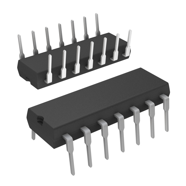
From an integration and footprint perspective, the 14-pin TSSOP package is a crucial enabler for dense PCB layouts, allowing circuit designers to consolidate monitoring or signal conditioning stages into a singular, compact device. This is particularly valuable in wearables, sensor modules, and IoT nodes where board space and weight drive core requirements. Deploying the TS334IPT in such scenarios often results in streamlined BOM counts and simpler board routing, directly contributing to design cycle acceleration and long-term product maintenance ease.
Within level-shifting and window comparator applications, the quad-channel arrangement offers the granularity to monitor multiple thresholds or implement complex detection algorithms without duplicating discrete active components. Practical deployment confirms that integrating all four comparators often yields lower total system leakage and glitch-free state transitions, compared to chaining singles or duals, particularly under fast dynamic input changes.
A core observation is the device’s seamless scalability across power supply architectures; circuits employing dual-rail or single-cell topologies can leverage the same part number, reducing inventory complexity. Furthermore, the highly predictable propagation delay— largely unaffected by supply voltage reduction— simplifies timing margin calculations for time-sensitive digital interface monitoring.
TS334IPT’s feature set not only aligns with foundational comparator use cases but also anticipates evolving requirements in connected and energy-harvesting domains, where long operational lifetimes and reliable edge detection are paramount. This convergence of low power, small footprint, and analog integrity defines TS334IPT as a comparator of choice in the transition towards smarter, more autonomous embedded solutions.
Key features and advantages of TS334IPT STMicroelectronics
TS334IPT from STMicroelectronics exhibits a set of technical characteristics highly aligned with the demands of modern analog front-end design. Its supply voltage range, extending from 1.6 V to 5 V, permits seamless integration into mixed-voltage architectures, supporting both contemporary low-voltage nodes and established 5 V logic families. This feature proves especially advantageous when designing systems that must bridge microscale IoT elements with legacy industrial platforms without resorting to complex level-shifting protocols or additional regulators.
The device’s remarkably low quiescent current draw—20 μA (typical)—enables its use within battery-constrained environments, where prolonging operational lifespans or minimizing self-discharge is critical. Deploying the TS334IPT in sensor interfaces, remote asset monitors, or compact medical instrumentation demonstrates its capacity to balance performance with power prudence. In fabrication, this characteristic often yields the freedom to increase circuit density while remaining within strict total current envelopes.
Its rail-to-rail input structure serves to maximize the exploitation of available signal swing without loss of comparator response near supply extremes. This is a key attribute when input common-mode voltage approaches either supply rail, as frequently observed in single-supply systems. Such an architecture allows placement at critical signal boundaries, ensuring consistent functionality even as input voltages traverse their highest dynamic range. In mixed signal boards, successful implementation mitigates margin loss, especially in sensor readouts or ADC interface preprocessing stages.
An open-drain output architecture introduces significant topological flexibility. Designers benefit from native wire-OR logic capability, straightforward interfacing to various voltage domains, and the choice of external pull-up resistors tailored for speed or power constraints. In level-shifting solutions, particularly where isolation between domains is required via optocouplers or transceivers, this output style simplifies the design pathway and maintains compatibility across a wide spectrum of logic families.
Propagation delay is tightly controlled, with typical values down to 210 ns. Fast response is paramount in zero-crossing detectors, digital event discriminators, and PWM feedback loops, where timing uncertainties directly affect system accuracy or control bandwidth. Field observations confirm that such short delays translate to a marked improvement in signal edge fidelity, ensuring prompt system reaction without introducing overshoot or instability.
ESD robustness, rated up to 2 kV (HBM) and 200 V (MM), signifies resilience within noisy industrial and automotive environments. When deployed on exposed PCBs or in high-transient regions, this degree of protection reduces post-deployment failures related to static charges or inadvertent contact, allowing for cost containment and reliability scaling. For automotive modules subjected to repeated handling and varying grounding quality, high ESD tolerance is fundamental.
The specified temperature range from –40°C to +125°C guarantees reliable performance across climates and mission profiles. This flexibility enables confident integration into outdoor installations, high-variation industrial nodes, and automotive ECUs. From lab prototyping to field deployment, such temperature stability is repeatedly shown to prevent performance drift and unanticipated shutdowns.
When selecting comparators for space-constrained, energy-sensitive analogue or mixed-signal designs, TS334IPT consistently demonstrates operational reliability, integration efficiency, and resilience. Common pitfalls such as input offset drift, unexpected leakage, or timing jitter are minimized by its well-engineered feature set, which supports robust subsystem development even under challenging environmental or operational conditions. Ultimately, the interplay of rail-to-rail input, minimal current consumption, flexible output, and high ESD survivability leads to design paths characterized by lower risk, accelerated development timetables, and maximized functional density.
Absolute maximum ratings and operating conditions of TS334IPT STMicroelectronics
Absolute maximum ratings for the TS334IPT delineate the boundary conditions under which the device can operate without compromising integrity. All external and internal voltage references are measured relative to the device’s main supply rail, which standardizes performance expectations in both single- and split-supply designs. This normalization simplifies integration within larger systems, minimizing variation due to grounding anomalies and reducing node offset errors, which is critical in sensitive analog front-ends.
Thermal resilience is a core attribute, especially given the specified –40°C to +125°C operating temperature range. This wide spectrum ensures the comparator can maintain stable response in applications exposed to frequent thermal cycling—automotive ECUs, outdoor sensor nodes, or industrial controllers. Experience shows that maintaining junction temperatures within this envelope, even during prolonged full-load conditions, leads to predictable propagation delay and offset voltage characteristics over field life.
Electrical and thermal limits are anchored by adherence to established standards such as JESD22-A114F/A115A for ESD and ANSI/ESD STM5.3.1. These protocols subject devices to rigorous human-body model and charged-device model stress testing, certifying resistance to common handling and board-level assembly exposures. In deployment, the device withstands typical PCB-level surges, such as those from cable plug-in events or switching relays, without latent performance degradation—a significant reliability factor in mission-critical or consumer equipment where serviceability is limited.
Application reliability hinges on strict observance of absolute maximum ratings for voltages, currents, and power dissipation. Scenarios such as power sequencing, supply transients, or rapid input switching often create brief excursions near these bounds. Effective designs incorporate RC snubbers or clamp diodes at vulnerable nodes, especially at input or output pins, providing an additional buffer against overshoot or undershoot incidents. Focus on layout symmetry and minimizing parasitics further assists in avoiding localized overstress, which may not register instantaneously as damage but initiates performance drift over time.
An implicit insight: The success of robust system design with the TS334IPT lies not just in respecting the published “do not exceed” parameters, but in embedding margin and fail-safes at both schematic and layout level. Comprehensive pre-deployment testing, simulating the worst-case supply ramp and ESD events, reveals circuit vulnerabilities otherwise masked in typical bench evaluation. Consequently, field longevity becomes a function of both the device’s engineered resilience and the application’s attention to operational nuances, reinforcing the necessity of coordinated protection strategies beyond datasheet consultation.
Detailed electrical characteristics of TS334IPT STMicroelectronics
The TS334IPT from STMicroelectronics presents a compelling profile for signal processing architectures demanding both low power and high accuracy. At its core, the supply current reflects a tightly controlled relationship with applied voltage, anchored by a typical quiescent draw near 20 μA. This characteristic directly impacts battery-powered and energy-critical systems, ensuring minimal overhead and promoting extended operational cycles without sacrificing responsiveness.
Examining the input stage, emphasis on low input bias currents translates to seamless compatibility with high-impedance sources. Sensor applications benefit from this attribute due to diminished signal corruption and increased sensitivity, particularly in environments where leakage and loading must be suppressed. The input offset voltage exhibits thermal stability, minimizing drift across varying operational ranges—an essential consideration when signal fidelity must persist over extended deployments and temperature fluctuations are expected.
Output capabilities are engineered for consistency, with saturation voltages held close to rail yet always predictable across the full supply spectrum. The device supports robust sink currents, which secures reliable state transitions when driving loads or interfacing with downstream logic. Applications leveraging this stability include analog threshold comparators and level shifters, where output certainty directly influences system correctness.
Internally, propagation delay metrics, often cited near 210 ns, reveal subtle modulation under conditions of high overdrive or shifting common-mode voltage. Accurate interpretation of datasheet timing charts offers actionable insight; in fast edge detection and precise pulse discrimination scenarios, recognizing this delay variation is vital to ensure correct event capture and downstream triggering synchronization. Integration into time-critical chains thus demands not only device selection but also tailored circuit layout—grounding paths and minimizing parasitic capacitances further optimize speed.
Temperature dependence, as mapped in manufacturer-provided graphs, completes the behavioral profile. Variations in supply and input/output parameters across the temperature envelope instruct simulation and board-level prototyping, allowing anticipatory mitigation of drift and preventing unforeseen instability under field exposure. The ability to anticipate these shifts adds robustness, especially in industrial or outdoor environments.
An advanced perspective recognizes that effective integration hinges on understanding not merely datasheet figures but also dynamic interactions in the intended application. Device nuances such as weak coupling between input bias and output characteristics under edge temperature cases can be engineered to advantage in redundant or fault-tolerant configurations. The TS334IPT’s characteristic balance between low power draw and high signal integrity positions it as a strategic building block, particularly where precision sensing, reliable threshold detection, and predictable digital interfacing are prioritized within compact form factors.
Package types and mechanical data for TS334IPT STMicroelectronics
Package types and mechanical data for the TS334IPT from STMicroelectronics present essential considerations for integration in modern PCB designs. The TS334IPT arrives in a compact 14-pin TSSOP form factor, a choice that optimizes board real estate and aligns with industry-standard surface-mount assembly workflows. This package balances small footprint requirements with sufficient lead pitch (typically 0.65 mm) to facilitate both automated pick-and-place accuracy and reliable solder joint formation during reflow, mitigating the risk of bridging or cold joints that sometimes complicate denser packaging platforms.
The mechanical specifications, detailed in the supplier’s datasheet, serve as foundational inputs for footprint generation within ECAD tools. PCB designers must leverage these reference dimensions precisely, including recommended pad sizes and standoff profiles, to ensure optimal solder fillet formation and to accommodate board flex or process-induced tolerances. Misalignment between the mechanical footprint and the actual land pattern often leads to unintended yield losses in mass production or latent reliability issues, such as poor joint strength after multiple thermal cycles. In multi-channel or analog subsystems where the TS334 family excels, proper pad design also influences electrical performance by controlling parasitic inductance and capacitance near the device leads.
Further, the TS33x family’s package versatility accommodates diverse application constraints. For higher pin-count requirements or alternative assembly flows, variants such as the SO14 or QFN16 offer differentiated thermal dissipation profiles and reduced package height, expanding deployment options in space- or weight-critical applications. In tightly stacked designs, QFN packages provide superior heat transfer paths to the PCB, supported by the exposed thermal pad, but demand precise stencil design and X-ray inspection protocols to verify solder integrity.
From an environmental standpoint, all package versions adhere to STMicroelectronics’ ECOPACK processes. Materials selection and lead finish comply with major international hazardous substance restrictions, positioning boards populated with the TS334 family for seamless acceptance in regulated markets and automated RoHS documentation workflows. Integrating ECOPACK-compliant components at the schematic stage pre-empts end-of-cycle compliance rework, an often overlooked but significant engineering efficiency gain.
In practice, synchronized mechanical and environmental documentation—backed by up-to-date manufacturing application notes—streamlines pre-fabrication DFM and DFA reviews. Incorporating package data not only at the component selection stage, but as part of a continuous iteration with PCB fabricators and assembly partners, ensures the TS334IPT and its family variants perform predictably across prototyping and scale-up phases. This holistic integration of mechanical, manufacturing, and environmental objectives ultimately underpins robust analog signal chain deployment across consumer, industrial, and instrumentation domains.
Application scenarios and engineering considerations for TS334IPT STMicroelectronics
TS334IPT from STMicroelectronics exemplifies a modern micropower comparator tailored for applications requiring both stringent energy management and robust analog performance within space-constrained systems. The device’s core advantage lies in its ultralow quiescent current, which brings significant value in mobile and battery-dependent environments. For health monitoring wearables and portable instrumentation, the minimized supply current not only extends service intervals but also supports always-on sensing modes without materially degrading battery reserves. This low-power behavior, combined with a broad supply voltage operating range—typically from 1.8V to 5.5V—allows seamless integration with both traditional and emerging microcontroller platforms in distributed or wireless sensor nodes.
In the context of input threshold detection—an essential function in notebooks, tablets, and legacy PDAs—the TS334IPT provides clear, stable transitions even at reduced voltage rails. Designers can exploit the device’s rail-to-rail input topology to maximize signal swing utilization, critical for accurately detecting system states or external events in modern power-managed logic. The open-drain output architecture, when paired with appropriately dimensioned pull-up resistors, enables direct interfacing with diverse logic families and facilitates straightforward level shifting, which is advantageous in designs spanning multiple supply domains or implementing wired-AND functions. Careful attention to output impedance and the choice of pull-up value becomes necessary to balance propagation delay against power dissipated in the passive network—an engineering trade-off often overlooked in initial schematic iterations.
For industrial and automotive deployments, TS334IPT delivers resilience under thermally and electrically demanding conditions. The wide ambient temperature range and suitable automotive qualification unlock use in equipment such as remote sensor modules, process control boards, and underhood diagnostic interfaces. Here, the fast response and robust input stage offer immunity to typical field-level transients and slow-varying analog inputs encountered in harsh mission profiles. Practical application reinforces the importance of validating comparator behavior under noisy supply transients, often by bench-prototyping with real-world loads to reveal interaction nuances between the device, upstream sensing networks, and downstream digital acquisition chains.
From an architectural perspective, the rail-to-rail configuration empowers not just low-voltage operation but also high input common-mode range, supporting input signals nearly at the supply rails—a necessity in precision instrumentation and interfacing with modern DACs and sensors. Selection processes should include detailed compatibility checks for output drive capability, aggregate bias currents, and logic levels with the target processor ecosystem. In multi-domain systems, open-drain outputs offer indispensable flexibility, but demand rigorous attention to layout practices minimizing crosstalk and unintentional leakage paths, particularly when several comparators share signal routing.
Ultimately, TS334IPT’s balanced feature set, including package miniaturization and cost efficiency, encourages its proliferation across a variety of low-voltage, high-reliability analog front ends. Direct field experience underscores the device’s value in projects with severe board-area constraints or prolonged energy autonomy requirements, particularly where comparator input/output behavior must be unambiguously predictable under all operational scenarios. A nuanced appreciation of system-level interactions—extending from schematic capture through to EMC compliance testing—maximizes both the functional benefits and deployment reliability of this analog building block.
Potential equivalent/replacement models for TS334IPT STMicroelectronics
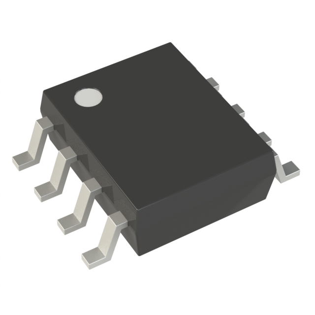
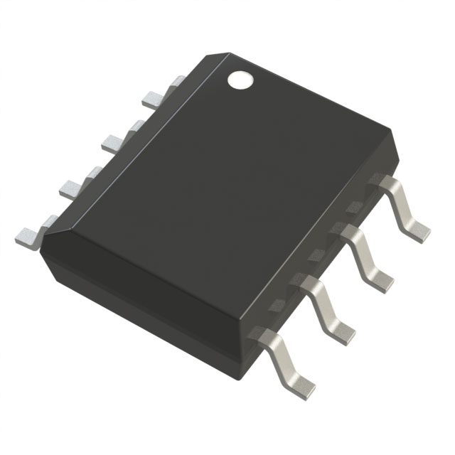
Within the context of comparator selection for signal conditioning and discrete-level detection tasks, the TS334IPT belongs to a broader STMicroelectronics TS33x product family that emphasizes pin-to-pin scalability and consistent electrical characteristics across variants. The TS331, TS332, and TS334 provide single, dual, and quad-channel configurations respectively, supporting streamlined design upgrades or cost optimization by enabling direct substitution based on channel requirements while preserving the fundamental analog performance envelope. Available package formats—such as SOT23-5, SC70-5, DFN6, SO8, MiniSO8, DFN8 (with and without wettable flanks), QFN16 3x3, SO14, and TSSOP14—facilitate layout flexibility across diverse PCB constraints, from high-density consumer applications to robust industrial equipment.
Evaluating potential replacement pathways for the TS334IPT necessitates a two-level analysis. At the base layer, form factor and pinout compatibility drive short-listing to ensure seamless drop-in replacement, especially in compact QFN, SO, or TSSOP outlines where layout rework is cost-prohibitive. The TS33x series distinguishes itself by maintaining identical input structures, propagation delays, and power profiles across its variants, reducing qualification burden for design engineers targeting legacy board architectures. This intrinsic consistency limits the risk of introducing subtle analog artifacts due to offset drift or comparator speed mismatches when increasing or decreasing channel counts.
The next selection stage centers on functional parameters that impact application reliability, such as input common-mode voltage range, output drive capability, and supply voltage tolerance. For applications with strict timing or low-voltage logic interfaces—such as portable medical instrumentation or automotive sensor modules—scrutiny extends to propagation delay dispersion and quiescent current ceilings. While alternative comparators from STMicroelectronics or other vendors (such as Texas Instruments LM339 series or ON Semiconductor LMV393 family) may offer similar core functions, minor differences in hysteresis implementation, output topology (open-drain vs. push-pull), or ESD robustness may influence overall system noise immunity and fault tolerance.
A practical design strategy involves empirically confirming substitute performance under final-use conditions, particularly in scenarios involving fast transient signals or proximity to supply rails. Floating supply fluctuation and ground bounce effects, for instance, may reveal edge cases where theoretically equivalent devices diverge in output stability or recovery behavior. Another consideration is vendor supply chain resilience; alignment to a popular comparator footprint can streamline dual-sourcing, ensuring continuity during component shortages without iterative revision cycles. Leveraging parametric search tools and cross-referencing reference designs from the TS33x datasheets and application notes provides further confidence in functional equivalence, especially when targeting certification in regulated environments.
In summary, the TS334IPT and its TS33x family stand out for their engineering-centric focus on scalability, minimizing integration friction across successive design evolutions. When qualifying direct replacements within or outside the series, structured attention to both mechanical footprint and subtle analog performance nuances enables robust specification adherence and long-term manufacturability. This layered methodology establishes a resilient foundation, even as operational envelopes shift or supply chain dynamics evolve.
Conclusion
TS334IPT from STMicroelectronics integrates a robust set of analog comparison capabilities particularly well suited to environments where precision, efficiency, and resilience are required. Its core architecture leverages micropower consumption, supporting extended battery lifespans and minimizing thermal stress—attributes critical in low-power sensor interfacing and remote-control nodes. The device incorporates rail-to-rail input stages, allowing it to process wide input voltage ranges even near supply rails without sacrificing signal integrity, a key advantage in complex mixed-signal boards and multiplexed analog front ends.
Open-drain outputs facilitate flexible level shifting and direct interface with digital logic, streamlining system integration and allowing designers to tailor pull-up strategies for noise immunity or speed constraints. The comparator’s inherent input protection and electromagnetic compatibility augment longstanding reliability in harsh industrial and automotive domains, where transient voltages and unpredictable ground references challenge conventional analog circuits.
Multiple packaging options, including space-efficient surface-mount formats, support dense PCB layouts often seen in automotive ECUs and high-uptime industrial controllers. The electrical characteristics—such as input offset voltage, response times, and output current capacity—enable precise threshold detection in battery management, fault monitoring circuits, and operational amplifiers for control loops. Experience shows that the TS334IPT’s predictable behavior across temperature and voltage extremes reduces system-level risk, easing compliance with stringent quality and regulatory requirements.
Integrating the TS334IPT streamline analog signal discrimination tasks, providing robust building blocks for ADC pre-conditioning, overcurrent or overvoltage sensing, and window comparator configurations. The device’s design anticipates the shifting landscape toward tighter integration and more distributed intelligence, staying effective even under aggressive EMC profiles and supply variability. Application teams benefit from consistent parametric performance, forging stable long-term platforms with minimized need for analog redesign cycles. TS334IPT demonstrates a convergence of versatility and reliability, providing engineers a foundational comparator solution that scales from compact IoT nodes to mission-critical automotive safety systems.