 >
>


Product overview of TS331ICT STMicroelectronics
The TS331ICT occupies a specialized niche in the spectrum of low-voltage comparators, tailored for ultra-efficient signal comparison tasks within battery-powered and space-constrained applications. Engineered around a micropower architecture, it achieves minimal quiescent current consumption while maintaining consistent precision across a supply range of 1.6 V to 5 V. This characteristic not only reduces energy drain in standby or always-on monitoring scenarios but also lessens thermal impact, a critical consideration in tightly integrated, miniature layouts.
At the circuit level, the rail-to-rail input stage extends the functional input voltage range to the full supply boundaries, enabling accurate signal discrimination even when input signals approach ground or Vcc. Such linearity across the rails proves advantageous in sensor interfaces and threshold detection systems, where voltage swings can be unpredictable yet must be processed reliably. The open-drain output topography further enhances configuration flexibility; it allows seamless interfacing with external pull-up resistors, supports logic-level shifting, and simplifies wired-OR implementations for fault detection or aggregation logic.
From a packaging perspective, the SC70-5 footprint substantially optimizes PCB real estate, facilitating dense layouts demanded by next-generation portable devices. This minimized physical profile inherently supports automated assembly lines and high-volume manufacturing, mitigating cost and reliability risks tied to manual intervention. When integrating the TS331ICT, designers routinely leverage its low input bias current and fast propagation delay to ensure responsive system behavior, particularly in battery management, low-frequency monitoring, or on/off control loops.
The comparator’s role can be expanded through clever circuit topologies: for example, in precision voltage thresholding within energy harvesting modules, the TS331ICT provides deterministic outputs even under rapidly varying supply conditions. In my view, the device’s robust input tolerance and ability to function at near-depleted battery levels position it as a foundational element in power-sensitive analog signal chains. The broader TS33x family, encompassing dual and quad channel variants, streamlines scalable designs when multi-point monitoring or multi-path logic becomes necessary, eliminating the need for piecemeal comparator arrays and simplifying BOM management.
Practical deployment highlights the importance of board-level isolation and careful routing to capitalize on the comparator’s high input impedance. In mixed-signal environments, attention to grounding strategy and bypass capacitor placement directly influences noise immunity and signal fidelity, ultimately determining system reliability. The convergence of power efficiency, package dimension, and electrical adaptability in the TS331ICT reflects a design paradigm increasingly adopted in portable analytics, miniaturized IoT, and medical sensor platforms—where every milliwatt and square millimeter count.
Through continual platform evolution, including compatibility with modern logic voltage domains and stable performance under varied temperatures, the TS331ICT emerges not just as a utilitarian comparator but as an enabling component for future-forward, energy-conscious circuit innovation.
Key features and benefits of TS331ICT STMicroelectronics
The TS331ICT comparator from STMicroelectronics is engineered to address the pressing requirements of modern low-power, precision electronics. Its broad supply voltage range, spanning from 1.6 V to 5 V, directly supports compatibility with advanced low-voltage logic circuitry and battery-centric architectures. In battery-operated sensor interfaces, designers achieve robust operation across fluctuating battery conditions without compromising detection integrity or logic thresholds.
Ultra-low quiescent current, specified at a typical 20 μA, is particularly effective in reducing system-level power budgets. This attribute is essential in portable and always-on devices, such as environmental monitors and wearable medical sensors, where extended deployment periods are required without frequent battery replacement or recharging. The comparator’s negligible power draw enables aggressive sleep and power-down strategies at the system level, ensuring that the analog front end does not become a limiting factor in overall energy efficiency.
The inclusion of rail-to-rail input capability extends the TS331ICT’s versatility in sensing scenarios. Designers benefit from precision across the full supply voltage span, enabling accurate monitoring of signals close to either rail without distortion or loss of sensitivity. Situational use in MCU-based platforms, where MCU supply voltages and sensor outputs vary or drift with supply changes, further illustrates the necessity of such an input range for reliable detection across diverse application landscapes.
Thermal resilience is built into the device, as evidenced by the −40°C to +125°C operational range. This specification substantiates suitability for both automotive and industrial deployments, where ambient temperatures are volatile and rigorous qualification standards exist. Such endurance ensures consistent response and threshold performance, even under continuous thermal cycling or in proximity to heat-generating loads.
A low output saturation voltage, paired with a typical propagation delay of 210 ns, optimizes the TS331ICT for precision timing and high-frequency switching tasks. Practical use cases include overcurrent protection, clock supervision, and configurable reset circuits in embedded systems. The minimized voltage drop at the output translates to reduced static losses and clean interfacing with subsequent digital processing stages, particularly in logic circuits with tight margin constraints. Fast propagation further guarantees timing fidelity, an often-overlooked limitation in comparator selection that can dictate the responsiveness of fault-detection and control circuits.
The open-drain output architecture enhances logic compatibility, enabling straightforward level shifting and multipoint wired-AND operations. This is particularly effective in multi-voltage digital environments or in shared-alert lines, where multiple comparator outputs must safely coexist on a common node. Such flexibility simplifies board layout and system integration, and sidesteps the typical challenges encountered with push-pull outputs in complex mixed-signal designs.
Electrostatic discharge protection—up to 2 kV human body model (HBM) and 200 V machine model (MM)—offers practical insurance against handling and assembly stresses, which remains critical at scale and during field servicing. This robustness factor reduces costly field failures and extends module reliability in harsh environments.
A core insight emerges from the convergence of these features: the TS331ICT can serve as a fundamental analog monitoring element across a spectrum of challenging applications, where supply efficiency, signal integrity, and robust interfacing are not optional but essential system attributes. Selective deployment of this device frequently leads to streamlined design cycles, as its architecture reduces the need for additional signal conditioning or protection components. Consistently, field experience reveals improved long-term stability and ease of certification in safety or mission-critical systems due to its balanced blend of electrical and mechanical durability. This intersection of efficiency and versatility distinguishes the TS331ICT as an enabling product in the contemporary analog design toolkit.
Electrical characteristics and performance of TS331ICT STMicroelectronics
The TS331ICT comparator from STMicroelectronics is engineered for dependable performance across a multi-rail supply environment, offering stable electrical characteristics that simplify selection in demanding systems. Its functionality at supply voltages of 1.8 V, 2.7 V, and 5 V ensures adaptability, with minimal variation in critical parameters such as supply current, propagation delay, and input offset voltage. At the lowest rail of 1.8 V, the device sustains low supply current and achieves short, consistent propagation delays, which is essential for low-power, portable applications where power envelope and reaction time are tightly constrained. The controlled input offset voltage and input bias current, both maintained within nominal ranges, mitigate drift and error accumulation, supporting precision even as substrates scale down or noise floors rise.
Analyzing the propagation delay (both TPHL and TPLH) reveals that timing consistency is preserved across the input common-mode range. This consistency is crucial in time-critical signal processing, such as window comparators or threshold detection circuits in industrial control. High-speed architectures benefit from such timing fidelity, ensuring that output changes track fast-moving input signals without introducing unwanted latency or signal skew, even at reduced voltage levels.
Efficiency in digital logic interfacing is further realized in the TS331ICT’s output stage. The comparator delivers low output saturation voltages, minimizing losses during logic state changes under varying sink currents. As a result, downstream digital logic can reliably interpret comparator outputs with minimal ambiguity, improving noise margins and enhancing system stability. This characteristic is particularly advantageous in multi-channel or multiplexed analog front-ends, where line loading and channel crosstalk can otherwise degrade logic transitions.
Thorough evaluation is supported by STMicroelectronics’ detailed datasheet, including performance curves covering supply current as a function of supply voltage, propagation delay response to differential overdrive, and the variation of output voltage under differing loads. Leveraging these resources, engineers can benchmark system-level behavior before integration, anticipating operational margins in diverse deployment scenarios. In environments subject to thermal fluctuations or stringent EMC requirements—such as automotive sensor interfaces or high-density sensor nodes—the temperature-dependence graphs for input offset and bias current further inform robust thermal management and system calibration strategies.
From practical deployment, it is evident that early-stage validation using these comparator characteristics streamlines board-level debug and accelerates bring-up cycles. An implicit design advantage arises from the comparator’s ability to maintain key parameters across real-world voltage rails and temperature excursions, reducing the need for frequent recalibration or extensive guard-banding during design verification. This enables the TS331ICT to serve as a drop-in solution for mixed-voltage platforms, further supporting rapid prototyping and reliable scaling in volume production. A comparative analysis suggests that the device’s balance of speed, power, and stability provides a strong foundation for designing next-generation analog-to-digital interfaces and precision monitoring modules, with system-level resilience emerging from its core performance profile.
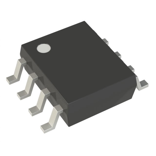
Mechanical and packaging information for TS331ICT STMicroelectronics
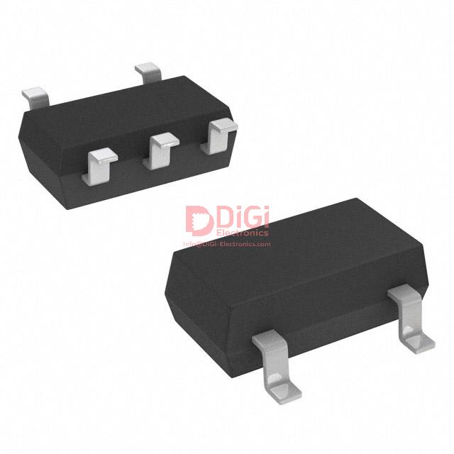
The TS331ICT from STMicroelectronics leverages the SC70-5 (SOT323-5) package, which epitomizes the trend toward ultracompact integration for space-constrained designs. The enclosure measures a minimal 2.0 × 1.25 mm, supporting high component density without compromising mechanical robustness. Such dimensional precision aligns with industry-standard tolerances, streamlining automated pick-and-place operations and optimizing soldering yields in high-throughput SMT environments. Standardized pin-out conventions enable direct insertion into generic, pre-qualified footprints, reducing the risk of misalignment or tombstoning during reflow.
The SC70-5’s low profile and minimized lead pitch address the dual challenge of board space and assembly reliability in advanced applications. In practice, the fine-pitch geometry requires controlled solder paste deposition and well-calibrated reflow profiles; these parameters directly influence solder joint integrity and the long-term reliability of densely populated PCB assemblies. The package’s moisture sensitivity classification (typically level 1 or 2a for STMicroelectronics variants) further minimizes concerns during reflow cycles, lowering exposure risks in automated production and field deployment.
Beyond SC70-5, the TS33x family’s footprint diversity encompasses SOT23-5, DFN6, SO8, MiniSO8, QFN16, SO14, and TSSOP14, targeting a variety of system integration needs. For instance, engineers often select QFN or DFN versions to leverage reduced parasitics and improved thermal performance for high-frequency analog front-ends, while SO and TSSOP solutions remain favorable where legacy compatibility and assembly process robustness are prioritized. Footprint scalability supports migration across platforms and product variants with minimal redesign, preserving signal integrity and thermal management characteristics.
Design decisions for the TS331ICT frequently pivot on the SC70-5 package’s suitability for applications such as wearables, IoT edge nodes, and compact medical devices. In these contexts, real-world deployments underscore the merits of reduced package dimensions when managing strict EMC requirements and mixed-signal routing within sub-assembly enclosures. Empirically, effective layout involves maintaining clear pin-1 marking in silkscreen and referencing IPC-7351-compliant footprints—choices that reinforce assembly error tolerance and accelerate DFM validation. Engineers often capitalize on the package’s symmetry and standardized pin mapping to streamline test fixture design and in-circuit test coverage.
A key insight emerges from the interplay between physical miniaturization and assembly process control. As package scales shrink, the margin for error narrows: precise land pattern definition, stencil design, and reflow profiling become decisive for yield and repeatability. The SC70-5 format, as implemented in TS331ICT, finds its optimal balance here, enabling innovative, dense system-level solutions while upholding manufacturability and operational reliability. This synergy enables accelerated development cycles, pushing the envelope for next-generation embedded electronics.
Typical applications of TS331ICT STMicroelectronics
TS331ICT from STMicroelectronics exemplifies design adaptability, catering to a spectrum of compact and power-sensitive systems. The device operates as an ultra-low power comparator with rail-to-rail input capability, which directly addresses voltage discrimination challenges within portable hardware architectures. Its minimal quiescent current—typically 0.6 µA—ensures negligible impact on overall system power budgets, a pivotal factor in battery-centric designs such as remote sensor nodes or compact medical instrumentation. The device’s extremely small footprint lends itself well to aggressive PCB space constraints, commonly encountered in next-generation mobile handsets and wearables.
Voltage monitoring remains a critical task in mobile phones, tablets, and personal digital assistants, where instantaneous and precise detection of undervoltage or overvoltage conditions must be implemented without sacrificing battery lifetime. Integrating TS331ICT as the core comparison element enables reliable analog baseline detection for system health, often coupled with microcontroller-based supervisory logic. The comparator’s rail-to-rail input facilitates full span voltage measurement, maximizing fidelity in low supply circuits and permitting a broader array of reference voltages, which turns vital when sensing thresholds are set close to supply rails.
Battery-powered applications, particularly in distributed sensor networks or handheld diagnostic meters, demand robust operation over variable thermal and electrical environments. TS331ICT achieves stability through a wide operating temperature range—spanning from −40 °C to +125 °C—and enhanced ESD protection exceeding 4 kV (HBM), reinforcing fault tolerance in scenarios prone to transient disturbances. Such attributes prove valuable during rapid prototyping phases when interfacing with various analog sensors, as the comparator maintains accuracy despite shifting ambient conditions and unpredictable power inputs.
In embedded control systems, particularly in automotive and industrial contexts, reliable output response time and noise immunity are primary concerns. The TS331ICT delivers propagation delay in the low microsecond range, sufficient to handle edge-triggered logic or real-time alert mechanisms, even in mixed-signal environments where high-frequency sources are present. Its output configuration promotes seamless logic-level interfacing, enabling integration with a broad spectrum of microcontrollers, FPGAs, and discrete logic circuits.
Deployment of TS331ICT accelerates development cycles by streamlining analog design workflows, allowing focus on core system features rather than ancillary comparator circuitry. The device’s engineering-centric attributes—compact form, low power profile, wide voltage and temperature tolerances, robust ESD resilience—underscore its role as a fundamental building block in scalable and reliable solutions. Leveraging these features consistently improves system longevity and reduces maintenance intervals, especially in applications subject to extended field operation or tight regulatory requirements. The intrinsic flexibility built into TS331ICT’s design supports innovative system topologies and facilitates rapid adaptation to emerging standards, providing a practical edge in dynamic product landscapes.
Potential equivalent/replacement models for TS331ICT STMicroelectronics
Selection of comparator models as replacements for TS331ICT from STMicroelectronics involves a multi-dimensional assessment of device characteristics and system constraints. The TS33x family provides variants tailored to specific channel requirements. TS332 integrates two comparators within a single package, optimizing circuit density in designs that necessitate dual-channel assessments, frequently observed in signal monitoring or redundancy frameworks. Availability in SO8, MiniSO8, and DFN8 2x2 formats facilitates flexible PCB layout and footprint matching, critical when retrofitting existing designs with minimal disruption.
TS334 extends this paradigm by offering four independent comparators in QFN16, SO14, and TSSOP14 formats. The quad-channel configuration becomes indispensable in applications such as window detection, multi-threshold sensing, and complex control strategies, where simultaneous comparison across several points is required. Thermally-efficient and space-conscious housing further supports integration in compact modules.
Transitioning to these variants mandates careful validation of electrical continuity with the TS331ICT. Parameters such as supply voltage tolerance, rail-to-rail input range, propagation delay, and power consumption should be cross-referenced with system-level specifications to ensure dynamic compatibility. Open-drain output configurations, common to the TS33x family, support wired-AND logic and ease interface with mixed-voltage domains, preserving signal integrity in both legacy and advanced platforms.
Migration beyond the ST TS33x series imposes additional verification layers. Equivalent comparators from alternate vendors should be mapped against reference datasheets for pin assignment, supply rail limits, common-mode rejection, and input offset. Package matching extends beyond mere footprint—thermal profile, lead pitch, and mounting technology influence manufacturability and reliability in high-density deployments.
In practice, the field reliability of comparator sub-systems correlates strongly with input voltage handling and transient immunity. Designs incorporating TS33x derivatives have demonstrated resilience in noisy industrial environments, courtesy of robust input structures and tolerant ESD thresholds. Open-drain outputs facilitate graceful interfacing with pull-up configurations, a frequent engineering decision when output voltage compatibility is paramount.
A nuanced consideration emerges regarding channel density versus system modularity. Higher-channel comparators, while advantageous for saving board space, may introduce crosstalk or impose layout constraints in analog-heavy domains. Modular selection aligned with application topology—single, dual, or quad—can optimize both performance and maintainability. Where long-term supply continuity is critical, alignment with mechanical standards and electrical performance across manufacturers supports lifecycle management and reduces unforeseen integration risks.
Sophisticated comparator selection builds upon a systemic understanding of channel requirements, electrical landscape, and mechanical adaptation. Strategic filtering of alternative models based on these layers results in robust, scalable designs with predictable performance metrics, streamlining both new product development and legacy platform enhancement.
Conclusion
The TS331ICT comparator, engineered by STMicroelectronics, integrates a micropower consumption architecture within an ultra-compact form factor, directly addressing the stringent demands of contemporary electronic systems where both board space and energy efficiency are critical. Its low quiescent current establishes an underlying platform for extending battery lifetimes and minimizing thermal budgets, particularly relevant in densely packed circuit environments such as mobile devices and portable instrumentation. The wide supply voltage range supports seamless interoperability across diverse power domains, ranging from legacy systems to emerging low-voltage standards.
From an input and output perspective, the TS331ICT implements rail-to-rail input capability and push-pull output stages, optimizing common-mode range and logic compatibility. This configuration enhances reliable switching behavior, reducing susceptibility to noise and tolerances in analog front-end conversion. Such characteristics prove valuable in automotive sensor conditioning and low-voltage signal detection, where error margins must be tightly controlled. Component-level EM immunity and mechanical robustness further reinforce operational stability in harsh electrical and environmental scenarios.
Data-rich documentation—spanning parametric curves, timing diagrams, and recommended PCB layouts—enables effective simulation and evaluation, beneficial for rapid iteration cycles and targeted compliance verification. The TS33x series, encompassing dual and quad variants, furnishes a modular design path, facilitating scalable integration for complex architectures without compromising footprint or uniformity. In prototyping and debugging, standard pinouts and well-defined thermal parameters simplify soldering and rework procedures, decreasing development bottlenecks.
When balancing procurement objectives and design constraints, the TS331ICT affords a synthesis of reliability, configurability, and manufacturability that few direct competitors match. Integrated design flexibility, together with consistent electrical performance under parameter drift and aging, positions the device as an optimal comparator solution in applications prioritizing longevity and precise analog-to-digital interfacing. This capability margin, when exploited through meticulous layout and system-level co-design, yields resilient products that consistently meet evolving application benchmarks.