


 >
>


Product Overview: STR1550 High Voltage Fast-Switching NPN Power Transistor
The STR1550 represents a convergence of advanced fabrication techniques and robust electrical characteristics, delivering efficient high-voltage fast-switching capabilities in a compact SOT-23 package. Underlying its 500 V collector-emitter voltage rating is the implementation of diffused collector planar technology, which minimizes parasitic capacitance and optimizes charge carrier mobility within the silicon lattice. This architecture not only supports swift transition times but also maintains low leakage current, a critical parameter in high-voltage environments susceptible to thermal stress and component fatigue. The 0.5 A maximum collector current enables the transistor to interface with moderate load requirements while sustaining circuit integrity and minimizing losses due to overheating or secondary breakdown—a frequent concern in miniaturized layouts.
Signal fidelity is preserved through the STR1550’s tight switching thresholds and minimal propagation delays, key attributes for driving flyback transformers, timing circuits, and snubber networks in industrial control boards. The device excels when incorporated into pulse-width modulation topologies where rapid on/off cycling and minimized saturation voltage directly impact efficiency and heat dissipation. Practitioners report consistent performance in surface-mount assemblies where PCB space is minimized and airflow is limited, citing the transistor’s ability to withstand surge events without deviation in switching speed or breakdown voltage. Integration strategies often involve paralleling multiple STR1550 units to scale up current-handling capacity, leveraging the uniformity of the SOT-23 footprint for repeatable thermal modeling and layout optimization.
Reliability is further enhanced by the STR1550’s controlled gain characteristics, which simplify analog signal shaping in gate drive circuits and voltage regulation stages. Unlike legacy through-hole power BJTs, the STR1550’s planar design facilitates precise parameter matching and contributes to higher screening yields during volume production. This ensures predictable performance—a decisive advantage in automated test equipment and motor driver modules where component drift can abruptly degrade system tolerance. Notably, the robust isolation rating enables direct interfacing with high-voltage rails without intermediate voltage-clamping, expediting circuit layout and reducing the need for external protection devices.
From a design perspective, the STR1550’s adoption raises the envelope for high-density power conversion and signal modulation, encouraging more aggressive miniaturization without sacrificing electrical safety margins. Such versatility extends to consumer appliances—where power sequencing and high-voltage display drive circuits benefit from its tight electrical control—and to industrial sensing equipment requiring reliable on-off control under variable ambient conditions. The STR1550 sets a precedent for surface-mount high-voltage transistor solutions, demonstrating how material science and process engineering can resolve classic reliability and integration challenges, ultimately broadening the scope of fast-switching power electronics in next-generation embedded systems.
Key Features of the STR1550 Series
The STR1550 series introduces an optimized blend of electrical robustness and package-level versatility, specifically targeted to power circuit architectures demanding high reliability and efficiency. Its DC current gain (h_FE) linearity across an extended collector current range—remaining stable up to 50 mA—addresses the persistent challenge of maintaining signal fidelity in low-voltage, high-gain amplification and predictive switching circuits. This mitigates gain compression and ensures uniform transconductance performance under dynamic load conditions, directly contributing to streamlined feedback control and tighter tolerances in analog front-end designs.
Engineered for high-voltage environments, the STR1550 is characterized by a 500 V collector-emitter voltage ceiling, reducing design risks in circuits prone to transient overvoltages or switching spikes—typical in flyback converters, LED drivers, and motor control stages. The device’s 0.5 A maximum collector current and 500 mW power dissipation rating, specified under standard mounting and thermal management benchmarks, enable integration into densely packed PCBs while adhering to strict thermal design constraints. This supports both continuous and pulsed load profiles seen in load sharing networks and multi-phase converters.
The use of planar structure with advanced base island and edge termination technologies not only optimizes carrier injection profiles but also sharpens switching edges, translating into reduced turn-on/off delays and minimized leakage. These construction techniques expand the device’s safe operating area (SOA), allowing aggressive derating in fault-tolerant systems without compromising transient performance—an essential trait for industrial automation, battery protection schemes, and smart grid nodes.
Logistical efficiency is further enhanced by tape-and-reel packaging, precisely aligned with automated surface-mount workflows. Reliable pick-and-place compatibility and reduced handling errors lower assembly cycle times and boost yield across volume manufacturing, reflecting a nuanced understanding of production realities seldom addressed at the discrete component level.
Complementing the NPN STR1550, the STR2550 PNP variant provides symmetric electrical properties for designers seeking complementary pairings in push-pull stages, H-bridge drivers, and bidirectional power switches. This pairing flexibility promotes modularity and streamlines gate driver configurations, especially in applications where cross-conduction immunity and balanced current handling are essential for thermal integrity.
Practical deployment of the STR1550 highlights its aptness for high-voltage interface translation, inverter output buffering, and protective clamping in relay coils. The device maintains thermal and electrical stability during prolonged operation at rated load, even when subjected to inductive kickback or high dv/dt conditions. One subtle yet consequential observation: the device’s planar structure contributes not only to performance but also to predictable parametric dispersion across production lots, aiding in reproducible circuit modeling and reducing the necessity for extensive post-assembly calibration. This embedded reliability represents an implicit competitive advantage, reinforcing its attractiveness in precision analog and power management domains.
Typical Applications of the STR1550 in Modern Electronic Designs
The STR1550, optimized for high-voltage and rapid switching environments, serves as a central element in contemporary electronic architectures where performance and reliability are non-negotiable. Structurally, its SOT-23 package delivers minimal footprint and thermal consistency, favoring integration into automation-friendly, surface-mount designs and promoting scalability for mass production.
At the device physics level, the STR1550 leverages a refined silicon profile that achieves low output capacitance alongside a stable safe-operating area. This enables operation across demanding voltage swings without overstress or latched breakdown, supporting frequent transitions characteristic of intelligent power management. The switching dynamics are tailored to suppress energy losses at transition points, enhancing efficiency in both burst and continuous conduction regimes.
In LED driving circuits, the STR1550 proves indispensable where maintaining constant current under high-voltage inputs is critical for brightness uniformity and prolonging emitter lifespan. Its expedited turn-on and turn-off behaviors simplify the driving topology for wide-range dimming and enable accurate pulse-width modulation without excessive thermal drift. In high-density lighting arrays, the device supports board-level space constraints, allowing more emitters per unit area.
Industrial control applications benefit from the STR1550’s small-signal amplification at elevated voltages, allowing sensor interfaces and actuator drivers to maintain integrity despite electrical noise or transient disturbances. Here, its gain stability across temperature cycles ensures reproducible response characteristics, reducing calibration overhead.
For power supply topologies, the STR1550 functions effectively in startup and auxiliary switching, where tolerance for voltage spikes and fault isolation are paramount. Integration into snubber networks mitigates high-frequency oscillations, curtailing electromagnetic interference and improving overall supply longevity. Auxiliary circuits also exploit the device’s swift recovery qualities to regenerate bias when transitioning from sleep to active states.
Within display and compact lighting modules, the STR1550 forms the backbone of miniature driver stages. Its fast edge rates enable crisp image rendering and color stability, with package dimensions harmonizing with multilayer PCBs and high-density connector layouts.
In practice, optimized pad layouts and careful thermal management during reflow soldering have demonstrated the STR1550’s capacity to maintain operational stability in tightly packed assemblies, even under aggressive power cycling or extended uptimes. Reliable automated pick-and-place handling further underscores its readiness for large-scale deployment.
Distinctive in its design is the balance between controlled switching waveform integrity and sustained voltage endurance. This enables broader application in hybrid analog-digital signal domains, supporting scalability as architectures evolve toward higher functional integration and tighter spatial-engineering requirements. The STR1550’s role as a low-complexity, high-reliability switching element thus endures across a spectrum of use cases, driving innovation in power-efficient and miniaturized electronics.
Absolute Maximum Ratings and Thermal Performance of the STR1550
A comprehensive understanding of the STR1550’s absolute maximum ratings forms the basis for robust circuit design, particularly where reliability and operational headroom are critical. The principal limits, specified at 25°C ambient under standard PCB mounting, include a Collector-Emitter Voltage (V_CEO) of 500 V, a maximum Collector Current (I_C) of 0.5 A, and a Total Power Dissipation (P_tot) of 500 mW when mounted on a 1 cm² PCB area. These parameters are not mere operational suggestions—they define the safe boundaries, beyond which irreversible degradation or catastrophic failure may occur. Reference to the base current value in the datasheet is essential for precise biasing, since improper drive can compromise switching efficiency or induce thermal runaway.
Delving deeper, the thermal performance is closely linked to both package limitations and board-level thermal management. The SOT-23, by nature of its size, presents a nontrivial thermal resistance from junction to ambient. Even with moderate dissipation, temperature rise within the die can quickly erode allowable margin, especially in environments with limited airflow or increased ambient temperature. This underscores the necessity of maximizing copper area beneath the device and exploiting multilayer PCB structures to spread and evacuate heat. Empirical results consistently show that doubling PCB copper area results in marked reductions in junction temperature, extending device mean time to failure and expanding application versatility. However, diminishing returns set in; careful thermographic analysis often reveals an optimal balance between board space allocation and thermal performance uptick.
Integrating the STR1550 into high-voltage switching topologies, engineers must account for dynamic stresses like collector voltage spikes and repetitive switching losses. Margins against maximum ratings should not only anticipate worst-case input surges but also reflect real-world variances, such as supply instabilities and component tolerances. It’s prudent to dimension boundaries at roughly 80% of listed maximums for sustained reliability in production-grade systems. For example, in high-density power conversion modules, a 500 mW dissipation cap can be the limiting factor; aggressive derating, alongside synchronized drive schemes and optimized snubbing, can mitigate detrimental hotspots and switching transients.
A refined design approach leverages both simulation and thermal imaging during prototyping, facilitating rapid identification of layout bottlenecks and thermal gradients. Iterative rework of the copper pour, via placement, and even silkscreen adjustments can yield significant real-world improvements distinct from theoretical calculation alone. As complexity and power density escalate, these nuanced thermal insights form the backbone of successful STR1550 design-in, serving as the difference between an application that delivers nominal functionality and one that meets rigorous lifetime performance goals.
In summary, strict adherence to absolute maximum ratings, paired with an integrated thermal strategy, enables the STR1550 to perform reliably across diverse use cases—from compact LED drivers to precision instrumentation. Balancing electrical and thermal constraints is not a procedural afterthought but a deliberate and iterative process that ensures both compliance and competitive advantage at the application level.
Detailed Electrical Characteristics of the STR1550
The STR1550 transistor's electrical characteristics are characterized by precise parameterization, enabling highly accurate modeling and circuit optimization. The data, specified at a standard 25°C, provide engineering teams with robust references for both simulation fidelity and real-world predictability. The DC current gain (h_FE) exhibits remarkable linearity across a drive current up to 50 mA, with empirically verified performance at collector-emitter voltages of 5 V and 10 V. This stability in h_FE across typical operating points forms a basis for selecting the STR1550 where gain uniformity directly impacts signal integrity and amplification efficiency.
Examining collector-emitter saturation voltage (V_CE(sat)), the STR1550 offers critical guidance for applications prioritizing minimal power dissipation. The specification covers both low and high h_FE conditions, enabling accurate loss estimation for high-efficiency switching topologies. Design iterations often leverage these saturation values to adjust switching thresholds for reduced thermal stress and improved lifecycle reliability in real-world thermal environments.
Base-emitter saturation and on voltages receive equal scrutiny, as these parameters dictate required drive voltages and influence both switching speed and bias stability. The STR1550’s documentation profiles these voltages for target operation points, ensuring that the device can be reliably incorporated into tightly controlled drive circuits where predictability in dynamic response is crucial. Experience indicates that matching base drive levels to these profiles simplifies gate circuitry and improves tolerance to process variations.
Graphical data embedded in the technical literature amplify the practical value of the STR1550’s specifications. These visualization tools facilitate rapid cross-verification of measured device performance against manufacturer claims, streamlining design validation in both prototyping and production test environments. In various switching and linear application contexts, iterative tuning based on this graphical data has yielded measurable improvements in transition speed, voltage stability, and noise performance.
It is advantageous to perceive the STR1550 not just as a set of static specifications but as a dynamic element within complex architectures. Leveraging the interplay between linearity in h_FE, minimal V_CE(sat), and tailored base-emitter profiles—supported by application-centric graphical analysis—enhances system robustness and simplifies fault isolation. Deploying the device in designs ranging from efficient signal switching modules to precision linear amplifiers is therefore grounded in these layered electrical insights, resulting in circuits that achieve targeted performance with reduced margins for error.
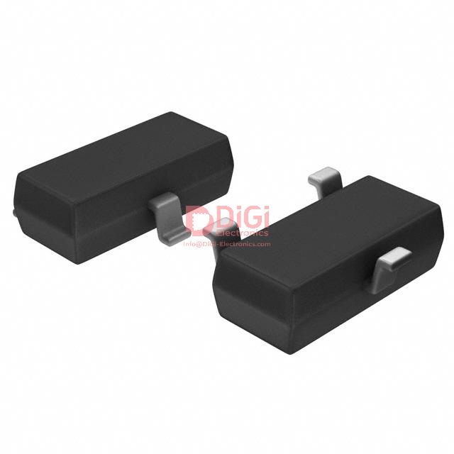
Package and Mounting Details for the STR1550 SOT-23
The STR1550 utilizes the SOT-23 package, a compact, industry-standard format that enables efficient component density on modern PCBs. This package geometry minimizes footprint without sacrificing electrical performance, making it highly suitable for densely populated designs where every square millimeter counts. The SOT-23 outline provides precise dimensions that, when paired with the manufacturer’s recommended PCB pad layout, optimize solder wettability and ensure robust solder joints critical for long-term device reliability in surface-mount technology (SMT) applications.
From a process integration perspective, the mechanical characteristics of the SOT-23—including lead coplanarity, sidewall dimensions, and standoff height—directly influence placement accuracy during automated pick-and-place operations. Robust assembly demands careful adherence to the outlined pad geometry, as deviations can compromise joint quality or induce process defects such as tombstoning. Utilization of solder paste volumes matched to the package specifications supports consistent reflow profiles, reducing thermal and mechanical stresses that may otherwise propagate during production or field operation.
STMicroelectronics further aligns the STR1550 with global compliance mandates by offering ECOPACK-certified variants, directly supporting green manufacturing frameworks and helping to streamline qualification for environmentally regulated markets. The incorporation of standardized tape-and-reel packaging is not merely a logistical convenience; it acts as a critical enabler for high-speed SMT lines, ensuring consistent orientation, minimizing mispicks, and promoting uninterrupted component supply during mass assembly runs.
In practical deployment, leveraging the high pin-to-pin uniformity and dimensional stability of the SOT-23 package translates to fewer post-placement adjustments and consistent yield across production batches. Experience shows that careful review of both land pattern and solder mask design—aided by manufacturer-recommended design libraries—mitigates risks of solder bridging or insufficient joint coverage, particularly relevant as board designs migrate to finer pitches and higher layer counts.
A forward-looking perspective sees the SOT-23 mounted STR1550 as a scalable solution for next-generation electronics demanding not just miniaturization, but also repeatability in manufacturability and environmental stewardship. Thoughtful attention to mechanical, thermal, and material properties at both design and assembly stages empowers engineering teams to maximize device reliability, optimize production throughput, and ensure long-term application success in a highly competitive output environment.
Potential Equivalent/Replacement Models for the STR1550 Series
Identifying suitable replacements for the STR1550 series necessitates careful analysis of multiple device parameters beyond simple pin-to-pin compatibility. The process begins with a comprehensive examination of the target application’s electrical and mechanical constraints. While the STR2550 provides a direct PNP complement to the STR1550’s NPN structure and facilitates the construction of high-voltage push-pull or totem-pole circuits, further consideration should be given to cross-brand alternatives potentially offering process or reliability enhancements.
At the fundamental level, ensuring that candidate replacement devices strictly match the STR1550’s footprint and lead arrangement minimizes layout disruption and assembly risk. Close attention to maximum collector-emitter voltage (V_CEO), collector current (I_C), and power dissipation is critical. Equivalent or slightly improved device thresholds, such as maintaining at least 500 V V_CEO and 0.5 A I_C, safeguard against overvoltage or thermal events during transients. Additionally, subtle package variations—like differences in mold compound or lead frame design—can affect thermal impedance, so measuring junction temperature under realistic loading is advisable during validation.
Parametric alignment alone, however, does not guarantee seamless integration. Secondary parameters—such as gain (h_FE) distribution across temperature, switching speed, and safe-operating-area (SOA) margins—have a significant impact on overall circuit stability and efficiency. Field experience indicates that some devices, while nominally equivalent, may exhibit wider h_FE spread or increased output capacitance, leading to drift in current sharing or slower edge rates. Bench testing under the actual load profile, incorporating transient and repetitive stress, helps expose such mismatches early, reducing late-stage system anomalies.
When evaluating sources from alternative manufacturers, it is prudent to compare process notes and qualification data. Differences in silicon design, passivation, or encapsulation technology may result in varying immunity to high-voltage stress, humidity, or microphonic effects. Engagement with component vendors can yield insights into long-term reliability under specific switching regimes or environmental conditions.
A scalable approach to replacement selection incorporates thermal derating tailored to operational duty cycles, as real-world power transistors rarely function at data sheet maximums. For critical applications, such as industrial drives or line-powered converters, introducing a derating factor—typically 60-80% of V_CEO and I_C—compensates for voltage overshoot and ambient thermal buildup. This margin, verified through staged temperature rise and SOA analysis, underpins robust field performance and minimizes unplanned maintenance.
Ultimately, optimal STR1550 substitution balances rigorous specification matching with practical assessment across the full lifecycle of the target application. Integrating targeted parameter validation, manufacturer dialogue, and in-circuit prototyping leads to well-informed decisions, sustaining circuit performance and reliability even amid supply volatility or process discontinuations.
Conclusion
The STR1550 high voltage fast-switching NPN power transistor from STMicroelectronics is engineered to address key constraints in compact, high-reliability power management circuits. At the core, the device is fabricated using advanced planar technology, enabling a collector-emitter voltage rating that exceeds 400 V while maintaining low collector-emitter saturation voltage even at high collector currents. This foundation supports transient and switching robustness, critical for topologies operating at elevated switching frequencies such as flyback converters and synchronous rectifiers. The SOT-23 package encapsulation is particularly relevant for applications where board area is at a premium, supporting high component density without compromising thermal performance. Careful copper layout under the device footprint optimizes heat dissipation, preventing junction temperature excursions during prolonged switch-on cycles.
Switching speed is another key vector. With sub-100 ns rise and fall times, the STR1550 minimizes power losses during transitions, enhancing system efficiency—a key metric for LED drivers and switch-mode power supplies targeting stringent energy standards. The device exhibits strong current gain linearity across a broad range of collector currents, allowing designers to avoid gain margin over-specification, thereby shrinking the bill of materials and simplifying circuit tuning. This linearity also ensures repeatable circuit response, which is invaluable when scaling to volume production or undergoing regulatory EMI compliance tests.
The inclusion of an environmentally friendly, halogen-free package aligns with global directives on hazardous substances, easing compliance during product certification and facilitating streamlined supply chain approvals. Practical deployment demonstrates the STR1550’s resilience under adverse line and load conditions, with devices maintaining spec compliance even when subject to repetitive avalanche events through proper snubber optimization. This translates to measurable gains in long-term mean time between failure (MTBF) rates in infrastructure and industrial controls.
Additionally, the STR2550 PNP complement expands the topological possibilities. Designers can architect full H-bridges, push-pull stages, or complementary output buffers without incurring excessive sourcing lead time or footprint discrepancies. This symmetry in device options streamlines inventory management and design re-use for platform-based approaches.
Notably, selection of the STR1550 unlocks design headroom in emerging power architectures seeking aggressive downsizing without yield or reliability penalties. The direct integration of robust electrical ratings and compact packaging enables the consolidation of legacy discrete solutions, reducing assembly steps and increasing board-level reliability. This positions the STR1550 as an enabling device for next-generation, miniaturized power subsystems where high voltage endurance, switching speed, and manufacturability converge as competitive differentiators.


