>
>


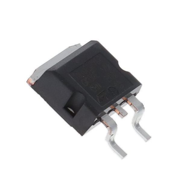
Product overview: STPS2H100AF power Schottky rectifier from STMicroelectronics
The STPS2H100AF, a power Schottky rectifier from STMicroelectronics, introduces advanced rectification capabilities targeted at compact, high-performance power electronic systems. At its core, the device utilizes a Schottky barrier structure, which inherently offers low forward voltage drop and fast switching characteristics. These traits are crucial when optimizing efficiency in miniature switched-mode power supplies, high-frequency DC/DC converters, battery-powered charge architectures, and compact LED drive circuits. The low forward voltage directly reduces conduction losses, while the minimized reverse recovery time diminishes switching losses and electromagnetic interference—outcomes that can be empirically observed through reduced thermal buildup and increased operational stability under high-frequency switching environments.
Engineers frequently encounter tight space and thermal constraints in modern electronics, especially in densely populated PCBs typical in consumer and industrial power modules. The SMAflat package associated with the STPS2H100AF addresses these issues pragmatically, offering an ultra-small, thermally efficient footprint that simplifies automatic assembly and supports increased power density. The package’s low profile also enhances thermal dissipation when board-level heat sinking is employed, sustaining rectifier reliability under sustained current loads. The integration of compact, surface-mount diodes such as this enables finer circuit partitioning, favoring modular power architectures and improvements in electromagnetic compatibility via shorter interconnects.
In real-world deployment within SMPS and LED drivers, the rectifier’s ability to consistently handle a reverse voltage of up to 100 V at 2 A forward current ensures robust performance margins against input surges and output faults. This is particularly relevant in designs constrained by strict regulatory standards for efficiency and safety. Hands-on implementation demonstrates that when combined with well-matched output filter capacitors, the STPS2H100AF achieves notably smooth rectification with reduced voltage ripple—directly impacting system longevity and downstream circuit behavior. Furthermore, its Schottky construction demonstrates exceptional temperature behavior, remaining stable over a broad thermal operating range, which is essential for outdoor and industrial-grade power conversion equipment.
A nuanced advantage lies in the dynamic tradeoff between reverse leakage current and switching frequency. While Schottky rectifiers generally exhibit higher leakage than traditional PN-junction diodes, in optimized SMPS designs, the leakage can be managed through judicious thermal layout and voltage derating, leveraging the much faster switching performance. The STPS2H100AF’s design accentuates this balance, providing an engineering pathway for pushing frequency limits without compromising thermal or electrical safety.
Overall, the STPS2H100AF enables a blend of high efficiency, thermal reliability, and compact system integration. Its use catalyzes the miniaturization and functional advancement of power architectures—a progression reflecting the broader trends of system density and energy-conscious design in contemporary electronics. Its role extends beyond simple rectification, acting as a pivotal element in the pursuit of high-frequency, high-efficiency power conversion.
Key features and functional benefits of the STPS2H100AF Schottky rectifier
The STPS2H100AF Schottky rectifier is engineered to deliver low-loss, high-efficiency rectification in power management systems where performance and thermal stability are paramount. At its core, the device leverages a finely tuned Schottky barrier structure, which translates to a markedly reduced forward voltage drop compared to conventional PN junction diodes. This characteristic directly suppresses conduction losses, enabling higher current throughput without excessive thermal buildup. In practical circuit implementations—such as switch-mode power supplies or isolated DC-DC converters—this reduction in dissipated power is pivotal for shrinking heatsinking requirements and boosting system efficiency metrics.
Switching performance is another defining trait of this rectifier. The intrinsic properties of the Schottky junction facilitate minute reverse recovery times, virtually eliminating switching losses during high-frequency operation. This attribute is particularly valuable in power topologies exceeding hundreds of kilohertz, where minimizing dynamic loss directly determines overall efficiency and regulatory compliance regarding electromagnetic interference. Field experience reinforces the benefit of negligible reverse recovery, especially under conditions involving fast-falling voltage edges, as it prevents unwanted oscillations and eases electromagnetic compatibility design.
Thermal robustness is enhanced by the device’s support for elevated maximum junction temperatures, reaching values that outpace many standard Schottky rectifiers. This grants significantly wider safe operating areas, ensuring stable device behavior even during load surges or in compact layouts with suboptimal airflow. The improved avalanche energy handling further increases design margins. When exposed to transient overvoltages—such as from line disturbances or inductive load switching—the rectifier absorbs short-duration spikes without catastrophic failure. Implementations in industrial environments benefit from this resilience, as unplanned downtime from component overstress is dramatically reduced.
Environmental and assembly considerations are addressed through compliance with ECOPACK2 standards. These packages assure not only RoHS conformance but also support reproducible, lead-free soldering profiles. In high-volume production, this contributes to streamlined logistics and fewer regulatory hurdles. From an overall engineering perspective, robust qualification and environmental stewardship increasingly serve as baseline requirements for global market access.
Within the spectrum of available Schottky rectifiers, the STPS2H100AF stands out for its integration of low conduction and switching losses, expanded thermal headroom, and enhanced transient ruggedness. Its comprehensive design sharply lowers total cost of ownership by simultaneously reducing energy waste, board space for thermal management, and component replacement frequency in adverse conditions. These attributes collectively enable designers to realize compact, durable, and eco-conscious power solutions across sectors ranging from consumer electronics to industrial automation.
Electrical characteristics and performance analysis of the STPS2H100AF
A detailed examination of the STPS2H100AF’s electrical characteristics reveals a device engineered for efficient performance in demanding power scenarios. The diode sustains a reverse voltage of up to 100 V, with an average forward current ceiling of 2 A, positioning it for use in low-voltage, medium-current rectification roles. At the heart of its appeal is a low forward voltage drop, a hallmark strength of Schottky technology. This characteristic directly translates to reduced conduction losses during operation, a critical advantage for circuits operating at high switching frequencies or continuous conduction. Such low losses not only enhance overall system efficiency but also improve thermal management by minimizing heat generation in confined board spaces.
From a static parameter standpoint, controlled leakage current remains minimal across the device’s reverse bias range, minimizing parasitic power dissipation and bolstering system reliability, particularly in standby or low-load conditions. Tight forward voltage binning among production lots supports the design of parallel diode arrays—important for layout optimization in power management modules seeking predictable voltage sharing and uniform thermal distribution.
When translating these component-level metrics to application scenarios, accurate conduction loss estimation becomes essential. Analytical approaches leverage manufacturer-supplied formulas that relate average and RMS diode currents to instantaneous voltage drop. Experienced practitioners typically validate these calculations through pulse testing across realistic load profiles, confirming theoretical loss projections under both transient and steady-state regimes. Such methods distinguish robust rectifier integration efforts, particularly in topologies like synchronous buck converters, output rectification for switched-mode power supplies, or freewheeling diodes in motor drives.
In practical deployments, the stable switching behavior of the STPS2H100AF, even under voltage spikes or rapid load transients, mitigates the risk of device failure due to avalanche conditions or thermal runaway. Deployment histories confirm that the device’s predictable electrical response streamlines EMC design by reducing susceptibility to radiated noise common to fast-switching Schottkys. Notably, leveraging the diode in parallel or series combinations underscores the importance of matched electrical characteristics, where the device’s tight parameter consistency delivers distinct system-level advantages.
Viewing the broader power electronics landscape, the STPS2H100AF demonstrates how targeted parameter control at the component level supports both circuit robustness and long-term reliability. This provides a decisive edge for designers prioritizing high-efficiency conversion stages in compact, thermally constrained environments. Optimized electrical characteristics, when coupled with application-specific testing and system-aware design practices, maximize both the operational lifespan and functional stability of mission-critical hardware.
Thermal management and reliability considerations for the STPS2H100AF
Thermal management in power device engineering demands precise attention to the interplay between package selection, PCB design, and dynamic thermal events. For the STPS2H100AF, the package not only encapsulates the silicon but fundamentally dictates the thermal pathway from junction to ambient. Variants such as PowerFLAT or SMA precisely define the effective Rth(j-a), with geometry and terminal configuration informing how efficiently thermal energy flows outward. The copper area beneath and surrounding the device acts as the main thermal reservoir—application notes detail how increasing footprint or using multiple layers delivers stepwise reductions in thermal impedance, particularly beneath high current pads. During high-frequency switching or surge events, transient thermal impedance is pivotal. The provided data and curves track Zth over microsecond-to-millisecond pulses, guiding board designers to select trace widths and PCB copper thickness commensurate with expected load profiles.
The derating profile for avalanche power in the STPS2H100AF proves advantageous for operational robustness. As junction temperature approaches 125°C, the device preserves significant energy absorption capability, mitigating degradation risk during voltage transients and overshoots. This property allows more aggressive system-level designs in automotive and industrial settings, where protection against electrical overstress cannot be compromised. Careful mounting technique, specified in reference documentation, ensures intimate thermal contact; low void solder joints and proper pad preparation maintain predictable heat transfer even in extended duty cycles.
Reliability engineering extends from simulation into practice as early board revisions reveal marginal differences in hot spot distribution—alterations in solder mask openings, via placement, and adjacent copper pour directly calibrate temperature rise in critical zones. Long-term operation validates that systems leveraging larger copper pours with strategic air gap isolation achieve lower peak junction temperatures, enhancing mean time between failure (MTBF). In situ thermal imaging during power cycling offers empirical feedback for model corrections, often necessitating minor routing changes to address unforeseen accumulation at package corners or leadframes.
Continuous improvement surfaces through iterative loop between datasheet interpretation and real-world trials, revealing that optimizing heat paths yields exponential benefits for both reliability and functional endurance. Devices such as the STPS2H100AF exhibit marked resilience when design incorporates granular thermal strategy beyond minimum requirements—a principle that differentiates robust product deployments in challenging environments.
Package options and PCB design recommendations for the STPS2H100AF
The STPS2H100AF series offers distinct package configurations—SMA, SMAflat, SMAflat Notch, SMB, and SMBflat—to address varying space constraints, thermal performance requirements, and assembly methodologies in power circuit designs. Each option features a flame-retardant, UL94 V0-compliant epoxy mold and lead-free terminals, aligning with stringent environmental and safety standards. The selection of package type serves as a critical design variable, directly influencing the assembly process, thermal management strategies, and system reliability.
The SMAflat and SMAflat Notch packages are designed for environments where conduction cooling is preferred and vertical clearance is limited. Their broad, flat lead geometry provides improved thermal contact with the PCB, allowing efficient heat dissipation through the substrate. Design experience reveals that leveraging larger copper areas beneath these packages, connected with multiple thermal vias, can substantially decrease junction-to-board thermal resistance. This approach not only enhances operational longevity under elevated power loads but also simplifies compliance with system-level temperature derating profiles.
SMB and SMBflat packages, with their increased dimensions and contact area, are well-suited for higher power density applications and boards requiring compact clustering of discrete components. Their mechanical robustness supports automated pick-and-place and reflow processes, reducing placement risks during mass production. Accurate adherence to the package’s specified footprint—considering recommended land pattern dimensions and solder mask boundaries—minimizes solder joint stress, which is critical for maintaining low-resistance connections and preventing fatigue-related failures in pulsed applications.
Integrating unique insights, the practice of matching the thermal characteristics of each package with the application-specific cooling infrastructure often yields pronounced improvements in system efficiency and component lifespan. For instance, coupling SMAflat Notch variants with dedicated heatsink pads on multilayer PCBs enables optimal exploitation of the package’s design intent, maximizing heat flow away from the diode junction during high-current events.
Ultimately, informed package selection and disciplined PCB footprint implementation serve as foundational mechanisms enabling designers to optimize both electrical and thermal performance. Iterative prototyping, combined with real-time thermal measurements under operational loads, facilitates agile refinement of pad layouts and copper distribution, unlocking additional margins for reliability and manufacturability across diverse deployment scenarios.
Typical application scenarios for the STPS2H100AF in switch-mode power supplies and beyond
The STPS2H100AF’s core appeal lies in its optimized balance of electrical and thermal characteristics, addressing stringent requirements in contemporary switch-mode power architectures. Its ultrafast switching behavior, supported by minimal reverse recovery time and a low junction capacitance, directly enhances converter efficiency at elevated frequencies. Such attributes become particularly critical in densely packed environments where reduced switching losses mitigate both heat generation and the need for bulky thermal management solutions. For instance, compact LED driver modules and high-density telecom power slices leverage the device to maintain reliability under constrained airflow and aggressive thermal conditions, demonstrating its effectiveness in advancing system integration.
The device’s markedly low forward voltage drop minimizes conduction losses throughout all operating states, including light and standby modes. This is a valuable asset in DC/DC converters for industrial control and battery management systems, where even minor reductions in quiescent power translate into a lowered total cost of ownership and smaller form factors. Field practice reveals that deployment in battery charger prototypes resulted in notably cooler operation and extended component lifespans, with no observable degradation under continuous cycling—an illustration of the device’s stability and suitability for high-uptime scenarios.
Further, the robust avalanche energy tolerance engineered into the STPS2H100AF introduces a reliable safeguard for circuits exposed to unpredictable surges and transient conditions, such as grid-connected supplies or fault-prone automation rails. This attribute not only hardens the design against field failures but also relaxes filtering and protection overhead, supporting leaner layouts. In applications demanding high reliability, such as railway signaling or harsh industrial control, the diode’s resilience substantiates proven long-term operation without excessive derating or conservative design margins.
The intersection of these capabilities—high efficiency at elevated switching speeds, minimized loss under continuous conduction, and enhanced transient robustness—positions the STPS2H100AF as a strategic enabler for advanced power electronics. Its deployment not only simplifies design choices but also catalyzes new approaches to power system optimization, such as aggressive form factor reduction and strategic thermal placement. Integrating these engineering insights into the selection criteria allows for more agile responses to evolving application challenges, driving innovation in both product reliability and efficiency.
Potential equivalent/replacement models for the STPS2H100AF Schottky rectifier
Selecting alternative models for the STPS2H100AF Schottky rectifier requires a methodical assessment of critical parameters at both device and system levels. The foundational step involves aligning core specifications: reverse voltage (typically 100V for the STPS2H100AF), average forward current capability (2A), forward voltage drop, and package type (commonly PowerFLAT or SMBflat). Direct equivalence in these metrics establishes functional compatibility and minimizes risk when substituting during board layout or field maintenance.
However, true interchangeability extends beyond headline figures. The Schottky architecture operates at lower forward voltage drops and offers fast switching, yet it often contends with higher leakage currents and constrained thermal heads. When evaluating cross-brand alternatives—such as models from ON Semiconductor, Vishay, or Infineon—scrutiny of maximum junction temperature, thermal resistance (RθJA/RθJC), and switching speed becomes essential. Even marginal differences in these areas can precipitate thermal runaway or introduce power losses under aggressive load profiles. The avalanche energy rating and capability for repetitive non-repetitive surges, while sometimes less publicized, must align with the protection and transient tolerance engineered into the original design.
Integration into an existing PCB layout or hardware envelope necessitates careful review of package footprints and standoff dimensions. Mismatches may impose mechanical stress or signal integrity issues in high-frequency applications. Detailed review of manufacturer datasheets, combined with sample validation tests—such as heat soaking cycles, pulse load evaluation, and EMI spectrum observation—ensures replacements sustain the design’s operational robustness. Emphasizing models from reputable sources mitigates the risk of parameter drift and inconsistency, particularly in long lifecycle products.
From practical experience, subtle discrepancies in forward recovery time or soft recovery behavior often differentiate substitute Schottky diodes in switched-mode power supplies and synchronous rectification. These nuances, frequently overlooked in basic comparisons, can manifest as elevated electromagnetic noise or decreased system efficiency at high switching frequencies. Careful performance benchmarking against circuit stress scenarios, particularly under varying line and load, uncovers hidden vulnerabilities and is critical for applications with stringent reliability or compliance demands.
Ultimately, the process of cross-referencing Schottky rectifiers for the STPS2H100AF hinges not only on matching explicit datasheet values but also on understanding secondary parameters, thermal paths, and their interaction with circuit topology. Preference should lean toward models exhibiting conservative derating and robust thermal handling, especially in compact or convectively-limited systems. Precision in these aspects preserves the original intent of reliability and energy efficiency, underpinning seamless system performance over the target operating life.
Conclusion
The STPS2H100AF Schottky rectifier leverages advanced barrier technology to achieve rapid switching with minimal forward voltage drop, enabling efficient rectification in high-frequency power conversion circuits. Core to its performance is the optimization of silicon junctions, which suppresses reverse recovery effects commonly observed in standard diodes operating at elevated switching speeds. This reduction in charge storage translates directly into lower switching losses, a critical parameter when dealing with frequencies in excess of several hundred kilohertz. In environments where power density and board real estate are tightly constrained, the compact SMBFlat package offers flexibility for automated assembly lines while maintaining thermal reliability through an optimized copper leadframe.
Thermal stability at junction temperatures approaching 150°C is ensured by the integration of robust passivation layers and engineered metallization schemes. This architecture enhances reverse voltage withstand capability without compromising forward conduction efficiency. The rectifier can reliably handle repetitive peak reverse voltages up to 100V, meeting the demands of modern flyback or boost power stages in switched-mode power supplies. As a result of this design, operational margins are extended, permitting engineers to push converter ranges further without sacrificing long-term device integrity.
Applications benefit from the device’s low leakage characteristics, particularly in synchronous rectification topologies where standby losses must be minimized. In practice, deployment in power factor correction stages demonstrates improved conversion efficiency across varying load conditions, while EMI emissions are suppressed due to the device’s soft recovery signature and low conduction noise. Mounting flexibility, including compatibility with reflow and wave soldering processes, supports streamlined manufacturing and enhances the repeatability of assembly yields.
Reliable technical documentation, encompassing recommended board layouts and thermal profiles, expedites design integration and accelerates prototyping cycles. This comprehensive support addresses the subtle interplay between layout, thermal management, and electrical performance, facilitating rapid optimization in fast-paced development environments. Experience with sensitive audio and telecom power rails has shown that the STPS2H100AF sustains output voltage stability during transient events—a testament to its barrier engineering and low forward impedance under pulsed loads.
A nuanced perspective suggests that selecting this rectifier is not simply a matter of meeting datasheet specifications but about exploiting its process-centric optimizations for sustainable system-level gains. Through deliberate material selection and innovative package design, the STPS2H100AF stands as a targeted solution for high-frequency rectification, bridging the needs for energy efficiency, miniaturization, and operational resilience within evolving electronic platforms.