 >
>


Product overview of STM32L412RBI6 STMicroelectronics
The STM32L412RBI6 occupies a critical position in the ultra-low-power domain, combining an energy-conscious architecture with substantial processing capabilities. Centered on the ARM Cortex-M4 core equipped with an integrated floating-point unit, the device delivers deterministic real-time performance. Operating at up to 80 MHz and providing up to 100 DMIPS, it supports demanding signal processing tasks while maintaining power budgets suitable for long-term battery operation.
Memory resources are meticulously allocated, with 128 KB of flash and 40 KB of SRAM accommodating secure firmware storage and responsive data buffering. The compact 64-UFBGA package, measuring just 5 mm x 5 mm, facilitates design integration within spatially constrained layouts, a vital requirement for emerging IoT, wearable, and medical platforms. The form factor ensures not just miniaturization but also effective heat dissipation, even when deployed under continuous load or in thermally stressed environments.
From an electrical perspective, the device tolerates a 1.71V to 3.6V operating range, supporting direct connection to conventional battery chemistries and system rails. Its validated ambient temperature range—up to either +85°C or +125°C depending on the variant—enables deployment within high-reliability fields, including industrial and automotive subsystems exposed to severe thermal cycles.
Peripheral diversity enhances the controller's adaptability. The device features advanced analog functions, including fast ADCs, DACs, and comparators with low offset, critical for precision sensor interfacing and closed-loop control. Serial and parallel connectivity is realized through standardized interfaces—SPI, I2C, UART, and advanced timers—supporting protocol stacking, sensor fusion, and motor control with deterministic event capture. Direct memory access (DMA) controllers further optimize throughput and minimize CPU intervention during high-bandwidth transfers, reducing interrupt overhead and suppressing energy spikes.
A foundational aspect is the STM32L4 family's deep low-power modes, including Stop, Standby, and Shutdown, as well as autonomous peripheral operation with the core asleep. These features support multi-year battery life without compromising wake-up speed or peripheral readiness, central to cost-sensitive, always-on deployments. Notably, the dynamic and static current consumption benchmarks achieved in practical instrumented tests routinely meet or surpass competitive MCUs, benefiting edge inferencing and data logging scenarios.
Experienced designers have exploited these parameters to extend operating envelopes in remote sensors and asset tracking nodes, where the interplay between high-throughput bursts and sub-microamp idle states determines system feasibility. The device's resilience in the face of voltage glitches and EMI, reinforced by robust brown-out reset and integrated protection circuitry, mitigates transient fault risks in fielded units. Integration with standardized development environments and comprehensive middleware further accelerates prototyping and simplifies regulatory validation, particularly in medical and safety-critical sectors.
A distinguishing characteristic of the STM32L412RBI6 is the cohesive synthesis of analog precision, digital processing headroom, and sustained ultra-low-power operation. These attributes converge to streamline complex distributed applications, reducing component count and optimizing total system cost for next-generation embedded deployments. By bridging the efficiency-performance gap at this node, the platform enables a refined approach to designing modern intelligent endpoints.
Core architecture and performance of STM32L412RBI6 STMicroelectronics
At its core, the STM32L412RBI6 leverages the ARM Cortex-M4 processor, integrating a single-precision floating-point unit (FPU) to target high-efficiency computation within a constrained power envelope. The FPU, in conjunction with hardware-accelerated digital signal processing (DSP) instructions, enhances real-time deterministic performance, a requirement common in applications such as precise motor control, complex sensor aggregation, and low-latency filtering. This configuration excels especially when running computationally intensive algorithms where cycle budgets are tight, such as sensor fusion for wearable medical devices or dynamic feedback loops in industrial actuators.
The computational engine is tightly coupled with the Adaptive Real-Time (ART) memory accelerator developed by ST, enabling near-zero wait-state instruction fetches from embedded flash memory. This feature directly translates into a marked uplift in instructions-per-cycle efficiency, which is quantifiable in industry-standard benchmarks—demonstrated by CoreMark/MHz scores of 3.42 at an 80 MHz system clock. The ART accelerator’s predictive prefetch algorithms, aligned with typical embedded code access patterns, minimize the latency usually associated with flash memory, sustaining consistent real-time execution even under interrupt-heavy workloads.
System safety and integrity are reinforced by the integrated Memory Protection Unit (MPU). The MPU enables granular control over memory regions and permissions, allowing execution of safety-critical routines isolated from user-modifiable code. Such hardware-level demarcation, combined with privilege escalation control, is fundamental in systems demanding mixed criticality. Direct experience shows the value of this isolation, particularly in medical monitoring platforms where firmware updates must be partitioned from core safety logic. The MPU’s flexibility extends to supporting secure boot loaders and field upgrades, enabling robust in-field deployability for long-lifecycle devices.
Interrupt responsiveness is tailored by the Nested Vectored Interrupt Controller (NVIC), which handles prioritization and rapid context switching for diverse event sources. Fine-grained interrupt nesting and priority management allow for deterministic preemption and minimize interrupt latency, critical in control systems and multi-source event handling environments. The extended EXTI controller, facilitating up to 67 independent interrupt and event lines, arms the microcontroller for scalable design—enabling differentiated wake-up thresholds, asynchronous signal response, and sophisticated power management strategies. For instance, deploying multi-channel sensor nodes that require selective activation from deep sleep can be implemented seamlessly via EXTI configuration, eliminating polling overhead and optimizing energy usage.
Collectively, the STM32L412RBI6’s architecture harmonizes advanced signal processing, low-power operations, and embedded system safety. Its modular interrupt design and adaptive memory subsystem provision a versatile foundation, particularly well-suited to edge AI inference, real-time data acquisition, and low-latency industrial controls. Performance in the field consistently reveals that judicious tuning of ART and MPU settings yields both reliability and resilience, especially in environments where resource constraints intersect with the need for robust, deterministic behavior. This positions the STM32L412RBI6 as an optimal solution where performance, system integrity, and energy efficiency are all non-negotiable.
Embedded memory functions of STM32L412RBI6 STMicroelectronics
The memory subsystem of the STM32L412RBI6 microcontroller demonstrates a careful balance between capacity, data integrity, and operational flexibility. The device integrates 128KB of single-bank embedded flash memory, designed to optimize code execution and firmware upgrade reliability. This flash is compliant with multi-tiered security provisions: granular readout and write protections coexist with specialized mechanisms like proprietary code readout protection (PCROP) and execute-only regions. Such architectural choices target robust safeguarding of intellectual property, supporting secure boot chains and compliance with emerging firmware standards. The ability to partition flash into restrictive regions empowers development workflows in critical applications that demand differentiated trust boundaries—especially pronounced in collaborative or modular codebases.
The 40KB SRAM is split into two discrete regions. A primary segment (SRAM1) supports typical volatile data requirements, ensuring adequate workspace for complex algorithms and software stacks. The secondary 8KB block (SRAM2) employs hardware-level parity protection, directly supporting data reliability through real-time error detection. This block also maintains retention across deep low-power states, a vital characteristic enabling continuous cryptographic key storage or session context in power-constrained environments—such as battery-operated sensors or secure IoT nodes. Direct mapping to high-performance buses and zero wait-state access means deterministic memory fetch cycles, which translates into measurable improvements in latency-sensitive tasks. This design approach has proven instrumental in scenarios requiring frequent context switches or high-throughput data acquisition, illustrating tangible advantages over architectures with less rigorous access policies.
Scalability is managed via the Quad SPI interface, which enables execute-in-place (XIP) execution from external memory—effectively decoupling storage constraints from code and data footprint budgeting. This approach ensures that feature-rich applications, especially those with modular firmware or resource-intensive assets, can be realized without incurring access speed penalties. Empirical testing highlights near-equivalent execution speeds from external XIP memory under sequential access patterns, provided careful cache management is employed.
Additional functional blocks such as the cyclic redundancy check (CRC) calculation unit reinforce system-level reliability. Runtime CRC verification is seamlessly integrated into DMA transfers and memory operations, supporting continuous validation workflows. These mechanisms find particular use in industrial automation and other safety-critical deployments, where undetected memory corruptions can have outsized operational impacts. The crypto-grade parity and CRC features drive adherence to stringent standards without overburdening the application processor.
Key design observations indicate that combining memory security, error detection, and power retention yields a platform suited for both high-availability embedded systems and resource-optimized consumer applications. It is especially effective in environments where firmware updates, rapid context switching, and persistent data protection are required simultaneously. The STM32L412RBI6’s tightly coupled memory function set enables software architectures that maximize flexibility and reliability without compromising performance, evidencing a forward-thinking approach in modern microcontroller engineering.
Power management and low-power features of STM32L412RBI6 STMicroelectronics
Power management in the STM32L412RBI6 is architected to address both aggressive energy targets and application unpredictability. The integration of ST’s FlexPowerControl framework provides developers with seven finely differentiated operating modes: Run, Sleep, the three Stop levels (Stop 0/1/2), Standby, and Shutdown. This granularity permits tailored power/performance balancing, achieving quiescent currents as low as 16 nA in Shutdown and 0.7 μA in Stop 2—metrics that set benchmarks in battery-driven embedded contexts.
At the supply domain level, the microcontroller’s partitioning—VDD, VDD12 optimized for external SMPS connection, VDDUSB, VBAT for battery backup, and VDDa for analog—confers precision in isolating critical circuits while minimizing unwanted leakage. When the primary source is absent, the hardware’s logic automatically sources essential domains from VBAT, sustaining RTC and backup RAM contents. This ensures timekeeping and data integrity during power outages, a must-have for logging, security, and asset tracking scenarios.
System resilience is maintained through an array of on-die supervisory features. The brown-out reset (BOR) circuit and programmable voltage detector (PVD) ensure reliable start-up and operation by claiming system control during supply dips or erratic brown conditions. Peripheral voltage monitors extend this oversight, allowing selective disabling or scaling of domain supplies for peripherals not in use, further restraining quiescent loads. These mechanisms become vital under unstable power rails, such as energy harvesting designs or shared supply rails in multi-board architectures.
Central to optimizing active versus sleep currents is the flexible voltage scaling, where both the primary and low-power linear regulators dynamically adjust output in line with demanded CPU frequency. In real-world systems, this capability enables aggressive duty cycling: for example, a sensor node can inhabit Stop 2, drawing under 1 μA, and resume full operation in under 4 μs, minimizing both latency and energy footprint when polling or responsive output is required.
Board-level implementation is equally pivotal. Signal integrity and ultra-low consumption hinge on disciplined decoupling: the recommendation is to use high-quality X7R or NP0 ceramic capacitors located as close as physically possible to all supply pins—minimizing impedance and shunt noise—especially across split domains (VDD vs. VDDa). This practice resolves subtle start-up faults and suppresses transients that could inadvertently wake the device or destabilize analog measurements.
A layered strategy emerges: at the silicon level, deep integration of multiple, tightly managed power domains and intelligent supervisors; at the firmware interface, a transparent but flexible operational mode structure; and at the board edge, rigorous attention to layout and supply integrity. This system design reinforces the STM32L412RBI6’s suitability for wearables, precision instrumentation, and distributed sensor networks, where every microampere saved translates directly to longer operating life and greater platform reliability.
A key insight is that designing with the STM32L412RBI6 extends beyond microcontroller configuration: engineers need to architect the entire power tree, mode switching, and wake-up sequences holistically, leveraging power supervisor feedback and supply partitioning to stay within tight energy budgets without compromising system responsiveness. The result is an embedded platform that is not only power-efficient by specification but robustly engineered to maintain functionality in the diverse, real-world operating environments inherent to modern connected devices.
Analog, timers, and sensing features of STM32L412RBI6 STMicroelectronics
The STM32L412RBI6 by STMicroelectronics demonstrates a carefully architected analog and timing subsystem, engineered for precision and efficiency in power- and space-constrained embedded designs. Its dual 12-bit ADCs, each supporting independent operation and up to 5 Msps throughput, form the backbone of its data acquisition capabilities. The design supports up to 16 analog channels, with integrated features like on-the-fly calibration, hardware oversampling, and true differential input mode. These mechanisms allow dynamic adjustment for varying signal conditions, minimizing thermal drift and non-linearity, and yielding consistent performance in mixed-signal environments. Analog watchdogs, configured via flexible threshold windows, permit autonomous out-of-range event detection, immediately flagging and isolating anomalies with minimal CPU intervention. By leveraging pre-triggering and injected channel conversion, deterministic response is ensured in real-time monitoring scenarios such as motor current measurement and environmental data logging.
Beyond basic ADC acquisition, the device's analog front-end supports nuanced signal processing through dedicated hardware modules. The precision rail-to-rail comparator provides fast analog threshold detection with programmable reference levels, making it suitable for rapid fault detection or zero-crossing monitoring in motor control. The built-in operational amplifier, integrated with a programmable gain amplifier (PGA), simplifies sensor signal conditioning, effectively substituting for discrete analog front ends while accelerating development and improving noise performance. A factory-calibrated temperature sensor further enhances diagnostic depth and supports accurate compensation strategies in thermal-sensitive applications. Battery voltage monitoring via an internal divider, immune to loading errors common with external resistive dividers, bolsters the robustness of battery management algorithms, especially in portable or critical-infrastructure applications requiring continuous, low-leakage monitoring.
Timer and control resources are tailored for demanding embedded workloads. The advanced 16-bit PWM timer, supporting complementary outputs, dead-time insertion, and fault handling, enables high-efficiency motor control and power switching tasks with deterministic cycle control. The inclusion of a 32-bit timer aligns with precision timestamping and pulse capture across extended time windows, essential in synchronized multi-channel data acquisition or robust communications protocols. General-purpose, low-power, and watchdog timers create a cohesive timing mesh optimized for low-latency event response and robust task supervision in real-time systems. The SysTick timer ensures smooth RTOS integration, supporting granular scheduling in complex firmware stacks.
Sensing functionality extends to a hardware Touch Sensing Controller (TSC) with up to 12 capacitive channels, engineered for noise-tolerant and responsive interface design. The controller’s charge transfer acquisition method enables stable detection in demanding environments, such as wet conditions or variable user contact, which is especially useful for human-machine interfaces and secure input surfaces. Practical tuning of sensor dimensions, acquisition windows, and filtering substantially improves end-user experience and system immunity against environmental interference.
A layered approach to design, combining subsystem-level hardware acceleration with flexible firmware hooks, sets the STM32L412RBI6 apart for energy-aware systems that demand continuous measurement, robust control, and advanced user interaction. Experience with this device shows that judicious use of its autonomous analog pre-processing and timer synchronizations can offload significant processing from the main core, thereby reducing wakeup events and extending operational lifetime in battery-driven systems. In applications ranging from industrial edge nodes to consumer devices, the balance between configurability, accuracy, and integration minimizes BOM size and development overhead, while supporting scalable architectures. This architecture suggests a distinct advantage in leveraging tightly-coupled analog and timing modules, where analog signal integrity and precise time-domain processing cannot be compromised.
Communication interfaces of STM32L412RBI6 STMicroelectronics
The STM32L412RBI6 by STMicroelectronics presents a versatile suite of communication interfaces, engineered to optimize both connectivity and efficiency in embedded system designs. At its core, the device integrates three I²C controllers supporting Fast-mode Plus and robust SMBus/PMBus protocol layers, enabling reliable communication with dense arrays of sensors or power management components. Each I²C peripheral operates independently, permitting concurrent, high-throughput data transactions while ensuring sharp timing margins and protocol compliance critical to complex, multi-domain networks.
Expanding into serial communication, three USART interfaces equip the device for high-integrity data exchange across RS-232/TTL environments. Optional protocol layers such as ISO 7816 accommodate secure smartcard interactions, while LIN and IrDA enhance compatibility across automotive subsystems and infrared-based peripherals. The implementation of a dedicated low-power UART (LPUART) provides asynchronous connectivity with minimized energy consumption, especially vital for battery-constrained remote sensing nodes or portable control devices.
On the synchronous serial front, up to three SPI modules—including Quad SPI operation—empower direct interfacing with high-speed memory, RF transceivers, or display controllers. The multi-line transfer capability and DMA integration enable large-burst data movement with negligible CPU overhead, supporting demanding use cases such as real-time data logging or high-frequency sensor sampling. The architecture allows flexible pin mapping and protocol switching, which simplifies advanced board layout in systems requiring runtime reconfiguration or peripheral multiplexing.
The integrated USB 2.0 Full-Speed peripheral introduces a further dimension of connectivity, offering support for crystal-less clocking that simplifies PCB design and lowers BoM cost. Built-in battery charging detection extends application scenarios to USB-powered instrumentation or smart charging cradles. The full compliance with USB specification v2.0 assures seamless device-host negotiation, broad interoperability, and robust firmware upgradability in fielded deployments.
A critical differentiator is the subsystem-level clock autonomy and granular DMA support provided for each major peripheral. This design removes dependency bottlenecks and enables efficient wakeup from deep Stop modes. For instance, communication events—such as incoming I²C traffic or USB resume signals—can trigger precise wakeup sequences, slashing latency while conserving power. This capability directly benefits applications in distributed sensor networks or medical instrumentation, where deterministic response and extended operational lifetimes are paramount.
Practical deployment frequently reveals the synergy between these hardware features. For example, simultaneous streaming of sensor telemetry via SPI and command updates over UART can be executed with minimal processor involvement, leveraging concurrent DMA channels. During maintenance, firmware updates can be served via USB while still maintaining real-time monitoring over I²C—a level of cross-protocol resilience that becomes essential in safety-critical or high-availability contexts.
The cumulative effect of these architectural choices is to grant embedded engineers exceptional freedom in partitioning system-level communication, balancing throughput, reliability, and energy efficiency. The STM32L412RBI6’s interface granularity and protocol breadth enable seamless pivoting between legacy integrations and forward-looking designs, smoothing the path from prototype iteration to mass production in data-intensive or multi-modal IoT modules.
Development, debugging, and security support of STM32L412RBI6 STMicroelectronics
In embedded systems development, the STM32L412RBI6 from STMicroelectronics stands out for its tightly integrated debugging and security infrastructure, designed to streamline iteration cycles while maintaining robust device integrity. At the foundational level, ARM’s SWJ-DP (Serial Wire/JTAG Debug Port) enables flexible hardware access: JTAG permits comprehensive signal visibility essential for low-level debugging, while Serial Wire offers reduced pin overhead for constrained designs. This dual-mode interface facilitates seamless context switching between development phases—from board bring-up to production diagnostics—without sacrificing debug granularity.
Deeper insight into runtime code evolution is made possible by the Embedded Trace Macrocell (ETM), a feature central to non-intrusive, real-time instruction tracing. When instrumenting complex control algorithms or tracking down rare, asynchronous faults, ETM’s precise, timestamped trace streams accelerate root cause isolation. This support proves invaluable in iterative development environments where subtle timing issues or priority inversions—increasingly common in IoT and ultra-low-power applications—can evade traditional step-through debugging methods. Efficient ETM deployment typically involves careful trace filter configuration and bandwidth management, especially when employing high data rates in conjunction with limited trace storage.
Security features embedded at the silicon level address both contemporary and anticipated threat models. The multiple boot mode options—secured via immutable fuses—facilitate differentiated trust zones, allowing sensitive routines to execute only after hardware-backed authenticity checks. Readout protection, configurable to irreversible Level 2, offers a critical line of defense: once enabled, it renders external debug interfaces inert, safeguarding intellectual property even if the device falls into adversarial hands. Practical deployment requires balancing the operational benefits of temporary programmable access (Level 1) during iterative testing, prior to switching to Level 2 in pre-production or fielded devices. Engineering judgment is necessary to align these states with the expected device lifecycle.
To further reinforce memory compartmentalization, the flash/SRAM firewall imposes strict access boundaries between critical bootloader code, application firmware, and user data. This mitigates the risk of inadvertent cross-corruption—an important consideration in modular architectures that separate update handlers from main application routines. Fault scenarios observed in practice, such as stray pointer writes or unauthorized DMA transfers, can be reliably contained through diligent firewall region mapping, reducing the attack surface exploitable by both malicious actors and unforeseen software defects.
Finally, the presence of a hardware true random number generator (RNG) anchors cryptographic-strength entropy essential for secure communications, attestation protocols, and key derivation. Quality of randomness and resistance to side-channel attacks should be verified early, especially in deployments involving secure boot, TLS stacks, or over-the-air firmware upgrade processes. Practical field validation—such as stress-testing under variable power and environmental conditions—helps to ensure that cryptographic operations remain robust across the full device operating range.
The orchestrated interplay of these features situates the STM32L412RBI6 not merely as a platform for efficient code execution, but as a solid foundation for secure, maintainable, and production-grade embedded systems. This layered approach not only simplifies policy enforcement but also preempts classes of vulnerabilities that arise from mismatches between developer intent and actual hardware capabilities. By fully exploiting the chip’s integrated security and debug provisions, engineers can confidently meet the increasing complexity and trust requirements of contemporary connected devices.
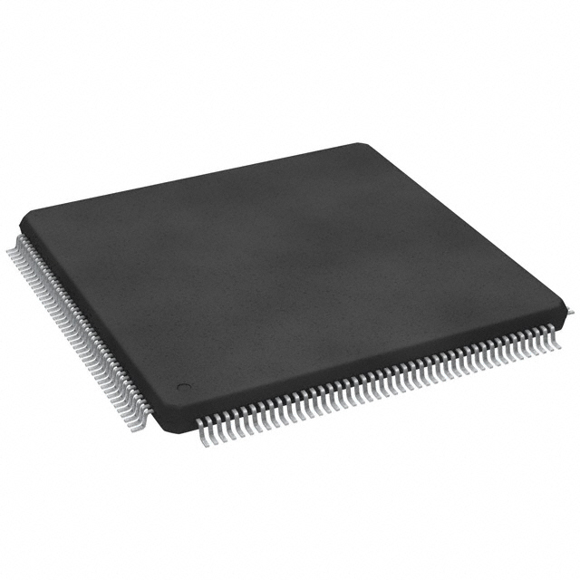
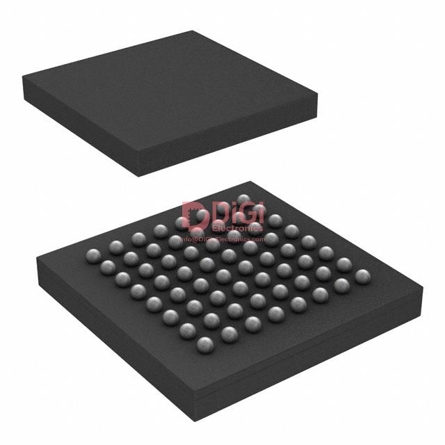
Pinout, package, and thermal management of STM32L412RBI6 STMicroelectronics
The STM32L412RBI6 leverages a compact 64-ball UFBGA package, measuring 5x5 mm with a 0.5 mm ball pitch, enabling its deployment in space-constrained and high-density applications. This geometry facilitates multi-layer PCB routing, ensuring efficient separation of high-speed and analog signals while minimizing parasitic effects. Signal distribution and ground placement are optimally allocated within the BGA matrix, which reduces EMI and supports robust high-frequency operation, particularly valuable for signal integrity in tightly routed layouts.
The pinout supports up to 52 fast I/Os, each configurable for analog, digital, or numerous alternate functions. Careful pin multiplexing maximizes available features within the limited package dimensions. The significant 5V tolerance across many I/Os provides resilience against voltage fluctuations, facilitating direct interfacing with legacy peripherals and higher-voltage sensors without requiring level shifters. This capability streamlines hardware integration and supports mixed-voltage environments, a frequent requirement in industrial and instrumentation platforms.
Mechanical characteristics, including marking specifications and recommended PCB footprints, are standardized for automated optical inspection and traceability during mass production. Recommended footprint details ensure optimal solder joint reliability and manufacturability, critical for yield in volume assembly. The body size and ball pitch are harmonized for compatibility with fine-pitch assembly processes, while clear marking schemes aid traceability throughout the supply chain.
Thermal characteristics represent a core design consideration. The package's thermal dissipation is quantified through junction-to-ambient thermal resistance parameters, serving as baseline references for power/thermal budgeting. These datasheet values, while useful for initial estimation, must be contextualized within the actual application environment. Factors such as copper layer count, via density beneath the package, and airflow govern real-world thermal paths; thus, simulation and empirical measurement remain essential before finalizing system power envelopes.
Application scenarios range from ultra-low-power wearable devices to compact industrial controllers, where thermal headroom is limited. In these contexts, distributing high-dissipation subcircuits, adopting thicker copper, and explicitly managing heat flow beneath the BGA dramatically improve margin against thermal overstress. Experience confirms that even minimal changes in board stackup or ground pad design materially affect the effective junction temperature. Proactively incorporating these optimizations—alongside the recommended land pattern—allows consistent operation, even close to specification thresholds.
A unique opportunity with this package is exploiting flexible IO mapping and robust electrical margins to build modular hardware platforms. Customizing pin assignments to suit application-specific peripherals unlocks maximum system value, while 5V-tolerant interfaces future-proof designs for evolving I/O requirements. Prioritizing careful layout, mechanical discipline, and precise thermal analysis at the engineering stage yields platforms that not only meet but extend typical application boundaries, leveraging the full potential of the STM32L412RBI6’s hardware integration.
Potential equivalent/replacement models of STM32L412RBI6 STMicroelectronics
Analyzing alternatives to the STM32L412RBI6 involves a layered examination of architectural compatibility, peripheral parity, and integration constraints within embedded system design. At the architectural level, close relatives such as the STM32L412CBI6 and STM32L412C8T6 maintain the same ARM Cortex-M4 core and low-power profile. Their memory map and system clock structures ensure deterministic porting of firmware and facilitate re-use of board-level analog front ends owing to similar I/O multiplexing. Differences in pinout, package dimension, and available flash/RAM are common points of divergence, influencing signal routing and layout density during PCB design iteration.
Beyond the immediate family, expanding to STM32L41x, STM32L43x, or STM32L44x series warrants systematic analysis of datasheet tables, focusing on subthreshold operating voltage ranges and peripheral capability deltas. These series often provide unique configurations—a wider selection of USARTs, additional low-power timers, or increased ADC channels—enabling more granular tuning of system functions under specific constraints, such as wearables with tight mW budgets or remote sensors requiring robust voltage tolerance in harsh environments. Integrating a different model into a legacy design flow frequently means re-evaluating clock source configurations and firmware abstraction layers, especially when migrating between memory densities or package outlines.
Efficient model comparison is anchored in cross-referencing not only the silicon feature sets, but also ecosystem readiness—toolchain support, HAL compatibility, and availability of proven reference designs can drastically accelerate time-to-market. Peripheral compatibility should be validated both at the register map level and via hardware abstraction, allowing optimized power-management strategies and interrupt handling routines to remain intact amid hardware substitutions. Development experience consistently shows value in prioritizing MCUs with comprehensive errata documentation and mature debug interfaces, such as support for SWD/JTAG and trace facilities, to minimize integration risk and streamline validation cycles.
Selecting the optimal replacement hinges on a multidimensional fit: balancing package constraints, functional superset availability, and projected component lifecycles. Application scenarios, whether ultra-low-power dataloggers, battery-powered sensor arrays, or industrial control nodes, benefit from a methodology that factors not just baseline specifications but the broader system-level support and peripheral synergies. Layered evaluation thus yields more robust architectural decisions and sustainable hardware platforms.
Conclusion
The STM32L412RBI6 microcontroller from STMicroelectronics integrates an advanced Cortex-M4 core, engineered for optimal efficiency in ultra-low-power embedded designs. At its foundation, the device leverages segmented power domains and multiple low-power modes, including Stop and Standby, enabling dynamic adaptation between energy consumption and system responsiveness. The architecture synchronizes clock gating with peripheral and memory management, permitting aggressive power scaling without forfeiting real-time performance—an imperative for both battery-powered and energy-scavenging environments commonly found in wearables or autonomous sensor nodes.
Peripheral interfacing is handled through a flexible interconnect matrix, supporting high-precision analog functions such as a 12-bit ADC, internal reference voltage, and programmable gain op-amp. These features underpin data acquisition tasks where accuracy, noise immunity, and minimal drift are critical, such as compact medical instrumentation or environmental monitoring nodes. The programmable analog peripherals can be directly coupled to DMA and event-driven logic—minimizing CPU intervention and reducing processing latency while extending system lifetime. Such capabilities also mitigate the classical trade-offs between performance and energy by reducing the number of required device wake-ups for event processing.
Secure provisioning and firmware integrity are increasingly vital in distributed IoT architectures. The STM32L412RBI6 addresses these needs with hardware-supported readout protection, secure boot features, and integrated cryptographic acceleration. These functionalities enable trust anchors in constrained devices, establishing device authentication and encrypted communication channels vital for industrial control, metering, or consumer security systems. Design flexibility is enhanced through embedded flash with fast write and erase cycles, supporting field firmware upgrades and secure over-the-air (OTA) updates with minimal downtime.
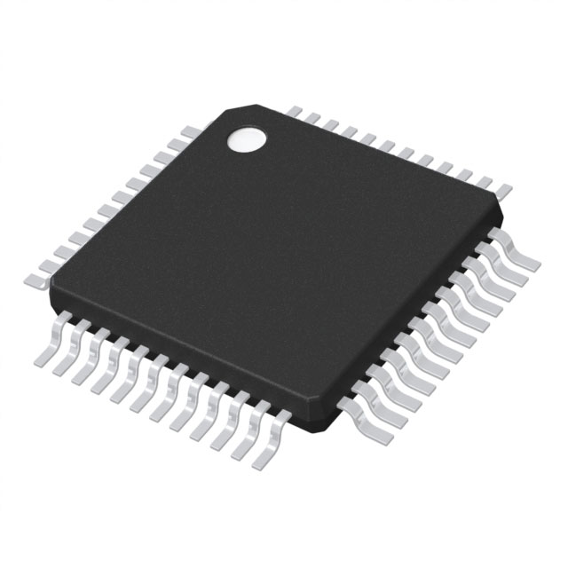
When designing for diverse communication requirements, the microcontroller’s suite of peripherals—including I2C, SPI, UART, and low-power timers—facilitates seamless interfacing with both legacy and next-generation external components. This peripheral breadth enables efficient bridging between high-speed data paths and low-bitrate control signals, streamlining integration in multiprotocol industrial gateways, smart meters, or modular instrumentation platforms. The device’s peripheral remap options and pin-rich LQFP64 package yield high PCB layout flexibility, crucial for rapid hardware iteration and pin function optimization during the prototyping phase.
Development cycles are compressed by ST’s software and hardware ecosystem, incorporating mature HAL libraries, CubeMX configuration tools, and extensive reference design repositories. Careful parameterization of the MCU’s power domains, clock trees, and peripheral interfaces during early-stage prototyping offers substantial risk reduction, enabling reproducible energy profiles and deterministic real-time operation under variable loads. Strategic partitioning of application layers—allocating signal conditioning, protocol handling, and real-time tasks to the MCU’s native accelerators—extracts maximal value from on-chip resources, minimizing external component count and bill-of-materials cost.
The STM32L412RBI6 stands out in design scenarios demanding long life, secure connectivity, and uncompromised analog fidelity. It excels where deep configurability, ready-to-use low-power techniques, and robust communication stacks drive competitive differentiation, especially in market segments where form factor, longevity, and cost/performance ratios dictate success. Informed selection and exploitation of its features can substantially elevate system reliability, simplify certification efforts, and accelerate product time-to-market.