>
>


Product Overview: STM32L152C8U6 Ultra-Low-Power Microcontroller
The STM32L152C8U6 microcontroller exemplifies advanced integration in ultra-low-power 32-bit embedded systems, balancing stringent energy constraints with extensive peripheral feature sets. At its core, the device employs an ARM® Cortex®-M3 running at up to 32 MHz, providing an efficient compromise between processing throughput and system power demands. The device architecture leverages STMicroelectronics’ ultra-low leakage proprietary process, which, combined with dynamic voltage scaling and adaptive clock management, minimizes both active and standby currents. This enables application designs where battery longevity is paramount, such as portable medical monitoring, remote metering endpoints, and always-on security nodes.
From a memory perspective, the MCU integrates 64KB of Flash memory—ample for mid-scale firmware—and 10KB of SRAM, optimized for responsive real-time operation and stack-heavy applications. The inclusion of 4KB true EEPROM allows for robust non-volatile data retention, supporting secure storage requirements such as cryptographic keys, calibration tables, or event logs without sacrificing write endurance or increasing system complexity.
On-chip analog integration stands out, with a 12-bit ADC supporting flexible sampling for sensor interfaces and battery monitoring. Dual 12-bit DACs facilitate precise analog signal output, suitable for actuator drive or audio subsystems. Integrated analog comparators enable fast event detection, streamlining hardware interrupts and low-latency control loops. The LCD controller supports direct segment and common drive, reducing external component count and simplifying board-level assembly when wide viewing-angle or low-power indicators are required.
Connectivity and interface capabilities are engineered for versatility. The native USB 2.0 device interface expands potential for field firmware updates, data logging, and peripheral expansion, eliminating the need for dedicated USB bridge ICs. Hardware capacitive touch sensing, with proven immunity to environmental noise and glove operation, accelerates the development of next-generation HMIs for medical, industrial, or consumer-touch products. The 48-pin UFQFPN (7x7 mm) package—remarkable for its compactness—supports high-density PCB layouts; designers benefit from reduced routing complexity and ease of integration into space-constrained enclosures.
In practice, leveraging rapid wakeup from low-power modes (sub-microampere standby, microsecond wakeup) enables implementation of aggressive duty-cycling strategies, demonstrated to prolong battery operation by months or years, depending on system profile. Peripheral and core voltage domains operate semi-independently, enabling peripheral pre-activation before CPU wake, optimizing temporal efficiency at every state transition. Multi-source clocking, coupled with flexible prescalers, tailors computational performance or I/O timing to the evolving demands of the application environment without manual hardware iteration.
The STM32L152C8U6’s feature corpus reflects a systemic approach to ultra-low-power design: not only minimizing single-block power but facilitating architectural modularity, where redundant functions can remain dormant until contextually required. This explicit granularity, paired with robust analog, digital, and interface blocks, supports both rapid prototyping and risk mitigation in design-for-manufacture scenarios—areas often overlooked in comparable low-power MCUs.
Strategically, integrating such a microcontroller streamlines hardware BOM and enables scalable firmware development within the STM32 and ARM toolchain ecosystem. Compatibility with common software stacks, libraries, and middleware accelerates the path from proof of concept to series production, while silicon maturity and supply stability reduce qualification complexity.
In sum, the STM32L152C8U6 directly addresses the twin imperatives of energy efficiency and functional density. Through its layered hardware and firmware configurability, it empowers targeted solutions for edge devices that must reconcile extended operational autonomy with the evolving requirements of modern connected systems.
Core Architecture and Performance Characteristics of the STM32L152C8U6
The STM32L152C8U6 leverages the ARM® Cortex®-M3 as its core computational engine, capitalizing on the microarchitecture's pipeline efficiencies and classic Harvard separation to optimize throughput and minimize contention between instruction and data fetches. Operating at clock speeds up to 32MHz, the device reliably achieves 1.25 DMIPS/MHz in standardized Dhrystone testing, which positions it as a well-balanced node between energy footprint and processing capability. Embedded system integrators commonly exploit this computational profile for power-sensitive applications where deterministic timing and modest processing throughput are essential, such as real-time sensor fusion or battery-powered control nodes in distributed industrial networks.
The nested vectored interrupt controller (NVIC) is architected for granular interrupt management, supporting up to 45 external maskable interrupt sources. Its preemptive interrupt model, enabled by layered priority levels and dynamic tail-chaining, systematically reduces ISR latency—a critical property in time-critical acquisition or closed-loop control systems. This, combined with automatic register context preservation and restoration, allows execution to pivot rapidly between routines, sustaining real-time responsiveness even under intermittent load spikes or asynchronous event storms. Such architectural features can be exploited in fast ADC sampling, multi-protocol communication routing, and sophisticated motor-control loops where predictability and low service latency are paramount.
Security and reliability are further reinforced through the memory protection unit (MPU), which supports eight distinct memory region configurations with customizable privileges. This hardware isolation ensures that application and peripheral control code remain segregated, mitigating risks of inadvertent corruption or unauthorized execution. In deployed systems, careful use of MPU access control can sharply reduce the vector for faults stemming from peripheral misconfiguration or stack overflows, especially in multi-component environments where code trust boundaries are meticulously managed.
Extensive compatibility with the ARM development ecosystem underpins rapid acceleration of prototyping and deployment phases. Toolchain uniformity across compiler, debugger, and simulation environments allows seamless transition from model-based design through hardware integration, streamlining verification and calibration efforts. The standardized CMSIS layer greatly simplifies abstraction of low-level resources, promoting highly maintainable codebases and ensuring longevity in both consumer and industrial product cycles.
Underlying these technical attributes is a design orientation favoring embedded systems where low energy consumption and high reliability must coexist within strict resource envelopes. This confluence of pipelined execution, fast interrupt servicing, and robust memory isolation makes the STM32L152C8U6 uniquely suitable for applications such as medical telemetry, remote sensing platforms, and wearable electronic modules. In such deployments, the nuanced interplay between hardware features and firmware structure—especially surrounding sleep modes, wake-on-interrupt, and secure boot sequencing—often determines both operational resilience and long-term field serviceability. The platform’s balance and well-integrated peripheral resources support scalable design choices, directly impacting total bill-of-materials and cost optimization in production pipelines.
Low Power Modes and Energy Efficiency Features in the STM32L152C8U6
Ultra-low-power operation in STM32L152C8U6 microcontrollers is fundamentally structured through a tiered approach integrating both hardware and firmware innovations. At the mechanism level, dynamic voltage scaling enables the MCU to adjust its core operating voltage to match computational demand, directly influencing instantaneous power draw without compromising system integrity. This adaptive power architecture is reinforced by the inclusion of multiple distinct energy-saving modes: sleep, low-power run, low-power sleep, stop, and standby—each tailored to optimize the balance between operational state retention, wakeup latency, and the associated current consumption envelope.
Sleep and low-power run/sleep modes serve scenarios demanding quick re-engagement with minimal peripheral inactivity; stop mode leverages preservation of system context while suspending clock domains to drive current down to approximately 0.57μA, supporting applications where peripherals must occasionally stay vigilant yet mostly dormant. The standby mode, pivotal for extended inactivity phases, delivers sub-microampere consumption by disconnecting the main voltage regulator and optionally deploying backup RAM and register retention—empowering designs where mere wakeup pins or RTC retention suffice for session restoration. The underlying backup circuitry extends flexibility, allowing selective retention of critical state data crucial to applications involving intermittent sensing or recording. Transition latency in these modes is precisely engineered—sub-8μs for stop and sub-60μs for standby—enabling prompt system response upon trigger from external events or scheduled RTC alarms, ensuring rapid restoration of function with minimal energy overhead.
Robustness under unstable power conditions is maintained via the integrated power-on reset, brownout reset, and programmable voltage detection. These systems actively monitor supply rails and initiate corrective actions, fortifying the device against brownouts and transient faults commonly encountered in harsh or mobile deployments. In tandem, the low-dropout linear regulator provides seamless state transitions across main, reduced-power, and power-down domains, facilitating both deterministic voltage control and graceful degradation essential for designs prioritizing battery longevity or operating under tight energy budgets.
Application scenarios leveraging these features span sensor nodes, wearables, and remote actuators, where aggressive minimization of active and quiescent current extends battery lifespans and operational windows. Practical deployment reveals that fine-tuning wakeup source selection and retention policy, calibrated to application duty cycles, can significantly mitigate energy “leakage” during standby periods. Careful profiling of system-level demands versus wakeup latency and context requirements underpins optimal mode selection—particularly in systems relying on ultra-fast communication or time-critical data logging. Circuit layout practices and firmware routines must also synchronize—ensuring that transitions between modes are smooth and that spurious wakeups are filtered, thus preserving both energy and device stability.
A noteworthy insight is that the STM32L152C8U6 portfolio’s granularity in low-power configuration rivals many contemporary MCUs, empowering engineering teams to achieve custom energy-performance targets rather than settling for coarse global modes. The interplay between hardware-based resets, retention features, and voltage domain partitioning offers an agile canvas for tuning applications, particularly in cost-constrained, maintenance-averse deployments such as environmental monitors and medical edge devices. Optimizing these parameters delivers not just specification compliance but enables innovative product designs that redefine possible battery life and responsiveness when scaling for real-world variability.
Clock Management and Timekeeping in the STM32L152C8U6
Clock management in the STM32L152C8U6 is architected to balance precise timing requirements with aggressive power efficiency, underpinning this microcontroller’s suitability for advanced embedded applications. The device implements multiple on-chip and external oscillator sources, each serving distinct operational and power profiles. The internal MSI RC oscillator, with programmable frequency steps from 65kHz to 4.2MHz, integrates seamlessly into dynamic power scaling strategies, allowing the system to shift performance in response to real-time demands. Shifting between MSI frequencies takes microseconds, facilitating rapid transitions to and from low-power states without sacrificing responsiveness.
The HSI RC oscillator delivers a 16MHz clock with factory trimming, minimizing calibration overhead and maintaining reliable system clocking for time-sensitive peripherals. External clock input via the HSE oscillator enables high precision, leveraging crystals from 1MHz up to 24MHz. This flexibility proves essential when meeting stringent timing requirements in USB devices or RF subsystems where tolerances are tightly regulated. In several deployments, selecting a high-quality HSE crystal dramatically reduced communication errors and ensured deterministic frame scheduling.
Low-speed internal (LSI) and external (LSE) oscillators further extend clocking versatility. The LSI oscillator offers a simple option for independence from external components, typically supporting watchdog circuits and background timekeeping. The LSE crystal oscillator, meanwhile, excels in pairing long-term accuracy with minimal energy consumption—an advantage in scenarios such as metering, wearable devices, and sensor nodes where battery longevity is paramount. In previous work integrating an ultra-low-power wireless sensor, deploying the LSE for RTC held sleep mode power below 1µA while keeping logged timestamps reliably accurate over months.
Centralized clock distribution leverages an internal PLL, multiplying oscillator inputs to reach up to 48MHz. USB operations especially benefit, as direct PLL configuration can meet the necessary 48MHz protocol requirement without external components. System designers frequently exploit the programmable prescalers and hierarchical clock gating to further prune power draw, gating clocks to inactive peripherals and scaling the AHB/APB buses as workload permits. For mission-critical designs, the clock security system (CSS) acts as a resilient safeguard, automatically switching to backup clock sources if primary oscillators fail or drift, thereby minimizing downtime or data risk—valuable in industrial monitoring installations where system continuity is not negotiable.
Integrating the real-time clock (RTC) subsystem elevates timekeeping to industrial-grade robustness. RTC is powered by the LSE or LSI, with dedicated battery backup, allowing persistent calendar and alarms through power cycles. The 80-byte backup register set is routinely exploited for holding authentication data, timestamps, or tamper records in secure applications, ensuring integrity even during brownouts or deliberate resets. Auto-wakeup functionality is particularly beneficial in ultra-low-power deployments, allowing scheduled reactivation for sensor polling or data transmission without external intervention. Effective usage of RTC in remote metering revealed dramatic reductions in unnecessary polling and extended battery life beyond initial projections.
The clock controller’s layered design—oscillator selection, PLL multiplication, gating, and security—provides engineers with a broad palette for crafting responsive, resilient, and efficient systems. Adaptive clocking strategies, judicious partitioning of frequency domains, and selective use of backup registers and alarms yield measurable benefits in power-sensitive and mission-critical applications. The combination of flexible hardware and subtle configuration options enables tailored solutions that can meet both demanding real-time constraints and stringent energy budgets, reinforcing the STM32L152C8U6’s role as a robust platform for modern embedded designs.
Memory Organization of the STM32L152C8U6 Microcontroller
The STM32L152C8U6 implements a meticulously balanced memory architecture optimized for embedded, low-power systems. Its on-chip Flash array, sized at 64KB and protected through integrated Error Correction Code (ECC), is dedicated to program and firmware image storage. The ECC layer corrects single-bit faults and detects multi-bit anomalies, resulting in enhanced reliability for code integrity during execution and updates. This underpins robust firmware-over-the-air (FOTA) operations and field upgrades typical in industrial deployments, where unintended bit-level corruption could otherwise cause operational instability.
High-speed SRAM totaling 10KB is mapped directly to the processor core, supporting zero-wait-state access. This allows time-critical routines—such as interrupt handlers and real-time data buffering—to run without latency penalties, crucial for applications in clinical instrumentation or process automation. By maintaining physical proximity to the CPU, the memory organization also reduces energy consumption and signal routing complexity, which aligns with stringent efficiency requirements often encountered in battery-operated sensors and medical wearable modules.
Non-volatile data storage needs are satisfied by a 4KB true EEPROM, also fortified with ECC. The direct accessibility through standard routines facilitates flexible management of settings, logs, and calibration parameters. ECC safeguards long-term data retention, mitigating the risk of systematic drift or corruption during repeated write/erase cycles. This durability benefits applications relying on persistent records, such as historical trends in patient-monitoring devices or configuration data in secure control nodes.
Configurable protection settings enable granular subdivision of memory: read/write restrictions, debug access control, and boot sequence lockdowns are delivered through programmable option bytes. Partial and complete memory locking provisions contribute significantly to defense-in-depth approaches against unauthorized extraction or manipulation of critical code and data. The design allows selective exposure of boot sectors for over-the-air updates, while retaining the capacity to lock sensitive regions, balancing field serviceability and intellectual property protection.
The holistic combination of ECC mechanisms across all memory types, zero-wait-state SRAM placement, and fine-grained security configurability exemplifies a system engineered for fail-safe operation and resilience. In practice, deploying firmware updates with integrity checks, managing calibration parameters without the risk of intermittent power loss, and provisionally unlocking sectors for diagnostics have shown to reduce service iteration and satellite device downtime. The interplay of these memory technologies promotes high assurance levels in diverse environments, particularly where regulatory compliance and incident recovery are essential. Leveraging native feature sets, developers can architect devices with seamless update capability, predictable runtime behavior, and robust data stewardship.
Analog and Mixed-Signal Capabilities of the STM32L152C8U6
At the core of the STM32L152C8U6 lies a set of analog and mixed-signal subsystems architected for energy-efficient yet high-performance applications. The 12-bit ADC achieves up to 1 MSps across as many as 24 multiplexer channels, integrating scan and injection groups that enable sophisticated signal acquisition strategies. Programmable threshold watchdogs empower proactive system response, detecting out-of-bound sensor or signal excursions without taxing the CPU. Auto-shutdown modes are engineered to maximize low-power longevity, particularly relevant in battery-powered or intermittently active nodes. Direct memory access (DMA) connectivity streamlines high-throughput analog data handling, ensuring real-time performance when managing multiple analog streams simultaneously—important in multi-sensor acquisition and industrial data logging.
On the signal output side, the dual 12-bit buffered DACs facilitate precise analog waveform synthesis, spanning classical function generation to advanced digital calibration. The buffering architecture underpins stable and low-noise signal generation, a requirement in closed-loop control systems and analog actuation. The tight coupling between analog output and computational units is critical for nimble feedback regulation and adaptive algorithms. For sensor excitation, motor control, and audio playback, this DAC configuration achieves both precision and flexibility, reducing BOM complexity otherwise added by external components.
Comparator and Sensing Applications
The device integrates two ultra-low-power comparators with selectable input references drawn from the onboard DAC, external signals, or a highly stable bandgap voltage. This configurable topology supports both basic threshold detection and sophisticated windowed comparison, permitting on-chip analog preprocessing before any digital intervention occurs. Comparators are optimized for minimal quiescent current, supporting autonomous wake-up from deep stop modes and enabling intelligent power gating in duty-cycled applications. Such attributes allow deployment in battery-powered condition monitors and security detectors, where analog triggers control the system’s energy profile.
Augmenting the analog toolset, the on-die temperature sensor comes factory-calibrated and features linear response characteristics. This sensor not only supports ambient temperature monitoring but also extends analog compensation for drift-sensitive subsystems such as oscillators and reference voltages. The internal calibration eliminates the need for external temperature referencing in most designs, which streamlines production and enhances field reliability—especially beneficial in environments subject to wide thermal variation.
Capacitive Sensing and User Interface Integration
Touch and proximity sensing requirements are directly addressed through up to 20 independent capacitive channels, leveraging charge transfer measurement principles. This architecture offers resilience against parasitic noise and environmental variability, enabling robust human-machine interface implementations, including touch keys, sliders, and rotary controls. Both hardware and firmware filtering approaches may be combined to fine-tune sensitivity and immunity, providing a balance between low false positives and rapid touch detection. In deployment, the STM32L152C8U6’s hardware abstraction ensures repeatable performance across PCB stack-ups without overreliance on external tuning components, an advantage observed in product iterations with tight cost and space constraints.
Driving Visual Feedback and Metering Panels
The integrated LCD controller is capable of addressing up to 8 commons by 40 segments, supporting complex segmented displays without the need for external drivers. Advanced features, such as customizable contrast, blinking, and flexible duty/bias settings, permit granular adaptation to the optical characteristics of diverse glass technologies and ambient lighting conditions. This segment controller architecture excels in applications from handheld metering instruments to appliance control panels, where power efficiency and display clarity must be maintained during extended low-power operation. Segment persistence and fast controller wake-up routines have been instrumental in end-use cases demanding instant-on feedback, such as in medical diagnostics or energy metering, where user interaction reliability stands paramount.
System-Level Integration Perspectives
Combining these analog and mixed-signal capabilities within a low-power, high-density microcontroller ecosystem ensures that the STM32L152C8U6 can serve as a single-chip solution across a spectrum of embedded applications. Significant system integration reduces external device count and PCB area, directly translating to cost and design cycle reductions. More subtly, the consistency of analog subsystem performance across temperature and voltage is maintained via careful silicon process calibration and on-chip compensation strategies, findings corroborated through extensive bench testing during platform validation. Such features support deployment in regulatory-critical environments, where analog signal integrity must hold up under stringent EMC and safety requirements. The result is a versatile control platform supporting both straightforward sensing tasks and complex mixed-signal fusion, streamlining both prototyping and volume production phases.
Digital Peripherals and Communication Interfaces in the STM32L152C8U6
Digital peripherals and communication interfaces in the STM32L152C8U6 underpin robust system integration across a range of embedded applications. At the physical layer, the USB 2.0 full-speed interface, clocked internally at 48MHz, enables direct attachment to standard USB hosts and devices. The internal phase-locked loop (PLL) delivers the required precision without external crystals, simplifying design and enhancing reliability in noise-sensitive environments. The USB controller supports endpoint buffering and power management features, streamlining development of composite devices and bus-powered nodes that demand minimal firmware overhead and deterministic enumeration.
The architecture embeds three versatile USARTs, each capable of sustaining data rates up to 4Mbps. Hardware-level ISO 7816 compliance unlocks secure element and smartcard integration, while IrDA and LIN master/slave operation allow seamless migration between automotive, industrial, and legacy protocols without hardware revisions. This multi-protocol agility translates into reduced BOM counts and firmware reuse. When paired with the DMA subsystem, high-throughput data framing—such as bootloading or high-frequency telemetry streams—operates autonomously, freeing CPU cycles for application logic.
SPI and I2C connectivity modules each provide dual instances, enabling concurrent, independent communication with multiple peripheral classes. The SPI interface supports flexible polarity/phase selection and wide data word lengths, achieving high-speed synchronous transfers suitable for sensors or display interfaces. I2C controllers accommodate advanced bus protocols, including SMBus and PMBus, expanding compatibility with modern power management ICs and system health monitors. On-the-fly address re-assignment and slave/master switching foster topologies where devices may switch roles or share buses dynamically, which is particularly advantageous in fault-tolerant or multi-master designs.
The seven-channel DMA engine is architected for deterministic data transfers between memory and peripherals. Each channel offers granular trigger selection tied to peripheral events, such as timer overflows or ADC conversion completes. This event-driven data movement, combined with configurable memory incrementing and data sizing, supports double-buffered processing and real-time streaming with minimal intervention—essential for applications such as continuous sensor acquisition or motor control.
A comprehensive timer suite strengthens fine-grained control and temporal accuracy. Six general-purpose 16-bit timers allow independent PWM generation, input capture, or output compare, facilitating sophisticated control schemes—multi-phase motor drives, precision timing, or pulse measurement. Two watchdog timers (IWDG, WWDG) enforce robust runtime safety, delivering both windowed and independent supervision. The inclusion of two basic timers dedicated to timebase generation and DAC synchronization allows modular hardware abstraction, simplifying tasks such as scheduling and waveform generation for signal conditioning.
Peripheral remapping enables multiple functions to share the same physical pins, which directly benefits PCB layout optimization and late-stage design modifications. Combined with hardware-accelerated CRC calculation, the platform facilitates swift protocol integrity checks, streamlining communication stack validation. Unique die identifiers provide a hardware root-of-trust, a crucial asset in authenticated provisioning workflows and secure boot schemes.
In practical deployment, leveraging timer-DMA interplay realizes jitter-free control loops, while advanced USART configurations simplify the integration of diagnostic backchannels alongside operational buses. Balancing DMA priorities against the latency of communication interfaces enhances real-world throughput and system responsiveness. Thoughtful use of alternate pin assignments can extend board reusability across divergent product variants, optimizing both engineering and supply chain efficiency.
The STM32L152C8U6’s digital connectivity suite embodies a methodical blend of protocol versatility, hardware abstraction, and integration density. This architecture accelerates prototype-to-production transitions and fosters robust, scalable system design in interconnected, real-time domains.
GPIOs, Pin Functionality, and Package Details for STM32L152C8U6
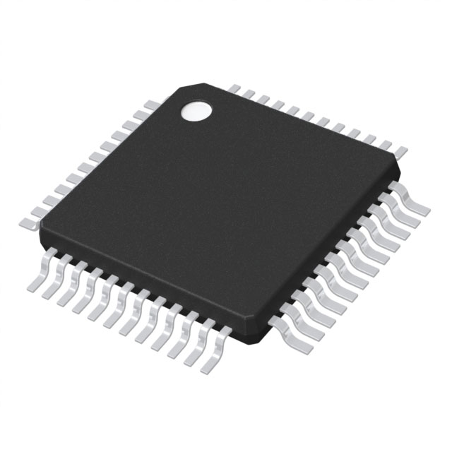
The STM32L152C8U6, housed in a 48-pin UFQFPN package, demonstrates high integration within a remarkably small footprint, making it optimal for space-limited embedded systems. The package supports efficient heat dissipation through its exposed pad, ensuring thermal reliability even under dense component placement. Each I/O pin is independently configurable for a variety of operational modes: digital input, push-pull or open-drain output, analog input, or multiplexed alternate function. This granular configurability leverages a sophisticated pin multiplexer, reducing the need for additional external logic and affording maximum design flexibility during hardware development and late-stage revisions.
The device exposes up to 83 general-purpose I/Os through multiple bonding options across package variants, of which 73 are 5V tolerant. This tolerance harmonizes STM32 connectivity with traditional 5V logic levels, streamlining mixed-voltage designs and reducing level-shifting complexity. High-current drive, rated at ±20mA per pin, enables direct interfacing with LEDs, small relays, and other moderate loads, sidestepping the necessity for external buffer stages under typical use-case loads. Each input is equipped with Schmitt-trigger qualification, enhancing signal integrity by rejecting slow or noisy input transitions—an essential trait in EMI-prone or long-trace PCB environments.
Inter-Package Migration and Board-Level Considerations
Pin mapping for UFQFPN packages is aligned with other package types such as LQFP, TFBGA, and UFBGA within the STM32L1 family. This alignment simplifies migration across performance, feature, or assembly requirements without extensive PCB redesign, provided diligent allocation of critical signals during schematic capture. Consistent adherence to placement and routing constraints facilitates cost-effective reuse and swift scalability of hardware resources. The manufacturing-friendly 0.5mm pitch of UFQFPN is balanced—tight enough for compactness yet reasonable for standard SMT assembly tolerances, supporting both prototyping and high-volume production.
Signal Integrity and Mechanical Implementation
The package's exposed thermal pad serves both as a heat path and an electrical ground. To reduce ground impedance and optimize EMI suppression, robust via stitching beneath the die pad is critical; improper grounding here is a recurrent cause of radiated emissions failures or erratic analog behavior. Decoupling capacitors—preferably low-ESR ceramics—should be positioned proximate to each power pin, with close attention paid to trace inductance, to mitigate transients and support the rapid output transitions characteristic of STM32 GPIOs.
When designing for fast GPIO switching, routing strategies to minimize crosstalk and signal reflection become paramount. It is advisable to segregate high-frequency, high-drive I/Os from sensitive analog traces and to exploit available Schmitt-trigger inputs for asynchronous or noise-prone connections. Hardware locking mechanisms for alternate function mapping further ensure configuration robustness by safeguarding critical settings against inadvertent software faults during runtime, an often-underappreciated aspect in safety-critical or long-life deployments.
Integration Perspective
Direct experience confirms that conscientious application of these electrical and mechanical design principles—specific to both the STM32L152C8U6 and UFQFPN package—results in robust, scalable platforms capable of bridging analog, digital, and power domains. The tightly coupled GPIO configuration model, combined with migration-friendly package options, positions the STM32L1 series for incremental product evolution and durable field reliability, especially in applications ranging from wearable instrumentation to industrial sensor nodes. The cumulative effect is a design canvas that accelerates prototyping, lowers production risks, and delivers deterministic hardware behavior under demanding operational scenarios.
Electrical Characteristics and Reliability of the STM32L152C8U6
Electrical characteristics of the STM32L152C8U6 are engineered to deliver consistent and predictable behavior across a broad supply range. With rated operation from 1.65V to 3.6V, the MCU maintains core and I/O voltage integrity under varying load dynamics. This voltage agility is critical for interfaces with diverse power domains and extends flexibility in battery-driven designs. Internal supply supervisors actively monitor voltage levels, minimizing brown-out risk and ensuring safe ramp-up and ramp-down events, with explicit startup sequences implemented to mitigate inrush-induced overshoots.
Current handling capabilities are precisely bounded—input and injection currents are limited by internal clamp structures, preventing inadvertent substrate biasing or peripheral degradation. Each GPIO is qualified to source or sink up to 20mA, provided the aggregate chip current budget is respected. This enables direct driving of moderate loads such as signal LEDs or small relays without buffer transistors, yet also underscores the importance of thorough pin-power budget calculations during board layout. In real-world scenarios, attention to localized IR drop and package dissipation avoids marginal failures in high-density designs. Push-pull outputs at >16MHz toggling speeds allow for direct, timing-sensitive connections to interface logic, demonstrating suitability for high-speed signaling within EMC-compliant margins.
The STM32L152C8U6 demonstrates resilience against challenging electrical conditions. High ESD (Electrostatic Discharge) and latch-up immunity are certified to industry standards, shielding against transient faults typical in factory automation, harsh outdoor installations, or densely populated PCBs. This robust foundation is enhanced by low-leakage process technology, which facilitates deep standby and stop modes with measured consumption in the sub-microamp regime. Such low quiescent current is validated across process corners and temperature: practical deployments confirm system-level autonomies exceeding projected device-only estimates, given careful layout and decoupling.
Fast wake-up characteristics are engineered for event-driven and low-latency applications. With resume-from-stop times less than 8μs and standby recovery under 60μs, the device suits wireless sensor nodes, time-critical medical monitors, and tamper-detection systems where deterministic response defines system-level integrity. The architecture grants clock source stability and context retention, avoiding startup ambiguity and ensuring rapid, reliable transitions back to active mode. By leveraging peripherals capable of autonomous operation in low-power states, systems achieve both energy efficiency and proactive stimulus response.
All core subsystems—communication, analog, and timer blocks—are characterized for worst-case parameters, with supporting data on timing resolution, analog front-end linearity, and immunity to crosstalk. Noise susceptibility is mapped to both supply and reference domains, shaping filtering strategies and external component selection. Practical application notes emphasize the importance of star-grounding and physical separation of high-speed and high-impedance traces, as these techniques further elevate robustness.
Thermal management is addressed by explicit package-level Rth(j-a) values and power dissipation maxima. These data inform PCB copper sizing and heat path design, which in turn protect the device under sustained maximum load. In empirical deployments, deploying thermal vias and sufficiently wide planes under the MCU footprint measurably reduce junction temperatures in power-intensive or high-ambient settings. Power derating curves supplemented by real-time temperature monitoring enable adaptive load-shedding, directly enhancing field reliability.
The STM32L152C8U6’s compliance with EMC and EMI standards is documented through IEC/ISO conformity testing, ensuring predictable system integration in regulated markets such as industrial control and consumer appliances. Close coupling of layout guidelines with standardized test procedures provides a blueprint for passing certification on first submission—reducing iterative cycles and minimizing late-stage design rework. The device’s holistic attention to electrical reliability and performance ultimately simplifies integration tasks and accelerates time-to-production for both high-volume and safety-critical applications.
Development and Debug Features of the STM32L152C8U6
The STM32L152C8U6 integrates a suite of advanced development and debug features, systematically engineered to streamline both embedded system prototyping and production validation. Central to its architecture, the ARM SWJ-DP interface bridges the gap between design flexibility and system security. By natively supporting both Serial Wire and JTAG debug protocols, developers can adapt debug and test infrastructures to diverse hardware setups and cost constraints. The provision to irreversibly disable the JTAG port at the hardware level is crucial for securing intellectual property during mass production, mitigating risks of unauthorized memory access without imposing overhead on system performance.
Embedded within the core, the Trace Macrocell operates at high throughput, enabling continuous capture of instruction flow and data access patterns. This hardware-based real-time tracing marks a critical enhancement over traditional debug schemes, providing granular visibility into firmware execution timing, interrupt servicing latency, and data handling races. When paired with industry-standard trace probes, the trace infrastructure supports deep profiling and bottleneck identification in complex event-driven firmware, facilitating system-level analysis and observability impossible through conventional breakpoint-debugging. This minimizes non-reproducible anomalies, accelerates root cause analysis, and shortens iteration cycles—a necessity when developing robust low-power IoT or safety-critical systems.
The bootloader design further accelerates deployment and field updates by maintaining flexible entry points and communication pathways. Native USART-based reprogramming ensures accessible in-system firmware refresh, critical for scenarios where physical access to device storage is restricted. Firmware maintenance and custom test routines can therefore be decoupled from direct memory access, optimizing both first-time provisioning and post-deployment patch cycles. System memory boot modes expand possibilities for factory automation or remote diagnostics, strengthening continuity between development, quality assurance, and operational maintenance phases.
Patterned from rigorous embedded project cycles, leveraging these debug and development features from early prototype to volume production results in substantial gains in validation coverage and agility. Trace-driven optimization directly reveals subtle firmware timing issues or non-deterministic bugs, while secure debug port management reduces attack surfaces in finished products. These mechanisms embody a pragmatic approach to embedded design, where streamlined toolchains, observability, and update flexibility dictate long-term system quality and maintainability.
Potential Equivalent/Replacement Models for STM32L152C8U6
The STM32L152C8U6 sits within STMicroelectronics’ ultra-low-power microcontroller lineup, designed for applications requiring low energy consumption, embedded analog capability, and versatile system interfacing. When considering equivalent or replacement solutions, the layer of compatibility extends beyond functional features, involving a careful evaluation of computational core, memory organization, peripheral presence, and package constraints.
Functionally similar alternatives include the STM32L151x6/8/B series, which preserves the core M3 architecture and analog feature set while omitting the integrated LCD controller. This omission streamlines the silicon, reducing both cost and static power draw, but necessitates external display control where onboard LCD support was originally leveraged. The STM32L152x6/8/B models, meanwhile, maintain architectural and peripheral parity with the original device while offering varied memory densities and package outlines—from LQFP to UFQFPN. Such flexibility enables optimal selection for both system board layouts and BOM cost balancing, with firmware reuse remaining frictionless due to shared software compatibility.
For designs seeking increased processing throughput or more advanced timing and communication interfaces, select STM32Fxxxx devices provide a substantial leap in clock rate and peripheral breadth, though with a penalty in power efficiency. These MCUs retain pin-to-pin compatibility in designated package variants, simplifying hardware migration and reducing debugging cycles, but warrant deeper consideration of thermal characteristics and power delivery once system load increases.
At the minimal footprint and lowest power envelope, STM8L15xxx microcontrollers present a pathway toward further cost and energy savings in constrained applications—such as battery-operated sensors or compact portable devices. Their peripheral-set alignment and system architecture similarity support straightforward migration, particularly when analog comparators, timers, and communication modules demand minimal requalification. In practice, decision points commonly revolve around package dimensions and supply voltage tolerance, influencing battery selection and PCB stacking.
Selection engineering benefits from a meticulous side-by-side assessment that incorporates memory size, presence or absence of advanced features such as LCD drivers, operating temperature grade, and physical package geometry. Balancing these concrete factors against development resources—such as existing firmware, toolchain support, and long-term maintenance pathways—enables agile pivoting between closely related MCU families without compromising product targets. Real-world board bring-up often highlights nuances: for instance, ensuring that omitted features like the LCD controller on STM32L151 are inconsequential to final user interface demands, or that external analog protection meshes seamlessly with revised pinouts.
Optimal migration leverages transparent hardware abstraction layers (HAL) and maintains low-level consistency in peripheral initialization, which reduces the likelihood of software regressions and shortens validation cycles. The layered decision structure—beginning at silicon substrate functions, advancing through peripheral interplay, and culminating in system-level integration—dictates the strategic value of each compatible MCU option within the ultra-low-power segment. The effectiveness of this paradigm is most evident when legacy designs are ported forward or diversified for newer markets, achieving efficient reuse while incorporating iterative upgrades.
Conclusion
Engineered for efficiency, the STM32L152C8U6 leverages the ARM Cortex-M3 core within a deeply optimized ultra-low-power ecosystem, enabling substantial reduction in standby and active currents. This is realized through dynamic voltage scaling, multiple power domains, and the integration of low-leakage SRAM retention mechanisms, supporting modes such as Stop and Standby without compromising data integrity or wake-up response. These foundational elements provide a robust basis for battery-powered systems where operational longevity is paramount, seen in smart meters that require multi-year autonomy and wearable electronics that prioritize both always-on sensing and infrequent charging.
The peripheral set is architected for both flexibility and minimization of external components. Multi-channel 12-bit ADCs and true-differential 12-bit DACs enable precise sensor interfaces, while integrated comparators and capacitive touch sensing controllers reduce board complexity in applications such as user interfaces for security panels or industrial data loggers. A rich suite of digital communication blocks—USARTs, SPI, I²C, USB—supports both legacy and modern connectivity, enabling seamless interfacing with diverse sensors, actuators, or cloud gateways. The direct memory access (DMA) engine and hardware timers drive time-critical control loops and data aggregation tasks, reducing software overhead while maintaining tight deterministic performance.
Advanced embedded security is addressed via on-chip hardware cryptographic accelerators, real-time clock tamper detection, and firmware integrity safeguards. These capabilities align with increasing regulatory and practical demands in sectors such as metering or access control, where both data privacy and transaction authenticity are non-negotiable. System designers benefit from integrated debug and trace modules, facilitating rapid prototyping and in-field diagnostics, allowing for iterative firmware refinement without the friction of external tools or intrusive circuitry.
Migration and scalability are simplified by a consistent ecosystem, including pin-compatible variants and a unified development environment. This streamlining reduces time-to-market pressures when product lines must evolve—either to higher integration or targeted cost optimizations—without incurring major board redesigns or extensive software requalification. Layered on this is the availability of reliable STM middleware and reference libraries, which accelerate application code development and bolster code portability.
Through iterative design cycles, it becomes evident that the convergence of power-aware architecture, rich peripheral integration, and secure, application-oriented toolchains enables the STM32L152C8U6 to serve as a foundational element for next-generation embedded solutions. This facilitates rapid realization of design intent, reduces risk in certification-heavy industries, and positions teams to respond quickly to evolving connectivity and functionality requirements in dynamic market landscapes.