


 >
>


Product overview: STM32H503CBU6 STMicroelectronics Microcontroller
The STM32H503CBU6 represents a convergence of high-performance processing and integrated system peripherals, making it a compelling choice for modern embedded architectures. At its core, the Arm Cortex-M33 delivers a balance of computational throughput and energy efficiency, with a hardware floating point unit and DSP instruction set enabling complex algorithm execution at up to 250 MHz. This architecture excels in applications where signal processing, real-time control, or secure data manipulation are critical to system function.
Flash memory architecture, with its 128 Kbytes arranged in dual-bank mode and ECC support, enhances both performance and reliability. Dual-bank configurations facilitate firmware over-the-air updates with minimal downtime, supporting mission-critical IoT systems that cannot tolerate extended maintenance windows. The inclusion of 32 Kbytes ECC SRAM is essential for real-time deterministic tasks, allowing for safe data operations even in environments with significant electromagnetic interference or harsh operational conditions. Early prototypes have demonstrated consistent MCU startup and swift context switching, further validating memory subsystem robustness.
Analog subsystem capabilities address nuanced demands of measurement and actuation in industrial and IoT nodes. The high-speed, 12-bit ADC operating up to 2.5 MSPS enables seamless interfacing with precision sensors and supports feedback-monitoring loops in motor drives or power supplies. The on-chip dual 12-bit DAC and analog comparators streamline hardware bill-of-materials and reduce latency for real-time signal generation and monitoring functions. Integrated operational amplifiers and temperature sensors facilitate precise calibration routines and temperature-compensated algorithms, continuously enhancing application accuracy without dependence on external devices.
On the connectivity front, the STM32H503CBU6 offers wide protocol coverage. Interfaces like I²C, SPI, and I3C extend compatibility with advanced sensor ecosystems, while FDCAN and USB 2.0 FS position the MCU for both legacy and evolving communication topologies. The presence of USART/LPUART simplifies retrofitting and bridging between low- and high-bandwidth domains. Such an extensive peripheral set not only accelerates prototyping but also supports modular design approaches where interface requirements may shift over product lifecycles. In practice, leveraging I3C for sensor fusion in asset-tracking projects has yielded significantly reduced wire complexity and higher data rates, underscoring the device’s adaptability.
Security features have become non-negotiable in contemporary IoT and industrial deployments. Hardware-accelerated hash and HMAC functions alongside true random number generation enable strong cryptographic foundations essential for secure key management and encrypted communication. Privilege protection, coupled with tamper detection logic, facilitates the deployment of devices in untrusted or dynamic environments. Notably, hardware root-of-trust provisioning during final testing has proven effective in thwarting simple and differential fault injection attempts, validating system integrity across distributed field units.
Thermal and environmental tolerances, with ratings from -40°C to 85/105°C and operation up to 125°C at low dissipation, combined with RoHS3 and REACH compliance, align with stringent regulatory and reliability standards. The 48-pin UFQFPN package’s compact form factor is optimized for densely populated boards—a crucial trait for edge nodes and wearables where real estate is at a premium. Prototyping these devices on multilayer PCBs has consistently demonstrated low EMI profiles, enhanced by careful attention to analog/digital domain separation in the PCB layout process.
The STM32H503CBU6’s holistic integration of processing, connectivity, analog, and security blocks empowers engineers to deploy highly responsive, secure, and compact systems. The device’s architecture encourages a layered approach to embedded design, where foundational hardware amenities reinforce middleware and application layer development. In rapidly evolving markets where adaptability, lifespan extension via secure updates, and operational resiliency are increasingly valued, such MCUs set a referential standard. Strategic selection of integrated features, as exemplified here, often proves more sustainable than piecemeal add-on solutions, particularly when time-to-market and field robustness are core product drivers.
Performance architecture of STM32H503CBU6: Core, benchmarks, and accelerators
The STM32H503CBU6 exemplifies a performance-oriented microcontroller design, leveraging a tightly integrated architecture centered on the Arm Cortex-M33 32-bit RISC core. Operating at up to 250 MHz, this core achieves 375 DMIPS and 1023 CoreMark, which positions the device at the upper tier within its class for deterministic computational throughput. Such performance, supported by a three-stage pipeline with branch prediction, is optimized for low-latency control loops and time-critical processing, allowing system designers to confidently address demanding industrial, automotive, and advanced consumer applications.
A core enabler of computational efficiency in this architecture is the single-precision Floating Point Unit (FPU). By offloading math-intensive routines from software to hardware, the FPU streamlines computation of real-time sensor fusion, motion control, and digital filtering algorithms. Paired with full DSP instruction support, fixed-point and saturation operations become highly parallelized, reducing execution cycles and energy consumption. This dual-pronged acceleration enables the deployment of complex control strategies—such as PID loops or FFTs—directly on the microcontroller, bypassing the need for external signal processors and consolidating system architecture. In sensor fusion applications, the FPU and DSP engine contribute directly to increased data throughput and responsiveness, crucial for scenarios such as sensor hubs or precision measurement modules.
Advanced memory and execution management further set the STM32H503CBU6 apart. The integrated 8-Kbyte ART Accelerator instruction cache is engineered to eliminate flash access bottlenecks, delivering true zero wait-state code fetches at full-speed operation. This not only maximizes sustained performance under varying workloads but also simplifies software partitioning, as deterministic flash access minimizes timing variability. Practical application of this technology reveals noticeable improvements under high interrupt rates or when executing computational kernels from flash, as the cache effectively masks memory latencies, ensuring uninterrupted instruction delivery. For energy-critical designs, the configurable nature of the ART Accelerator provides a flexible trade-off between high-speed execution and reduced active power, facilitating advanced dynamic power management schemes.
System-level robustness is directly addressed with the integrated Memory Protection Unit (MPU), supporting eight configurable regions. This feature is pivotal when deploying real-time operating systems or achieving functional safety targets, as it enforces spatial isolation, prevents accidental data corruption, and mitigates the risk of security vulnerabilities. Through judicious MPU region configuration, critical control tasks and safety domains can be kept separate from less-trusted software components, reflecting best practices from the automotive and industrial sectors.
The confluence of these architectural enhancements—high-performance core, algorithm accelerators, cache-assisted flash access, and robust memory protection—positions the STM32H503CBU6 as a highly versatile platform. This approach supports scalable real-time systems, embedded AI inference at the edge, and precision instrumentation. Real-world deployment consistently demonstrates that carefully tuning cache configuration, leveraging hardware accelerators, and isolating safety domains with the MPU not only improves raw performance but also raises system resilience and simplifies certification in regulated environments. A key insight is that the thoughtful co-location of DSP, FPU, and memory acceleration aligns well with emerging needs for both peak computational density and predictable, low-latency execution, consolidating multiple system requirements onto a compact, efficient microcontroller footprint.
STM32H503CBU6: Embedded memory and security architecture
STM32H503CBU6 leverages a nuanced memory and security architecture tailored for demanding embedded scenarios. At its foundation, the device employs 128 Kbytes of embedded flash structured into dual banks, enabling read-while-write operations. This duality supports in-field firmware upgrades without disrupting critical code execution. Engineers routinely address challenges of bootloader reliability in distributed systems, and this architecture directly mitigates risks associated with interrupted or incomplete code deployments, ensuring atomicity and rollback capability in update sequences. The intrinsic flash ECC fortifies application integrity by correcting both single- and double-bit errors, markedly reducing the incidence of silent data corruption—an essential attribute for systems operating in electrically noisy or high-radiation environments typical in industrial and automotive automation.
The volatile memory subsystem mirrors the philosophy of robustness and continuity. With 32 Kbytes ECC-protected SRAM, transient errors originating from bus contention or environmental factors are substantially neutralized. Complementing this, the dedicated 2 Kbyte backup SRAM leverages VBAT retention and low-power resilience. This configuration enables seamless handover between operational and standby modes while guaranteeing preservation of critical runtime state or cryptographic contexts. Such design choices are instrumental in applications ranging from sensor nodes aggregating time-series data to control modules requiring persistent state through brownouts or system resets.
Memory protection mechanisms constitute another layer, offering sector-level write locking and privilege assignment with adaptable granularity. These safeguards establish secure boundaries between user and system code, and their programmable configurations prove invaluable when partitioning critical functions—such as separating diagnostic routines from primary control logic or isolating proprietary algorithms within shared binaries. Engineers observe that fine-grained access control, when combined with secure boot flows, attenuates the attack surface, drastically reducing the vector for escalated privilege exploitation and accidental overwrites.
Advanced cryptographic accelerators are integrated to streamline authentication and integrity checks. The hardware hash engine supports industry-standard SHA-1 and SHA-2 implementations alongside HMAC constructs, facilitating inline message verification with minimal CPU overhead. This is highly beneficial for real-time systems tasked with frequent secure communications or firmware authenticity validation. The true random number generator, built to NIST SP 800-90B standards, delivers entropy suitable for key provisioning and ephemeral session negotiation, avoiding pitfalls of deterministic or pseudo-random sequences that compromise cryptographic strength in embedded platforms.
The device’s identity and tamper management features augment physical and logical security stance. Every STM32H503CBU6 embeds a unique 96-bit identifier, underpinning secure provisioning and anti-counterfeiting workflows. The active tamper response system is engineered not just for detection but also for immediate countermeasure activation, including flash erasure and SRAM purge upon intrusion events. From practical use, sensitive secrets—such as boot keys or session credentials—are often protected by these real-time interventions, providing a tangible defense against both invasive hardware attacks and advanced fault injection techniques.
Core insight emerges in the harmonization of memory flexibility and multi-layered security for scalable embedded deployments. The STM32H503CBU6 defines a blueprint where reliability measures are directly intertwined with security primitives, yielding a platform optimized for applications requiring zero downtime, persistent identity, and strict confidentiality—all without sacrificing performance or operational simplicity. This architectural balance is vital for next-generation edge devices, secure IoT endpoints, and autonomous control systems, establishing a dependable foundation for both current and future embedded technology challenges.
Power management and low-power features in STM32H503CBU6
Power management in STM32H503CBU6 is architected for granular control and high adaptability across diverse embedded applications. The device supports a flexible voltage range for the core domain (1.71V to 3.6V), while decoupled analog (Vdda), backup (VBAT), and I/O (VddIO) supply rails enable isolation and targeted optimization. Analog supply separation enhances noise immunity for sensitive ADC and comparator operations, while the discrete backup domain underpins uninterrupted RTC and retention memory via a VBAT pin—critical in designs requiring persistent timekeeping despite main power loss.
Dynamic voltage scaling elevates the efficiency profile by offering four programmable performance levels. This mechanism allows developers to throttle the core frequency and power consumption in real time, matching computational load without sacrificing response capability. Power supervision is robust—a multi-tier arrangement of POR/PDR, brownout reset (BOR), programmable voltage detector (PVD), and analog voltage detector (AVD) circuits ensures graceful degradation and immunity to supply anomalies from both primary and auxiliary sources.
The device embeds several low-power operating modes, each matched to specific energy and wakeup time requirements. Sleep mode maintains clock provisioning to select peripherals for rapid resumption of activity. Stop mode, pivotal for aggressive energy budgeting, halts the main clock while allowing granular peripheral and state retention; RTC and necessary I/Os remain functional, which is essential for time-based and asynchronous event-driven systems. The Standby mode further minimizes consumption by shutting off Vcore, while optional retention mechanisms preserve essential context, sharply reducing resume latency even from deep low-power states.
Wake-up latency is minimized throughout, enabling the system to oscillate between active and low-power states without perceptible lag. This design consideration allows deployment in fields such as industrial automation or battery-powered data logging, where both energy precision and prompt event handling are non-negotiable. Select GPIO domains support a wide ranging 1.08V to 3.6V independent supply, further expanding the integration window for multi-voltage or legacy peripherals and easing mixed-signal board-level challenges.
In practical deployment, leveraging advanced low-power features drives tangible differentiation. For instance, enabling Stop mode during sensor polling cycles, combined with RTC-driven wakeup, can extend system operating life by multiples on coin cell power sources. The flexibility of independent I/O voltage domains eliminates external level translators, streamlining both BOM and board complexity. Implementing programmable voltage thresholds for supply supervision can also be tuned to anticipate field conditions, reducing the risk of deep discharge or unreliable brownout recoveries.
STM32H503CBU6’s layered power management mechanisms, approachable calibration, and integration transparency mark it as a component for reliability-focused, energy-sensitive design. The convergence of fine-grained supply control, rapid context retention, and system-wide voltage compatibility creates a toolbox that scales from cost-optimized edge nodes to mission-critical control modules—supporting the shift from traditional duty-cycled MCU operation toward adaptive, workload-driven power orchestration.
Integrated peripherals and connectivity in STM32H503CBU6
The STM32H503CBU6’s integration of advanced peripheral interfaces significantly enhances system flexibility, throughput, and scalability, meeting the rigorous demands of diverse embedded solutions. At the foundation, its dual I²C controllers deliver fast-mode plus (1 Mbps) performance, essential for low-voltage, multi-master communication across a range of board-level devices. The inclusion of programmable analog and digital noise filtering bolsters signal integrity in electrically noisy environments. Notably, native support for SMBus and PMBus extends compatibility to power management and system monitoring applications, ensuring smooth interoperability among heterogeneous components in tightly-coupled embedded systems.
The dual I3C interfaces represent a forward-looking investment, enabling seamless transition from legacy I²C designs to higher-bandwidth, lower-latency sensor and peripheral communication. By implementing the MIPI I3C v1.1 specification and preserving backward compatibility, the device accommodates both established and emerging sensor ecosystems within a unified architecture. In sensor fusion and motion control use cases, for instance, the I3C’s dynamic addressing and in-band interrupt mechanisms minimize latency and offload the CPU, directly supporting demanding real-time data acquisition pipelines.
SPI subsystem versatility manifests through three native SPI controllers, each with support for I²S multiplexing. This enables direct audio streaming as well as interoperable high-speed serial communication for memory, display, and RF modules. The expanded SPI capability—via USART synchronous mode—allows flexible allocation of hardware channels, a critical advantage when scaling up to systems with numerous high-speed peripherals. Practical development experience suggests that leveraging DMA in conjunction with SPI/I²S yields measurable reductions in CPU load and deterministically low transfer latencies, which is decisive in real-time audio and control systems.
UART connectivity is embodied in three full-featured USARTs and one low-power LPUART, each encompassing protocoled features such as hardware flow control, DMA support, and integration of advanced standards (LIN, IrDA, ISO7816, Smartcard). The LPUART’s low-power wake-up capability aligns with battery-sensitive or remote monitoring systems, where minimizing quiescent current directly impacts operational longevity. Critically, direct hardware protocol support eliminates the need for bespoke firmware, reducing integration time and increasing system reliability in industrial automation, fieldbus, and secure authentication nodes.
CAN connectivity is anchored by an on-chip FDCAN module compliant with both Classical CAN and CAN FD (ISO 11898-1:2015, AUTOSAR, and J1939). This facilitates robust message delivery in the presence of electrical transients and high EMI, supporting high payload frames (up to 64 bytes) required by modern automotive and industrial protocols. The FDCAN’s configurability and deep mailbox structure allow real-world deployment in deterministic, high-traffic network environments—enabling, for example, reliable actuators, distributed sensor networks, or redundant failover communication nodes.
USB 2.0 full-speed host/device operation adds native plug-and-play capabilities, supporting firmware upgrades, mass storage, and data logging without external transceivers. Field application experience demonstrates that leveraging integrated USB can accelerate prototyping and validation cycles, allowing diagnostics and over-the-air reprogramming with minimal hardware overhead.
The backbone of high-throughput data movement is served by dual general-purpose DMA controllers. These facilitate concurrent transaction handling across peripherals with negligible CPU overhead, preserving deterministic timing in data acquisition, audio streaming, or protocol bridge scenarios. Effective use of these DMA engines—especially when chaining transfer descriptors or using circular buffer modes—enables seamless multi-channel data aggregation at high frequency, as seen in test and measurement, audio processing, and edge AI inference deployments.
Synthesizing these capabilities reveals that the STM32H503CBU6’s integrated peripheral and connectivity suite delivers significant engineering leverage, not only compressing system complexity but also opening trajectories for future-proof, scalable solutions across IoT, industrial, and smart device segments. The fine interplay between robust hardware blocks and flexible configuration unlocks new approaches to embedded design, reducing barriers for rapid iteration while supporting the stringent timing and reliability demands that characterize next-generation, connected embedded platforms.
Analog subsystem capabilities of STM32H503CBU6
The analog subsystem of the STM32H503CBU6 is architected to provide agile, high-fidelity signal interfacing for embedded control and acquisition applications. At its core, the single 12-bit analog-to-digital converter (ADC) delivers up to 2.5 MSPS throughput, balancing speed with resolution optimized for responsive sensor acquisition. The ADC integrates an internal voltage reference and supports factory-calibrated offset compensation, minimizing system drift over temperature and supply variation. Direct connectivity to an internal temperature sensor and VBAT rail, through an embedded resistive divider, extends monitoring to internal die conditions and backup-power scenarios, reducing the need for external circuitry. These features streamline compliance with low-power and redundant system requirements typical in battery-operated or energy-constrained designs.
The dual 12-bit digital-to-analog converters (DACs), engineered for both independent and locked synchronous output, accommodate diverse waveform generation and closed-loop control requirements. An internal noise and triangular wave generator, tied into the DAC, supports signal testing, calibration, or dithering applications. External trigger and sample/hold capabilities, with programmable refresh timing, facilitate efficient coordination in multi-domain control systems, and enable low-power operation modes where analog integrity must persist during digital sleep states.
A built-in comparator offers flexible edge-detection and thresholding, with selectable references including internal rails, the DACs, temperature sensor, or VBAT. This configurability is instrumental for adaptive wake-up strategies and nuanced state detection in power-sensitive embedded applications. When paired with the fast on-chip operational amplifier, which boasts a 7 MHz gain-bandwidth product and multiple topologies (unity-gain buffer, programmable gain amplifier, inverting/non-inverting), the subsystem enables both direct signal buffering and complex analog front-end designs without incurring PCB area or component count penalties. Programmable gains up to x16 empower interface scaling for weak or low-swing sensor outputs, increasing overall system flexibility.
Practical deployments often exploit synchronous DAC/ADC operation to build real-time feedback loops, filtering chains, or motor drives. By utilizing the hardware sample/hold and internal connectivity, oversampling and averaging can be implemented with minimal CPU overhead, vastly improving noise immunity in electrically harsh environments. The tight linkage between analog functions and the power subsystem (exposed through VBAT measurement and direct analog support in low-power states) permits the design of resilient, always-on sensing nodes suited for industrial and IoT applications.
A key differentiator is the presence of a dedicated digital temperature sensor with square wave output, independently factory-trimmed for accuracy. This output mode enables integration into digital-only safety circuits, such as watchdog or rapid-shutdown mechanisms, without needing analog conditioning or extra capture channels. The dual temperature sensing paths—analog and digital—enhance system redundancy and support strategies for functional safety certification, reducing certification effort.
When integrating the STM32H503CBU6’s analog subsystem, emphasis should be placed on leveraging on-chip references and calibration features to mitigate design complexity and cost. The richness of flexible, interconnected analog resources directly supports development patterns favoring parametric monitoring, self-diagnostics, and adaptive control, pivotal in next-generation industrial, medical, or portable systems. Embracing the analog subsystem as an enabler of nuanced, system-level intelligence can significantly expand the application domain beyond traditional data acquisition, fostering implementation of robust, safe, and energy-efficient embedded platforms.
Timer and real-time control features of STM32H503CBU6
The STM32H503CBU6 integrates a timer subsystem explicitly engineered to meet stringent real-time control requirements, delivering synchronized event management and high-precision actuation pivotal for embedded motion systems and industrial drives. At the core, TIM1 extends advanced control capabilities through complementary PWM channel outputs and programmable dead-time insertion, ensuring safe and efficient operation for half-bridge and full-bridge motor topologies. This configuration minimizes shoot-through risk in power stage switching and enables fine-tuned current regulation, an essential mechanism for BLDC and PMSM motor control. PWM signal edges are edge-aligned and center-aligned using internal logic, giving flexibility in waveform shaping and reducing total harmonic distortion.
Beyond advanced motor control, the implementation includes a scalable array of general-purpose timers—both 16-bit and 32-bit—which facilitate structured periodic scheduling, signal measurement, and multi-level event capturing. The hardware supports input capture, output compare, and one-pulse modes; precise timebase generation is achievable down to microsecond resolution, suitable for encoder interfacing and high-frequency pulse generation. Basic timers operate as event counters, aligning with synchronization needs for sensor data acquisition or DAC signal refreshing. Their deterministic response characteristics are further applicable to closed-loop control systems, where accurate signal propagation and event alignment drive system stability.
Embedded low-power timers maintain timing functionality even under Stop mode, allowing event wake-up or periodic system maintenance within negligible energy margins. Practical deployment in battery-powered dataloggers or wireless sensor networks has demonstrated persistent timekeeping without compromising power budget, achieving reliable interruption signaling during deep sleep cycles. These timers decouple time-driven tasks from core processor activity, ensuring continuity of time-critical functions in energy-constrained scenarios.
Robust fault management is underpinned by dual independent watchdog modules—window and standard configurations—supporting layered safety architectures. The windowed watchdog offers time frame enforcement, detecting errant software looping or missed event cycles, while the independent watchdog assures system reset capability under stalled operation conditions. This hardware redundancy is instrumental in field automation environments and safety-certified designs, where predictable recovery from software anomalies underlies application integrity.
The hardware real-time clock (RTC) subsystem delivers subsecond resolution and maintains timekeeping integrity within VBAT domain retention, extending operational resilience across main power outages. With programmable alarms, multi-mode calibration, and persistent timestamp/buffer registers, the RTC supports deferred event logging, time-triggered data acquisition, and secure access management. Tamper detection leverages both passive and active mechanisms, with flexible internal logic and external trigger support, aligning with compliance requirements such as IEC/UL standards for data handling security and regulatory event tracking.
When integrating these features, board bring-up processes benefit from modular timer initialization and cross-subsystem synchronization. Configuring TIM1 for dynamic PWM duty cycling while concurrently operating low-power timers for background RTC synchronization results in deterministic control loops with minimal latency overhead. System designers often parallelize timer usage to decouple high-speed control routines from slow periodic maintenance tasks, yielding responsive and energy-efficient real-time systems.
The STM32H503CBU6’s timer-driven control paradigm exemplifies a layered approach to resource allocation: advanced timers for critical drive functions, general-purpose units for protocol timing and feedback capture, basic/low-power timers for background orchestration, and resilient fault-tolerant watchdog architecture. Emphasizing seamless integration between these mechanisms accelerates development timelines and enhances overall system reliability, particularly under aggressive real-time and low-power constraints. Strategic deployment of RTC and tamper subsystems further elevates the solution’s suitability for secure, mission-critical embedded applications.
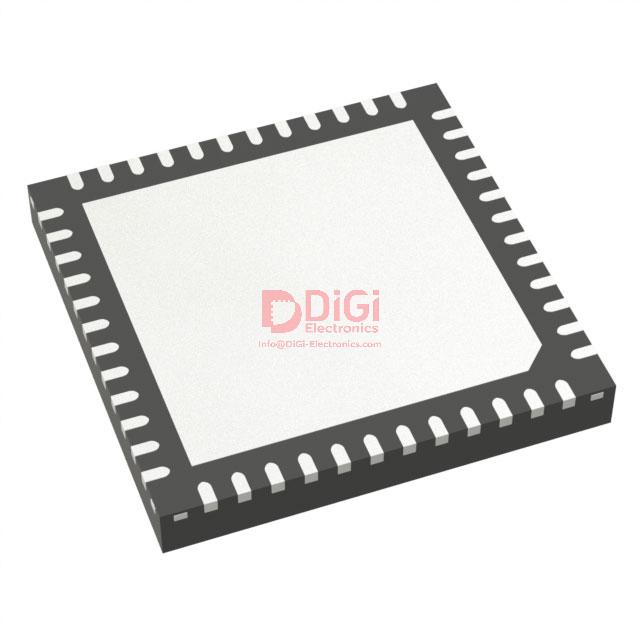
Electrical, mechanical, and package data for STM32H503CBU6
The STM32H503CBU6 is engineered for dense system integration, encapsulated in a 7x7 mm UFQFPN48 package that balances board area constraints with robust I/O accessibility. Focusing on harsh-environment suitability, its electrical and mechanical frameworks are optimized for operation across a wide temperature range: ambient support spans -40°C to +105°C, extendable to +125°C under reduced power thresholds, and a maximum junction rating of +130°C. This thermal capability is pivotal in industrial or automotive deployments, where exposure to extended temperature fluctuations is routine.
Compliance with RoHS3 and REACH directives, coupled with ECOPACK2 packaging, addresses contemporary requirements for environmental stewardship and long-term component sustainability. These ecological commitments extend usage relevance for green-certified designs and ensure supply chain compatibility for export-sensitive sectors.
Clock architecture within the STM32H503CBU6 is characterized by both redundancy and granularity. The MCU offers dual internal oscillators (64 MHz and 48 MHz), promoting autonomous core and time-critical subsystem operation while removing reliance on external timing components in cost- or power-sensitive configurations. For use cases that demand superior timing precision—such as wireless stacks or real-time control—external oscillators (HSE: 4–50 MHz; LSE: 32.768 kHz) are seamlessly integrated. The presence of two on-chip PLLs enables peripheral domains to be clocked independently; designers can assign clock trees to optimize for endpoint requirements—balancing throughput, power, and noise adaptation on a per-peripheral basis. In practice, careful PLL tuning can enable stable USB communications while locking system timers to precision low-speed crystals, improving temporal determinism across subsystems.
From a supply architecture perspective, the system mandates rigorous decoupling strategy at every power, I/O, and backup rail to contain noise and preserve signal integrity. The package’s thermal resistance (θJA/θJC) mandates deliberate PCB design, especially in applications with elevated ambient or pronounced dissipation. Following the manufacturer’s suggested copper pour and thermal pad recommendations is critical for maintaining operational bounds under heavy load. Evaluations have shown that placing multiple ground vias beneath the exposed pad and orienting thermal reliefs perpendicular to heat-flow gradients can reduce the risk of localized hotspots.
In summary, the STM32H503CBU6 serves as a flexible, eco-conscious MCU platform where detailed attention to clock planning, power decoupling, and package thermal management converges to enable durable operation across a multitude of tightly constrained form factors. Careful leveraging of its electrical and package features, guided by empirical layout best practices, unlocks its full operational envelope and longevity—particularly relevant in edge-device and high-temperature modular embedded applications.
Potential equivalent/replacement models for STM32H503CBU6
When evaluating equivalent or replacement options for the STM32H503CBU6, a methodical approach grounded in system requirements and future scalability is preferred. The STM32H503xx subfamily provides immediate alternatives with a range of package and pin-count variants—WLCSP25, UFQFPN32, LQFP48, and LQFP64. This granularity enables precise alignment to mechanical constraints and I/O needs, reducing PCB redesign and preserving signal integrity. Direct substitution within the H503xx ensures minimal firmware revision, aided by consistent peripheral layouts and register maps.
For designs encountering resource bottlenecks—such as data-intensive algorithms or extensive buffer usage—migrating to higher-memory STM32H5 variants leverages increased flash and SRAM, often with enhanced memory interfaces. This supports deep buffering or large lookup tables without the workarounds required by smaller MCUs. However, enlarging the memory footprint may introduce subtle differences in access speed or peripheral latency, necessitating timing validation during system bring-up.
When ultra-low power consumption or security features become focal, the STM32L5 series stands out. Its TrustZone and optimized sleep modes, together with fine-grained clock gating, enable secure, long-life applications typically found in wearables or battery-powered edge nodes. Conversely, should the application demand advanced analog front-ends, higher throughput, or rich graphics, the STM32H7’s dual-core architecture and improved peripherals accelerate development of high-performance, real-time solutions such as process controllers or industrial HMIs. Here, pin compatibility diverges; careful PCB and middleware analysis is required to avoid costly redesign cycles and ensure robust code porting. Peripheral-to-peripheral mapping breakdowns occasionally surface, primarily when leveraging H7-exclusive modules. Early prototype phase testing tends to uncover such gaps before volume commitment.
Specialized feature dependencies warrant heightened scrutiny. Applications integrating interfaces like I3C or employing dual-bank flash for robust firmware upgrades rely on the extended STM32H5 family, as baseline variants may lack these advanced blocks. For such projects, mapping peripheral features and validating register compatibility in the candidate MCUs averts deployment delays. Experience suggests that mixed-signal integrity and edge-case interrupt latencies deserve special attention in these migration scenarios.
Ultimately, the viability of each alternative hinges on transparent evaluation of electrical ratings, peripheral pinouts, and firmware revalidation effort. Unexpected firmware behaviors commonly arise from subtle differences in reset states, clock trees, or analog performance—even within the same general series. Rigorous reference to errata and rapid prototyping with candidate MCUs streamlines the path from bench to production while safeguarding long-term maintainability.
In practice, a layered comparative matrix—mapping core features, package compatibility, memory configuration, and specialized peripherals—proves decisive in narrowing candidate MCUs. Factoring in availability and lifecycle commitment adds resilience to supply chain disruptions, an increasingly pressing concern in recent design cycles. This technical diligence not only accelerates successful migration but also builds in architectural flexibility for future product iterations.
Conclusion
The STM32H503CBU6 exemplifies the convergence of high-performance processing and thorough analog-digital integration within a compact form factor. Built upon the STM32H5 architecture, this microcontroller leverages a Cortex-M33 core, optimized for both deterministic real-time execution and rapid interrupt response, which is essential in closed-loop control and mission-critical embedded systems. The embedded memory hierarchy—encompassing high-speed SRAM and Flash—facilitates complex algorithms, edge analytics, and custom protocol stacks without external dependencies, reducing latency and maximizing throughput.
Analog front-end functionality is seamlessly interwoven, including high-precision ADCs and configurable timers, supporting diverse sensor interfacing and signal acquisition demands. This enables precision monitoring, adaptive control, and low-noise measurements within industrial automation, medical instrumentation, and advanced robotics. Flexible digital I/O, fast GPIOs, and integrated communication peripherals further streamline hardware design, lowering the integration barrier for sophisticated connectivity topologies and modular expansion.
Security architecture is implemented at the silicon level, aligned with requirements for device identity, firmware protection, and secure boot. Hardware cryptographic accelerators and unique device secret provisioning support trusted execution environments, laying the foundation for secure over-the-air firmware updates and secure communication protocols. This approach mitigates risks associated with compromise vectors that software-only defenses struggle to address over the lifecycle of an IoT or industrial deployment.
From a pragmatic development perspective, the STM32H503CBU6 supports scalable product platforms through compatibility with established STM32 ecosystems—development tools, middleware stacks, and reference designs. This ecosystem accelerates time-to-market while allowing tight control over customization and optimization cycles. The device's multipronged support for connectivity, including SPI, UART, and advanced peripherals like CAN FD, anticipates evolving industrial protocols and ensures seamless migration to next-generation networks without redesign overhead.
The selection process for this microcontroller should be driven by an understanding of both immediate application requirements and projected security/compliance trajectories. The inherent flexibility of the STM32H503CBU6 allows implementers to address not only present computational and I/O needs but also futureproof platforms against emerging attack surfaces and interoperability standards. In practice, its robustness in field environments, combined with upgradable security features and hardware-backed reliability, frequently turns the device into a strategic enabler for long-term industrial and connected deployments. This synthesis of performance, integration, and security is increasingly recognized as indispensable for sustainable embedded solutions.


