>
>


Product overview: STM32F427VIT6TR from STMicroelectronics
At the fundamental level, the STM32F427VIT6TR integrates an ARM Cortex-M4 core equipped with a hardware Floating Point Unit, which is instrumental for real-time signal processing and computation-intensive control loops. Operating at 180 MHz, this microcontroller executes up to 225 DMIPS, positioning itself favorably for latency-sensitive applications requiring deterministic performance and high efficiency. The core architecture leverages pipeline optimization and advanced instruction sets, fluently balancing throughput and energy consumption—a critical consideration in industrial control scenarios where prolonged uptime and thermal management are non-negotiable.
Peripheral integration on the STM32F427VIT6TR is engineered to maximize system modularity and reduce external component count. Alongside standard interfaces such as UART, SPI, I2C, and CAN, the microcontroller offers multiple timers, PWM generators, ADCs with high conversion speeds, and rich connectivity options including USB OTG FS/HS and Ethernet (MAC layer). These embedded peripherals facilitate robust signal acquisition, motor control, and wired/wireless communication frameworks. By streamlining GPIO mapping over the 100-LQFP form factor and providing flexible alternate functions, the device greatly accelerates prototyping cycles and lowers PCB complexity.
The STM32F427VIT6TR incorporates sizable memory blocks, including up to 2 MB of Flash and 256 KB of SRAM, supporting sophisticated firmware structures and multi-threaded RTOS environments. Such an architecture empowers developers to deploy embedded AI inference, intricate data logging, or secure boot features. The memory controller also enables seamless interfacing with external memory devices, extending capacity for real-time data buffers or graphical workloads. Experience in deploying this device underlines the necessity of precise memory partitioning for optimal task concurrency and minimizing interrupt latency.
Power management is vital for deployment in electrically constrained environments. The microcontroller supports dynamic voltage scaling, multiple sleep modes, and integrated brownout reset, ensuring resilience against supply-side instabilities while maintaining rapid wake-up times. This requires methodical calibration of system clocks and power domains, particularly within industrial automation or IoT edge nodes where predictable recovery and low standby current dictate application viability.
Application scenarios encompass advanced motor drive systems, industrial sensor networks, and secure gateways for industrial IoT infrastructures. In high-speed data aggregation or edge analytics, the FPU accelerates matrix calculations, FFTs, and Kalman filtering, condensing processing latency and enabling sophisticated control algorithms. The intrinsic reliability of this device in electromagnetic-noisy environments has been validated through real-world deployments—firmware engineers favor its fault-tolerant peripherals and deterministic interrupt management for mission-critical use-cases.
A unique insight emerges from the synergy between hardware and software scalability encoded within the STM32F4 ecosystem. Firmware migration paths and middleware compatibility are supported across the series, providing a resilient foundation for platform-centric product lines. The STM32F427VIT6TR, thus, not only addresses immediate engineering challenges but also ensures future-proofing through pin-to-pin compatible upgrades and consistent toolchain integration, underscoring its strategic advantage in advanced embedded design.
Core architecture and performance features of STM32F427VIT6TR
The STM32F427VIT6TR integrates an ARM 32-bit Cortex-M4 processor core, specifically designed to address the compute and response demands of modern embedded systems. Central to its architecture is a patented Adaptive Real-Time (ART) accelerator, which facilitates zero wait-state access to embedded Flash memory at the maximum supported clock frequencies. This mechanism leverages prefetching and instruction pipeline optimization, ensuring that the processor core maintains a continuous data flow even during intensive instruction fetch cycles. By reducing execution stalls often encountered in high-frequency operation, the ART accelerator eliminates the throughput limitations traditionally imposed by embedded Flash, thus enabling sustained real-time execution without CPU starvation.
Beyond its core pipeline, the Cortex-M4 features a comprehensive set of single-cycle multiply-accumulate and SIMD DSP instructions. This capability elevates the microcontroller’s suitability for signal processing workloads such as motor control, digital filtering, or sensor fusion. Deterministic interrupt latency, guaranteed by a tightly-coupled nested vectored interrupt controller (NVIC) and the predictable memory subsystem, proves advantageous in closed-loop control designs and time-sensitive acquisition systems, where jitter and unpredictable delays cannot be tolerated. The optional Memory Protection Unit, efficiently partitioning memory regions, enforces robust isolation between critical firmware segments, helping mitigate inadvertent cross-section data corruption or code execution faults. This layer is particularly valuable in SIL or IEC 61508 safety certification environments, where memory isolation is a non-negotiable requirement.
System designers also benefit from high-bandwidth communication interfaces—including multiple SPI, I2C,USART, and CAN peripherals—supported by dedicated DMA controllers. This data path offloading empowers the MCU to handle real-time protocol implementation or high-volume sensor polling with minimal intervention from the central processor. In practice, the STM32F427VIT6TR consistently meets deterministic timing constraints in data-intensive acquisition setups, such as those found in industrial automation, signal instrumentation, and advanced motor control platforms. An important observation is the synergy between the DSP core and the ART accelerator: compute-bound DSP loops in tightly controlled acquisition cycles can run at full core speed, unhampered by memory wait states, translating directly to predictably high sampling rates and control bandwidth.
Applications deploying the STM32F427VIT6TR realize tangible benefits in overall system responsiveness and stability, particularly where deterministic execution directly impacts system-level outcomes. Leveraging the flexible Flash architecture and memory protection features, firmware updates and modular code architectures can be deployed with reduced integration risk. Such modularity, coupled with the real-time performance envelope, enables scalable design strategies—from single-board prototypes to functionally safe industrial nodes—without sacrificing core timing or bandwidth requirements. This layered integration of CPU, memory subsystem, and isolation primitives reflects a nuanced understanding of the challenges faced in embedded systems, notably the persistent trade-off between throughput and reliability. The STM32F427VIT6TR stands out by shifting this trade-off boundary, accommodating both aggressive real-time targets and rigorous safety constraints within a unified platform.
On-chip memory, memory architecture, and expansion capabilities of STM32F427VIT6TR
The STM32F427VIT6TR integrates a robust memory subsystem tailored for demanding embedded applications. The dual-bank 2 MB Flash architecture enables concurrent program execution and background firmware updates through read-while-write, minimizing system downtime during code deployment. This is particularly beneficial in operational scenarios requiring non-interrupted service, such as real-time industrial control or rapid firmware iteration. The Flash's sector organization and integrated ECC further enhance data integrity, allowing developers to implement reliable code shadowing, field upgrades, and secure partitions for critical routines.
SRAM resources are comprised of a 192 KB main block, 64 KB core-coupled cache (CCRAM), and a dedicated 4 KB backup SRAM powered via VBAT. The combination yields improved parallelism for high-throughput tasks, ensuring large buffers for graphics processing or protocol stacks can coexist with real-time application data. The architecture supports low-latency buffer management, making amortized context switching feasible in multitasking RTOS deployments. Backup SRAM provides persistent storage for runtime state, facilitating rapid system recovery in power loss scenarios without external retention circuits.
The inclusion of 512 bytes of One-Time Programmable (OTP) memory aligns with secure provisioning requirements. This non-volatile area is suitable for unique device identifiers, cryptographic keys, or tamper-evident flags that must remain immutable throughout the product lifecycle. OTP integration strengthens secure boot implementations and key management schemes by isolating critical secrets from standard firmware areas.
Extensive external memory support is achieved through the Flexible Memory Controller (FMC), which accommodates asynchronous and synchronous peripherals over a 32-bit parallel interface. Developers can choose from SRAM, PSRAM, SDRAM or LPSDR SDRAM, and NOR/NAND Flash, leveraging either volatile workspace expansion or persistent storage for massive datasets. The FMC design includes adjustable timings, bank mapping, and error filtering, streamlining the attachment of external memory chips while maintaining deterministic access patterns. This flexibility is instrumental in implementing large display framebuffers, high-frequency logging modules, or in-memory databases characteristic of edge computing and automation platforms.
There is significant value in balancing on-chip/external memory utilization. For time-critical firmware sections and frequently accessed RTOS objects, on-chip SRAM, benefiting from low access latency, is preferred. Peripheral data streaming and large, non-time-sensitive data sets, such as historical logs or media buffers, are offloaded to expandable FMC-attached memories. System designers often fine-tune data placement after benchmarking representative workloads, gaining measurable improvements in task response times and non-blocking I/O performance.
Strategic leveraging of the STM32F427VIT6TR’s layered memory architecture supports advanced multi-threaded capability, robust data retention across resets, and scalable integration of storage-intensive modules. Practical deployment experience indicates that thoughtful separation of firmware overlays and persistent data zones significantly boosts reliability and simplifies field maintenance processes. By embedding security primitives into OTP and optimizing SRAM allocation, system resilience and security posture are improved without sacrificing application throughput. Thus, the STM32F427VIT6TR exemplifies a high-density memory design, facilitating the transition from single-purpose controllers to sophisticated, feature-rich nodes in complex distributed systems.
Integrated peripherals and connectivity options in STM32F427VIT6TR
The STM32F427VIT6TR microcontroller exemplifies contemporary design by integrating an expansive range of peripherals, thereby optimizing system architecture for performance, flexibility, and resource efficiency. At the foundational level, the inclusion of multiple communication interfaces anticipates demanding use cases and heterogeneous system requirements. Three dedicated I2C controllers enable robust connectivity with an array of sensors and low-speed peripherals, facilitating sensor fusion, real-time monitoring, and smart actuation—key requirements in precision measurement and industrial automation scenarios where I2C multiplexing and address space play critical roles.
Six SPI modules, with two supporting full-duplex I2S, provide both high-throughput serial connectivity and versatile audio data transfer capabilities. This modularity is essential in applications requiring simultaneous communication with multiple SPI devices, such as high-speed ADCs, DACs, and memory chips, streamlining concurrent data acquisition and storage. The full-duplex I2S operation further expands the device’s suitability for complex digital audio systems, supporting real-time audio streaming with tight timing constraints. Circuit board designs can isolate SPI domains, optimizing EMC performance by selectively routing critical signals while leveraging the microcontroller’s flexible pin mapping.
The provision of four USART/UART interfaces, each capable of asynchronous communication, enables straightforward integration with legacy RS-232/RS-485 networks and allows simultaneous serial links—an advantage in distributed control environments, modular device stacks, and systems requiring extensive diagnostic communication. With two independent CAN 2.0B controllers, the device serves real-time, safety-critical applications including automotive ECUs and industrial CANopen nodes. CAN hardware filtering, message buffer flexibility, and robust error management enhance network reliability and deterministic message delivery in harsh environments.
Ethernet connectivity, realized via an integrated MAC supporting IEEE 1588v2 Precision Time Protocol and DMA, delivers deterministic packet processing, enabling the microcontroller to act as both a time-aware node and a gateway in distributed motion control and synchronization networks. The dedicated DMA engine decouples data movement from CPU intervention, sustaining line-rate throughput for protocols like EtherCAT or industrial TCP/IP stacks. The design consideration of integrating MAC with PTP support signals readiness for convergent operational technology networks where latency and network determinism define system-level KPIs.
Incorporation of SDIO and USB OTG (with integrated PHY) introduces further interoperability with mass storage and portable devices. High-speed/full-speed USB OTG, encompassing both host and device modes, streamlines firmware updates, human-machine-interfacing, and persistent mass storage expansion without discrete USB controllers, while direct support for SDIO accelerates implementation of SD cards and legacy multimedia peripherals. Practical project experience shows that leveraging on-chip PHYs reduces board space and shielding requirements, easing the transition from concept to manufacturable hardware.
A central insight emerges: such comprehensive peripheral integration is not solely about maximizing feature sets, but about strategically aligning the microcontroller with evolving system architectures where mixed-protocol environments proliferate. The STM32F427VIT6TR’s layout reduces external logic demand and minimizes the bill of materials, directly impacting bottom-line costs and enabling more aggressive PCB real estate management—this is particularly consequential in cost-sensitive, high-density applications such as industrial controllers, IoT edge devices, and embedded vision platforms.
This orchestration of diverse integrated connectivity, combined with flexible DMA engines and protocol-specific hardware acceleration, positions the device as a convergence layer between legacy fieldbuses and high-performance, networked automation. Designs built around this platform consistently realize reduced validation cycles, consistent signal integrity, and simplified regulatory compliance due to reduced external interconnections—all outcomes rooted in the engineering-centric integration philosophy intrinsic to the STM32F427VIT6TR.
Analog, timer, and clock resources in STM32F427VIT6TR
The STM32F427VIT6TR implements a robust analog subsystem with three independent 12-bit ADCs. Each ADC features a conversion rate up to 2.4 MSPS, enabling rapid acquisition of fast-changing analog signals in multi-channel monitoring environments. Through hardware-supported triple interleaving, the system reaches an aggregate throughput of 7.2 MSPS, which is critical for tasks like simultaneous multi-phase current sensing in high-speed motor drives or high-fidelity data acquisition for industrial sensors. Fine control of sampling utilizes programmable sample times and sequencer logic, optimizing analog front-end design for varied impedance sources.
Complementing the acquisition side, the two integrated 12-bit DACs provide deterministic analog output for closed-loop process control, waveform generation, and system self-testing routines. The DACs interface seamlessly with DMA controllers, supporting jitter-free streaming of digital-to-analog conversion in real-time feedback loops or precision signal synthesis applications.
Timing resources in the microcontroller are notable for their granularity and versatility. There are twelve 16-bit general-purpose timers, two 32-bit timers for extended duration operations, and two advanced control timers configured for synchronized PWM generation. Encoder mode integration allows direct decoding of incremental position feedback signals without external logic, which significantly simplifies hardware for robotics and industrial drive systems. Input capture and output compare capabilities enable accurate timestamping and event scheduling, instrumental in closed-loop digital control and synchronized multi-axis actuation.
The real-time clock subsystem centers on a hardware-accelerated calendar with subsecond resolution. This RTC is backed by a dedicated VBAT domain, eliminating dependency on primary power rails and maintaining temporal continuity through power events—a crucial consideration for critical process logging, fault event diagnostics, and time-sensitive automation controls. Multiple oscillator sources underpin this timing architecture. The device accepts external crystals in the 4–26 MHz range for low-jitter timing and system clocking, while the internal 16 MHz RC oscillator serves as a rapid startup or fallback source. The dedicated 32 kHz crystal oscillator drives the RTC independently, allowing for ultra-low-power deep sleep states while retaining precise timekeeping.
System-level integration of these resources enables highly adaptable application engineering. In multi-axis motor control scenarios, advanced control timers synchronize PWM outputs with feedback from ADC-based current sensors and position-encoded shaft information, facilitating robust field-oriented control algorithms. In industrial throughput monitoring, rapid ADC sampling combined with accurate timestamping supports continuous, high-resolution trend analysis. Flexible clocking options ensure all subsystems maintain optimal timing coherence, lowering susceptibility to EMI and drift while supporting power management strategies through selective clock domain activation.
Experience shows that prioritizing timer allocation and clock source assignment early in system architecture dramatically reduces debugging cycles and reliability issues downstream. Implementing DMA-driven ADC and DAC workflows minimizes CPU load while maximizing deterministic timing, key for real-time control systems. Utilizing the device's interleaved ADC mode, paired with concurrent use of output compare channels, consistently results in superior throughput for multi-channel measurements.
The STM32F427VIT6TR’s resource set is engineered for exacting applications. Its layered peripheral design, from low-level sampling to high-level coordinated control, enables scalable solutions across demanding fields—ensuring the device achieves optimal trade-offs between performance, flexibility, and power consumption. The implicit synergy between analog, timing, and clock domains within the hardware forms the foundation for designs that require precise, responsive interactions in challenging automation and control environments.
Power supply, operating conditions, and package details for STM32F427VIT6TR
The STM32F427VIT6TR microcontroller demonstrates considerable flexibility in power architecture, accommodating a supply voltage range between 1.8 V and 3.6 V for core operation and 1.7 V to 3.6 V for its I/O domain. This adaptability ensures compatibility with diverse external circuitry and power rails, facilitating seamless integration into systems where supply variation might arise due to battery discharge profiles or fluctuating industrial power sources. Internal mechanisms such as Power-On Reset (POR), Brown-Out Reset (BOR), and Programmable Voltage Detector (PVD) are tightly woven into the supervisory fabric, offering deterministic startup and rapid recovery from undervoltage events. These features mitigate erratic system behavior, maintaining data integrity and operational predictability amidst dynamic power conditions.
Extended industrial temperature tolerance from −40°C to +85°C empowers deployment across a spectrum of application settings, from climate-controlled enclosures to environments characterized by thermal shocks and sustained extremes. This broad range is notably significant when targeting automation, transportation, or outdoor instrumentation, where thermal reliability must match stringent operational requirements. Real deployments have underscored the necessity of meticulous PCB design—especially thermal dissipation strategies and package placement—to fully leverage specified limits over extended lifecycles.
Ultra-low-power operational modes, including Sleep, Stop, and Standby, are engineered for rapid context switching and minimal leakage, affording granular control over energy consumption. Fast wakeup capabilities are paramount for systems executing periodic sensor sampling, wireless event detection, or user-triggered actions. During integration, selecting appropriate mode transitions and fine-tuning clock domains are critical for balancing latency, responsiveness, and power draw. Empirically, fine-grained mode management yields measurable improvements in battery longevity and minimizes the need for oversized energy reserves, especially in edge devices.
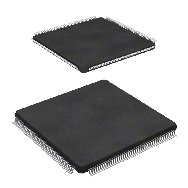
In terms of physical implementation, the 100-lead LQFP package achieves high I/O density within a manageable footprint, addressing the spatial constraints often dictated by modern embedded platforms. Up to 82 assignable I/O pins allow significant interface expansion, while broader STM32 family variants scale pin count and voltage tolerance to facilitate higher throughput or specialized signal compatibility. Experienced engineers often exploit flexible pin multiplexing and advanced PCB signal routing to maximize functional integration without incurring signal integrity or crosstalk penalties. Judicious use of the 5 V-tolerant fast I/O lines is essential where legacy peripherals must be supported alongside new high-speed interfaces.
A cohesive design approach to the STM32F427VIT6TR leverages its versatile electrical, mechanical, and power management capabilities to address emerging requirements in industrial automation, remote sensing, and advanced human-machine interfaces. The capacity to combine robust environmental tolerance with finely tuned energy profiles enables high-reliability system performance, while the compact package and expanded I/O configuration sustain scalability in densely populated electronic assemblies. This convergence of features, when judiciously integrated during board-level design and system validation, frequently results in enhanced system stability, longer operational uptime, and lower total cost of ownership.
Security, reliability, and development support in STM32F427VIT6TR
Security and reliability in the STM32F427VIT6TR stem from a layered hardware and firmware architecture designed for demanding environments where robust protection and consistent operation are critical. At the foundation, hardware-accelerated CRC modules enable rapid integrity checks across memory blocks and communication payloads, minimizing processor overhead while ensuring real-time error detection. This mechanism is coupled with the true random number generator, a key asset for cryptographic protocols; it generates non-deterministic values suitable for session keys, device authentication, and transport-level security. The embedded 96-bit unique device ID underpins secure provisioning and traceability, forming a tamper-resistant anchor for secure boot, asset registration, and trusted firmware updates.
The platform’s reliability is fortified further by dual-system watchdogs—an independent watchdog functioning autonomously and a windowed watchdog with programmable timing. These components vigilantly monitor firmware execution and recall system stability in event-driven scenarios, such as memory leaks or peripheral malfunctions. Layered on-chip diagnostics, including a high-precision temperature sensor for silicon health monitoring, mitigate thermal drift and prolong device life in control systems exposed to fluctuating industrial conditions. Integrated SWD/JTAG debug interfaces and hardware trace resources create an environment conducive to rapid code validation and performance profiling, dramatically shortening iterative development cycles and enabling post-deployment fault analysis.
Operational experience demonstrates that leveraging hardware CRC at both communication endpoints and memory regions substantially reduces undetected bit errors in high-noise environments—a frequent occurrence in factory automation and remote sensing applications. Employing the TRNG supports cryptographically secure device pairing in wireless sensor networks, preventing replay attacks and unauthorized access. The combination of watchdog timers and silicon health sensors forms a resilient self-healing logic, allowing safety-critical systems to autonomously recover from transient faults without manual intervention—a vital feature in unattended installations.
Compliance with RoHS3 and REACH “unaffected” standards extends device longevity and regulatory reach, eliminating the need for late-stage redesigns due to material restrictions while supporting sustainable deployment cycles. The adoption of ECOPACK2 packaging not only streamlines SMT manufacturing by accommodating advanced soldering profiles, but also integrates seamlessly with automated optical inspection processes, reducing yield loss and improving scalability.
The underlying approach exemplifies a holistic integration of security primitives and reliability controls, tailored for modern industrial use cases where downtime and data breaches are unacceptable. These capabilities position the STM32F427VIT6TR as a core element in secure edge devices, safeguarding assets and ensuring dependable operation in evolving industrial and IoT landscapes.
Potential equivalent/replacement models for STM32F427VIT6TR
When evaluating potential alternatives or replacements for the STM32F427VIT6TR, it is essential to dissect the microcontroller’s functional core and map it to adjacent series within the STM32 ecosystem. The STM32F427xx and STM32F429xx lines share a common ARM Cortex-M4 architecture, ensuring seamless code portability and peripheral compatibility across different pin and memory configurations. Models like STM32F427II and STM32F427AI retain architectural uniformity but offer deviations in flash size and package format, catering to applications that prioritize PCB footprint or cost optimization while maintaining critical performance thresholds.
Moving upward within the family, larger variants such as STM32F429VI and STM32F429ZI differentiate themselves not only through expanded I/O count and memory resources, but more importantly by integrating an LCD-TFT controller and Chrom-ART hardware acceleration. The latter provides substantial throughput improvement in UI-rich systems, where framebuffer transfers and real-time alpha-blended graphics dominate system workload. Migration to these variants benefits designs experiencing upward scaling or branching into HMI-driven product ranges, without sacrificing software investment or underlying real-time determinism.
A nuanced decision framework emerges when balancing pin compatibility with feature deltas. For example, the absence of dedicated graphical acceleration in the STM32F427VIT6TR may restrict its operational envelope in display-centric deployments, whereas analogous STM32F429 models can unlock richer user interfaces with minimal board-level adaptations. At the silicon layer, all these devices leverage tightly coupled memories, advanced DMA engines, and flexible clocking options—which streamline the transition process and reduce time-to-market during component substitutions, especially under constraints dictated by supply chain disruptions.
Real-world migration experience demonstrates the tangible advantage of maintaining a unified STM32 platform in medium and high-volume embedded product lines. Board layout adjustments are often minimal due to consistent pin mapping across LQFP, BGA, and WLCSP packages. Firmware reuse is typically above 90%, with peripheral abstraction simplifying retargeting at the HAL or CMSIS-Driver level. When shifting from the STM32F427 to the STM32F429 series, targeted validation of display, graphical, and memory interfaces ensures risk mitigation while unlocking differentiated market positioning.
A layered approach to selection minimizes engineering friction: starting at the architectural baseline, evaluating peripheral spread and integrated IP blocks, and then optimizing at the board package and application tier. This incremental process not only accelerates hardware iterations but also supports long-term maintenance and future feature expansion with minimal sunk costs. Flexibility at the platform level directly translates to resilience in the face of component obsolescence, design pivots, or the introduction of new requirements within a maturing product roadmap.
Conclusion
The STM32F427VIT6TR, belonging to STMicroelectronics' flagship STM32F4 family, exemplifies an optimal intersection of processing power, peripheral depth, and configurability essential for advanced embedded systems. Centered around an ARM Cortex-M4 core with FPU, its computational throughput is well-suited for demanding control loops, signal processing, and real-time tasks seen in precision automation, industrial gateways, and networked measurement platforms. The 180 MHz clock, supported by up to 2 MB of on-chip Flash and 256 KB RAM, delivers not only raw performance but also the architecture needed for multithreaded firmware, secure boot management, and firmware-over-the-air updates in connectivity-centric deployments.
Peripheral richness is evident in its suite of high-bandwidth interfaces: dual CAN, multiple SPI/I2C/UARTs, and an integrated Ethernet MAC with advanced DMA. Such diversity accelerates design cycles for systems needing seamless fieldbus integration, chained sensor arrays, or deterministic communication in Industry 4.0 and IIoT architectures. The inclusion of advanced timers—many with PWM and input capture—streamlines motion control and electrophysical actuation, reducing the reliance on external logic and enhancing response determinism. Additionally, the presence of high-resolution ADCs/DACs enables direct interface to analog plant variables, vital in closed-loop systems typical in robotics or smart instrumentation.
From a hardware reuse standpoint, the pinout consistency across the STM32F4 portfolio, combined with flexible clock and power domains, supports scalable platform designs. Board-level transition from proof-of-concept to production becomes less burdensome, especially when leveraging ST’s mature HAL/LL libraries and equipping projects with FreeRTOS or CMSIS-RTOS. Practical implementation highlights the device's robust EMI/EMC tolerance and stable operation under fluctuating industrial power conditions, attributes often validated through repetitive exposure to harsh on-site environments and aggressive stress testing.
Strategically, incorporating the STM32F427VIT6TR in product roadmaps not only secures long-term supply confidence but also capitalizes on cross-compatibility with a widely supported ecosystem—toolchains, middleware stacks, and community-validated reference designs. This paves the way for smoother compliance pathways (IEC 61508, UL/CE, etc.) and minimized learning curves when onboarding new development resources or evolving existing designs.
Analyzing deployment data reveals that optimal results stem from early architectural alignment: partitioning tasks to exploit the core's DSP, leveraging built-in hardware cryptography for secure edge applications, and architecting firmware with modularity for over-the-air maintenance. The STM32F427VIT6TR, when utilized with this integrative engineering approach, not only extends system lifetime but also anchors a sustainable legacy of scalable, reliable, and high-performance embedded solutions.