 >
>


Product overview of STM32F373CBT7 STMicroelectronics microcontroller
Engineered around a 32-bit ARM Cortex-M4 core, the STM32F373CBT7 microcontroller delivers a notable blend of computational performance, precision, and peripheral integration at a power envelope tailored for embedded designs. Operating at frequencies up to 72 MHz, the device natively supports hardware floating-point operations through its integrated FPU, accelerating signal processing tasks and real-time control algorithms while minimizing software overhead. This architectural decision eliminates bottlenecks commonly observed when emulating floating-point math on integer-only cores, especially relevant for applications reliant on digital filtering, control loops, or sensor fusion.
The internal memory architecture comprises 128 KB Flash and 32 KB SRAM, balancing code density with efficient data handling. Code execution from on-chip Flash is tightly optimized owing to the advanced bus matrix and prefetch logic, sustaining deterministic latency for control-critical routines. SRAM capacity supports demanding buffering scenarios, such as concurrent data acquisition or multi-protocol stack management.
The microcontroller’s mixed-signal prowess is embodied in its array of analog peripherals. Precision 16-bit sigma-delta ADCs, high-resolution DACs, and integrated comparators enable direct interfacing with a wide spectrum of sensors and actuators. This facilitates designs requiring analog front-end conditioning, high-fidelity measurables, or electrical parameter monitoring. Experienced practitioners exploit integrated PGA and calibration circuits to mitigate offset and drift effects, reducing BOM complexity and enhancing long-term measurement stability. The availability of multiple ADC channels and flexible trigger logic streamlines real-time acquisition from multiple input sources, a frequent requirement in industrial automation or medical instrumentation.
Digital peripherals reinforce versatility in connectivity and control. Standard communication interfaces such as USART, SPI, I2C as well as advanced timers empower tasks from protocol handling to fine-grained pulse-width modulation and event synchronization. Engineers often leverage the hardware PWM features or input capture for motor control applications, taking advantage of hardware-based dead-time insertion and frequency resolution that support precise actuator feedback and closed-loop regulation.
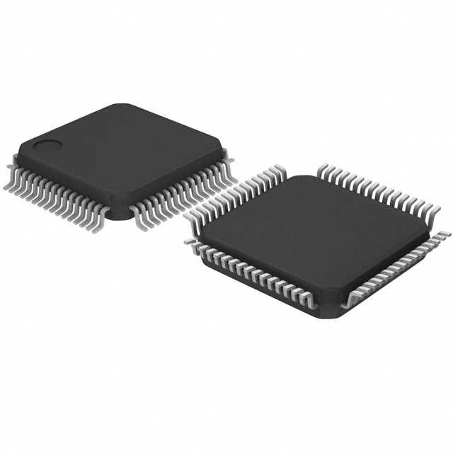
With its pin-efficient 48-pin LQFP package, the STM32F373CBT7 provides a compact footprint amenable to space-limited boards. Designers executing efficient floorplanning can route high-frequency signal traces and sensitive analog nodes with minimal crosstalk, while achieving robust EMC behavior required by industrial and medical standards.
The core insight underpinning successful deployment of the STM32F373CBT7 resides in judicious peripheral selection and resource mapping, maximizing parallel processing across analog and digital domains. This approach unlocks the microcontroller’s capability to host multi-modal sensing and control systems with reduced latency and enhanced signal integrity. In practice, implementations often intertwine DMA-driven data streams and interrupt prioritization, ensuring high-throughput performance without sacrificing deterministic response—a constant priority in mission-critical embedded platforms. Engineers optimizing for these strengths realize not only functional integration but also accelerated development cycles due to the microcontroller’s tooling ecosystem and extensive library support.
Architecture and core features of STM32F373CBT7 STMicroelectronics
The STM32F373CBT7 microcontroller, manufactured by STMicroelectronics, is anchored by the ARM Cortex-M4 processor core, engineered for real-time embedded control applications requiring both computational throughput and deterministic behavior. The Cortex-M4’s pipeline architecture enables single-cycle execution of multiply and divide instructions, which accelerates operations central to control algorithms often encountered in motor control or digital signal processing. The comprehensive DSP instruction set, combined with integrated hardware floating-point capability (via the optional FPU), permits in-situ execution of fixed- and floating-point arithmetic without external coprocessor overhead, streamlining both throughput and power consumption in signal-path implementations such as sensor filtering, audio processing, or control loop compensation.
To safeguard critical memory regions, the microcontroller incorporates a hardware MPU, enforcing privilege separation and mitigating the risk of errant or malicious code compromising key resources or control structures. This mechanism is instrumental in RTOS-based deployments, where multiple tasks with varying trust levels coexist, enabling fine-grained control over memory access policies and reducing system-level vulnerabilities.
The debugging infrastructure is further reinforced by the Embedded Trace Macrocell (ETM), facilitating non-intrusive, cycle-accurate tracing of program execution. This proves invaluable when diagnosing subtle timing-dependent issues in interrupt-driven systems, optimizing context switch strategies, or verifying the integrity of fault-handling routines. In practice, trace data gathered via ETM expedites root-cause analysis and enhances coverage of safety-critical code paths, aligning with industry requirements for functional safety certification.
Architectural optimization of the STM32F373CBT7 extends beyond core compute and debugging features. Its internal peripherals—timers, analog-to-digital converters, and communication interfaces—are designed for low-latency interaction with real-world signals, complemented by direct memory access (DMA) capabilities that reduce CPU overhead for high-bandwidth data transfers. Deployments in industrial automation routinely leverage these features for deterministic event response and closed-loop regulation, minimizing jitter and cycle time variance.
Considering practical integration, the alignment of hardware security (via MPU), rich signal processing resources (DSP, FPU), and advanced debugging (ETM) within a single device enables scalable migration from prototype to production. RTOS interoperability is streamlined, with application code able to exploit fine-grained memory protection and deterministic scheduling. In application scenarios such as field-oriented motor control, multi-channel sensor fusion, or real-time diagnostics, these architectural choices translate into enhanced resilience, performance, and maintainability under challenging field conditions.
The STM32F373CBT7’s layered engineering approach, bridging robust core architecture and peripheral efficiency, distinctly elevates its suitability for complex, time-sensitive control systems. The fusion of DSP capability and granular security with hands-on debugging unlocks avenues for innovation while maintaining operational confidence—even as deployed systems scale in complexity and safety requirements.
Embedded memory in STM32F373CBT7 STMicroelectronics
The STM32F373CBT7 integrates a balanced embedded memory architecture tailored to real-time application demands. Equipped with 128 KB of on-chip Flash, the device accommodates substantial application code and data storage, supporting both bootloader and main firmware coexistence. The 32 KB SRAM complements Flash by enabling buffer-intensive routines and concurrent data processing, with hardware-level parity checking bolstering error detection. This parity mechanism operates transparently, introducing negligible latency while significantly mitigating the risk of silent data corruption—a critical consideration in safety-oriented systems such as industrial control or instrumentation.
Flash memory access is highly optimized via a dynamic wait state controller, with zero wait state operation maintained for CPU frequencies up to 24 MHz. This design ensures deterministic fetch performance, essential for interrupt-driven systems and time-constrained control loops. At elevated clock speeds, incremental wait states are introduced automatically to preserve data integrity, preventing resource conflicts. In practice, tuning the system clock in harmony with Flash wait state configurations delivers consistent code execution without timing anomalies, which is vital during in-field upgrades or when deploying certified software modules.
A robust boot mode selector underpins several firmware deployment and recovery scenarios. At power-on or reset, the system can boot from user Flash, system memory (typically a factory-embedded bootloader), or SRAM. This tri-modal approach proves invaluable for implementing firmware update protocols, as applications can switch to system memory for secure re-flashing, or leverage SRAM boot to execute diagnostics or temporary routines. During field servicing or recovery from failed updates, the ability to re-map boot vectors minimizes downtime and streamlines restoration procedures.
The integrated CRC calculation unit is architected to offload data integrity verification from the CPU, allowing on-the-fly CRC computation of Flash-resident code or RAM-stored buffers. This hardware acceleration favors cyclic redundancy checks as part of functional safety routines, particularly in segments subject to regulatory compliance such as medical instrumentation and automotive sensor nodes. By invoking the CRC unit within an interrupt handler or a real-time task, system designers safeguard program memory and critical data structures with minimal overhead and deterministic timing—a pattern proven effective in robust embedded software engineering.
When optimizing the STM32F373CBT7 for reliability-centric projects, partitioning Flash for atomic updates and employing SRAM's parity capabilities for all high-priority buffers elevates system resilience. Furthermore, leveraging hardware CRC not only during boot but periodically during runtime enhances long-term operational integrity. The cumulative memory subsystem design presents a scalable foundation, supporting both rapid prototyping and deployment in environments with stringent dependability requirements.
Power management and low-power capabilities of STM32F373CBT7 STMicroelectronics
Power efficiency in embedded systems hinges on the sophistication of microcontroller power management mechanisms. The STM32F373CBT7 integrates a suite of finely tunable features around its supply voltage flexibility, providing a functional range between 2.0 V and 3.6 V that aligns with diverse battery chemistries and external power sources. System architects can adjust the supply voltage dynamically, trading off operating speed for lower consumption or boosting performance as required by workloads.
Granular voltage monitoring is enabled via configurable power-on and power-down detectors. These modules proactively safeguard against brown-out conditions and allow for intelligent system responses, such as early warning interrupts or controlled shutdown sequences. Power domains within the STM32F373CBT7 are partitioned to isolate critical blocks, exploiting programmable voltage detectors to optimize real-time reliability without sacrificing efficiency.
The embedded power management core offers multiple low-power operating states, each targeting specific use cases. Sleep mode halts CPU operation but keeps peripherals responsive to trigger events, providing microsecond-level wakeup latencies while maintaining system context. In Stop mode, deeper quiescence is achieved: the main clock halts, but SRAM and register contexts persist, supporting rapid restoration of operation after wakeup. Use of Stop mode is widespread in cyclically active sensor nodes, where data retention and swift duty cycling are mandatory.
Standby mode employs a rigorous shutdown: almost all internal regulation ceases, volatile memory is lost except for the RTC and backup registers which are sustained through a dedicated VBAT supply ranging from 1.65 V to 3.6 V. This mode is instrumental when targeting ultra-low quiescent currents for seasonal devices, or when state preservation is only necessary for minimal timekeeping or last-state information.
In practice, mode transition speeds and context preservation are crucial; leveraging the embedded wakeup logic, engineers reduce latency and synchronize real-time tasks precisely. For instance, implementing multi-tier interrupt-driven wakeups in Sleep or Stop mode enables flexible event handling without a substantial increase in current draw. In standalone environmental monitors, long intervals of inactivity can be bridged by Standby mode, with RTC-driven timers orchestrating periodic wakeups—resulting in tangible battery life extensions measured in months rather than weeks.
A nuanced consideration emerges in balancing power domains and peripheral enablement: selectively powering down unused interfaces or analog blocks upholds tight energy budgets. Employing a hierarchical sleep strategy—cycling through Sleep, Stop, and Standby depending on workflow—produces optimal efficiency profiles in multifaceted designs, such as remote acquisition systems or portable instrumentation.
The STM32F373CBT7’s layered power management approach reveals a philosophy prioritizing transition agility, fine-grained control, and application-driven configurability. By integrating programmable detection, multi-domain isolation, and persistent contexts, the platform supports enduring low-power deployment—meeting stringent industry requirements while retaining flexibility for future systems.
Clock system and startup options in STM32F373CBT7 STMicroelectronics
The STM32F373CBT7 clock architecture demonstrates a design principle prioritizing flexibility, fault-tolerance, and fine-grained control. At startup, the core relies on an internal 8 MHz RC oscillator. This internal source, characterized by its independence and rapid startup characteristics, ensures immediate availability of the system clock without external dependencies. However, applications demanding superior accuracy or long-term stability commonly transition to an external crystal oscillator ranging from 4 to 32 MHz. The use of a quartz-based reference enhances frequency precision and mitigates drift—a crucial factor in timing-critical control loops or protocols.
Underlying the clock domain management, the microcontroller implements an automatic fail-safe mechanism for clock source switching. If the external clock experiences loss or degradation, the system reverts to the internal RC oscillator, thus sustaining operational integrity. This process is transparently handled by embedded logic, minimizing the risk of system hang or erratic behavior. Robustness against clock source failure is a key requirement in industrial and automotive control units, where downtime or unpredictable resets can propagate errors across distributed subsystems.
Programmable prescalers for AHB, APB1, and APB2 buses provide direct control over clock distribution tailored to peripheral performance requirements. Designers can tune the high-speed AHB domain up to 72 MHz, enabling optimal throughput for memory access or DMA operations. The APB1 and APB2 domains can be scaled up to 36 MHz, accommodating subsystems with lower speed constraints, such as timers or lower-bandwidth interfaces. This arrangement facilitates energy-efficient operation by allowing selective reduction of clock rates under varying load conditions—precision tuning of bus clocks is invaluable when balancing power budgets against real-time responsiveness.
The clock system’s phase-locked loop (PLL) introduces frequency multiplication capabilities, allowing synthesis of clocks ideal for CPU-intensive tasks or specific communication rates. By manipulating multiplication and division factors, clock signals can be shaped for advanced uses such as USB operation, precise PWM generation, or adaptive control scenarios. The layering of clock sources, prescalers, and PLL logic creates a hierarchical structure supporting multiple operating modes, which simplifies prototype tuning and field calibration.
A real-time clock (RTC) subsystem relies on a dedicated, low-power 32 kHz oscillator. This specialization permits time-keeping functions to continue with minimal energy consumption regardless of the core clock state, supporting deep sleep and backup modes. The 32 kHz source is designed for long-term accuracy, essential in timestamping, event scheduling, or standby wakeup scenarios.
Integrating these clock system elements delivers a robust framework for embedded software designers: the assurance of baseline operation via internal oscillator, high-precision external clocks when needed, and seamless failure handling. The system’s modularity encourages iterative enhancement of applications, allowing gradual migration from prototype reliability to field-grade robustness. Experience with development cycles reveals the value of persistently monitoring clock status registers and implementing graceful fallback strategies; correct utilization of prescaler and PLL settings directly impacts thermal design and electromagnetic compatibility results across deployment environments.
Careful orchestration of STM32F373CBT7’s clock resources represents a foundation for scalable embedded projects, where predictability, flexibility, and power-awareness interplay to meet diverse application needs. The ability to maintain deterministic behavior amid clock transitions demonstrates not only hardware resilience but also a philosophy of engineering foresight woven into the system design.
Input/output capabilities and pinout of STM32F373CBT7 STMicroelectronics
The STM32F373CBT7, housed in an LQFP48 package, provides up to 48 general-purpose I/O pins, each architected for flexible digital and analog interfacing. These pins support 5 V tolerance on many lines, a notable advantage when designing mixed-voltage systems or interfacing with legacy peripherals requiring higher logic levels. This attribute eliminates the need for external level-shifting components in several integration scenarios, directly affecting board layout simplification and system reliability.
At the register level, individual GPIOs can be configured for input or output, with additional options to fine-tune pull-up and pull-down resistors or to enable alternate functional roles. The output scheme accommodates both push-pull and open-drain modes, catering to both direct signal driving and wired-AND configurations for communication buses. Alternate functions multiplexing—accessible through the STM32’s robust AF mapping matrix—enables each pin to participate in peripherals such as ADCs, DACs, timers, or serial interfaces. Selection of these functions must factor in signal integrity as well as the assignment priorities, particularly when multiplexing high-speed or sensitive analog signals.
Unused pins and those absent in the physical package require careful management; floating nodes can introduce unpredictable leakage currents and degrade power efficiency. Proactive software initialization ensures that inactive pins are set to analog mode with no pull resistors, effectively isolating them to suppress stray charge migration across the substrate. Techniques observed in precise instrumentation designs leverage this strategy, minimizing phantom currents and optimizing standby figures.
Among the suite, special attention must be paid to the backup domain pins (PC13, PC14, PC15). Their roles extend into oscillator interfacing for real-time clock operation, often requiring low-drive strengths and noise mitigation. Pin configuration impacts oscillator stability as well as wake-up performance. Direct analog connectivity further demands stringent current path control; pin drive capability, input impedance, and parasitic capacitance warrant calibration for measurable signal fidelity. Field experience underscores the importance of routing these lines with minimal cross-coupling and maintaining congruent ground planes nearby to anchor analog reference levels.
Holistic pinout management transcends simple electrical assignment. It influences EMC resilience, facilitates firmware-based recoverability during board bring-up, and enables adaptive reconfiguration for future product iterations. Locating GPIOs with multi-domain functionality close to the package edges accelerates probe access during debugging, while grouping tightly-coupled analog or high-speed signals near reference planes enhances measurable performance. These subtleties form the basis for robust, scalable designs in instrument clusters, medical interfaces, and fault-tolerant industrial controls, speaking to the imperative of pin utility beyond raw count.
Driving depth in STM32 pinout utilization lies not merely in configuration, but in judicious balancing of electrical, firmware, and layout constraints—strategies reinforced by empirical deployment in noise-critical and safety-sensitive products. By treating the pin matrix as an interconnected system rather than isolated endpoints, the engineer achieves a synthesis of flexibility, stability, and long-term maintainability.
Analog and mixed signal features of STM32F373CBT7 STMicroelectronics
The STM32F373CBT7 from STMicroelectronics distinguishes itself through an advanced suite of analog and mixed-signal subsystems, positioning it as a compelling choice for precision-oriented embedded designs. At its core lies a 12-bit Successive Approximation Register (SAR) ADC, capable of 1 Msps sampling. This ADC supports up to 16 external inputs and internal channels for essential system functions, such as onboard temperature measurement, reference voltage monitoring, and battery voltage supervision. The carefully architected input-stage multiplexer, paired with low input leakage, enables accurate and rapid acquisition from a wide array of analog sources, accommodating both slow-changing sensor data and high-speed signals.
Elevating the device’s measurement capabilities, three dedicated 16-bit Sigma-Delta ADCs deliver substantial improvements for high-resolution and low-noise data acquisition. Each Sigma-Delta ADC provides up to 21 single-ended or 11 differential inputs, with independent programmable amplifiers for fine-tuning the analog front end to specific sensor characteristics. Separate analog supply pins allow for noise domain separation—critical in mixed-signal designs where analog integrity must be maintained alongside dense digital activity. The inherent oversampling, digital filter chains, and flexible trigger mechanisms of these Sigma-Delta ADCs assure robust operation, particularly in scenarios requiring precise low-frequency signal acquisition or multisensor fusion.
For direct analog output, the microcontroller incorporates three 12-bit DAC channels, permitting the generation of programmable reference voltages, test signals, or waveform synthesis in real time. Designers benefit from stable, monotonic output, supporting tasks such as closed-loop control or modulated actuation without the need for discrete conversion circuits. Two integrated fast rail-to-rail comparators with programmable reference levels enable hardware-level threshold detection, zero-crossing identification, or overcurrent protection. The comparators’ response characteristics, including minimal propagation delay and flexible input multiplexing, make them suitable for implementing fast-reacting safety mechanisms or analog event gating directly within the device.
The mixed-signal integration extends further with a dedicated touch sensing controller, capable of managing up to 24 capacitive electrodes. This subsystem leverages charge-transfer technology and on-chip acquisition hardware to deliver dependable touch detection with strong immunity to noise and environmental drift—streamlining the development of interfaces for user-driven devices or industrial panels. Its configurability enables dynamic adjustment to materials and form factors, a practical advantage when prototyping capacitive user interfaces subject to varied mechanical constraints.
In practical deployment, one observes that the device’s extensive analog features reduce reliance on external components, shrinking PCB footprint and improving overall system reliability. For high-accuracy sensor interfacing, the capability to programmatically select input gains and reference voltages across multiple acquisition channels expedites calibration routines and enhances measurement linearity across temperature or supply variations. When combining analog precision with digital signal processing in environments with high electromagnetic interference, employing physically separated analog and digital supply rails minimizes error accumulation, maintaining consistency in measurement performance even under electrically noisy operating regimes.
The STM32F373CBT7’s analog subsystem architecture reflects a distinct design philosophy—prioritizing integration, noise isolation, and configurability. This results in significant flexibility across a range of applications, from laboratory-grade instrumentation and field-deployed sensor nodes to user-facing medical devices. By tightly coupling high-resolution data converters with responsive mixed-signal peripherals and robust human-interface subsystems, the microcontroller facilitates innovations where analog fidelity, reliability, and interface flexibility are non-negotiable.
Timer and watchdog functionality in STM32F373CBT7 STMicroelectronics
Timer and watchdog systems in the STM32F373CBT7 exemplify advanced peripheral integration tailored for real-time embedded applications. At the hardware level, two 32-bit and nine 16-bit general-purpose timers offer precise control, supporting fine-grained event scheduling, capture/compare logic, and robust pulse-width modulation (PWM) schemes. The expansive timer matrix enables parallel management of high-frequency PWM outputs, input signal measurement with sub-microsecond resolution, and deterministic motor control, thus facilitating both complex algorithmic tasks and low-level protocol timing.
Special-purpose basic timers are optimized for digital-to-analog converter (DAC) synchronization. Their streamlined configuration minimizes jitter, supporting high-fidelity waveform generation and audio signal reconstruction, via precise timing triggers. Each basic timer can act independently, allowing concurrent DAC operations without resource contention—critical for multi-channel analog systems.
System reliability stems from the embedded watchdog architecture. An independent watchdog (IWDG) provides hardware-level monitoring, swiftly detecting and resolving software stalls through an autonomous reset mechanism. The system window watchdog (WWDG) incorporates timing constraints that enforce correct execution sequence and prevent missed refreshes, markedly reducing single-point failure risks. Careful configuration of prescaler periods and refresh windows allows for customized fault detection intervals, adapting to a wide range of safety requirements.
The SysTick timer, tied to the Cortex-M4 core, underpins RTOS scheduling. Its deterministic tick generation ensures accurate time slicing for multitasking, providing a backbone for real-time task arbitration and resource sharing. This precise interrupt mechanism plays a pivotal role in maintaining RTOS kernel integrity even under load spikes, enhancing task predictability in demanding control systems.
Peripheral subsystems leverage direct memory access (DMA) linked to timer triggers, offloading repetitive tasks from the CPU. Timer-generated events can initiate ADC conversions, sequential data transfers, or automated communication bursts. This hardware-level interconnect reduces system latency, increases throughput, and creates tightly coupled signal-processing pipelines. Insightful mapping of timers to peripherals optimizes system responsiveness and maximizes energy efficiency, especially when orchestrating parallel sensor acquisition or synchronized control loops.
Practical deployment highlights the necessity for cohesive timer allocation strategies. Overlapping timer utilization, such as sharing a 16-bit timer for both quadrature decoding and PWM output, demands careful consideration of interrupt priorities and clock domains. Subtle hardware errata, such as output waveform distortion near counter overflow, are circumvented by proactive firmware design and exhaustive pre-deployment validation using scope-based trace analysis and stress testing.
Advanced system designs often exploit multi-timer chaining, leveraging hardware remapping to synchronize high-speed ADC sampling with low-speed communication polling—an approach that lends real-time systems higher determinism and allows for scalable event-driven architectures. Open-ended application potentials include sensor fusion, closed-loop servo control, and fail-safe diagnostics, where timer-driven automation replaces CPU polling, leading to both reliability and resource efficiency.
A distinctive insight emerges when viewing STM32F373CBT7 timers as central affinity nodes rather than mere peripherals—their roles extend beyond timebase functions to form a cohesive system-wide event matrix. Careful exploitation of inter-timer synchronization and watchdog dynamics not only elevates platform stability but also unlocks fluid interaction between digital control logic and analog signal chains, cementing their place as foundational enablers in robust embedded engineering.
Communication interfaces of STM32F373CBT7 STMicroelectronics
The STM32F373CBT7 from STMicroelectronics incorporates a comprehensive suite of communication interfaces, each engineered for both versatility and reliability in embedded system design. Integration of dual I²C modules—supporting Fast Mode Plus, SMBus, and PMBus—facilitates precision in sensor networks and multi-board orchestration, where signal integrity and collision avoidance are critical. The electrical characteristics and bus arbitration mechanisms are optimized for environments with high-noise susceptibility, commonly encountered in industrial control. Subtle firmware tuning, such as adjusting rise times and leveraging filter settings, can significantly reduce cross-talk and bus errors during high-frequency multipoint communication.
Deployment of three USARTs enables parallel management of asynchronous and synchronous protocols, scaling throughput up to 9 Mbps. This bandwidth accommodates rapid firmware updates and real-time data logging without overtaxing the microcontroller’s core resources. USARTs on this device allow flexible configuration: hardware flow control, multiprocessor communication, and LIN support broaden the scope for use in automotive and automation solutions. Direct manipulation of baud rate registers and active handling of error flags yields robust operation, especially when integrating legacy equipment with varying voltage levels and communication standards.
The triad of SPI interfaces stands out with programmable frame sizes and multiplexed I²S capability, pushing sustained transfers up to 18 Mbps. This granularity is vital for simultaneously streaming audio and managing high-speed data acquisition in modular instrumentation. Engineers often fine-tune the SPI clock polarity and phase options to synchronize disparate peripherals, leveraging DMA channels for uninterrupted data flow and minimizing CPU intervention. I²S multiplexing proves indispensable in audio processing circuits, streamlining the implementation of codecs and DSP chains within consumer devices.
Peripheral-to-host connectivity is further enhanced by a full-speed USB 2.0 device interface. The underlying USB controller supports both mass storage and custom HID class implementations, seamlessly adaptable through firmware abstraction layers. Selective endpoint configuration and dynamic enumeration simplify integration into diagnostic instrumentation and user input modules. This approach maximizes bus efficiency and maintains compliance with stringent electromagnetic compatibility standards.
In distributed automation and vehicular contexts, CAN 2.0B active bus support establishes deterministic message delivery under network load. Advanced mask and filter settings contribute to collision management and priority assignment, making the STM32F373CBT7 suitable for real-time safety monitoring and distributed actuator control. Low-level experience indicates that proper bit timing and transceiver matching can resolve latency spikes, especially during multi-master arbitration.
For consumer electronics, the integrated HDMI-CEC controller automates device interoperability over HDMI, allowing unified control between media systems. The protocol’s implementation within the microcontroller lowers development overhead, removing the need for discrete CEC processors while allowing for firmware-driven customization of command sets and addressing schemes.
The architecture’s layered communication stack and peripheral resource sharing enable highly scalable designs, supporting migration from prototype to production. Detailed understanding of bus timing, signal conditioning, and protocol adaptation drives efficiency and reliability across use cases ranging from high-availability industrial nodes to HD multimedia endpoints. Strategic selection and configuration of these interfaces—backed by strong firmware practices—unlocks multi-domain system integration with predictable performance, paving the way for robust application deployment.
Safety, robustness, and environmental ratings of STM32F373CBT7 STMicroelectronics
The STM32F373CBT7 from STMicroelectronics demonstrates a multi-layered approach to integrated circuit safety and robustness, built on foundational mechanisms for error detection and operational stability. At the hardware level, parity checking and dedicated CRC computation modules safeguard onboard data flow and memory integrity, minimizing risk from soft errors and corruption. This architecture directly mitigates undetected faults, a critical requirement in mission-critical systems such as industrial controls and medical devices, where reliability is paramount.
Temperature and power monitoring further reinforce operational confidence. Factory-calibrated sensors provide precise real-time measurements, allowing adaptive strategies for thermal management. The supervised power supply circuitry continuously ensures voltage remains within safe thresholds, addressing transient voltage events often encountered in industrial environments with fluctuating loads. These features foster predictable device behavior under varied and potentially adverse conditions.
Conformity with environmental and regulatory mandates is assured through full compliance with RoHS3 and REACH directives, enabling deployment across regions with strict eco-regulatory frameworks. The ECCN 3A991A2 classification solidifies controlled export, facilitating international project integration without legal ambiguity. Rigorous testing against IEC and JEDEC ESD and latch-up standards establishes a quantified resistance to electrical disturbances, vital in installations exposed to static discharges or power surges.
Attention to thermal performance manifests in extended rating from –40°C to +105°C. Provided dissipation and junction temperature metrics permit dimensioned board layout and heat management, supporting high-frequency operation in compact form factors. This thermal range not only expands application ecosystems—from automotive to process automation—but also enables designers to optimize enclosure costs and system miniaturization without undermining device longevity.
Hands-on deployment experience reveals that leveraging on-chip diagnostic features streamlines certification processes—such as SIL compliance for functional safety—while reducing dependence on external monitoring hardware. Integrating power and temperature supervision into firmware routines allows early detection of anomalous operating states, improving serviceability and reducing field failure rates.
An underappreciated aspect lies in the balance of hardware safety functionality with efficient resource utilization. The granularity available in the STM32F373CBT7 enables tailoring of protective strategies to application risk profiles. For example, selective CRC activations based on data criticality conserves processing bandwidth during low-vulnerability operations, while retaining full protection for high-impact tasks.
The technical fabric of this device, woven from precise environmental engineering, predictable fault management, and export-ready compliance, positions it as a robust platform for engineers seeking scalable reliability in embedded development. Integrated safeguards closely matched to international practice allow design teams to confidently advance from concept to mass production, even in applications demanding stringent safety assurance.
Electrical characteristics of STM32F373CBT7 STMicroelectronics
The STM32F373CBT7 microcontroller features robust electrical characteristics calibrated for precision and reliability under varied operating ranges. Its recommended supply voltages, typically 2.0–3.6 V, are tightly regulated to mitigate susceptibility to noise and transients, ensuring stable C-MOS and TTL logic interface levels across all input/output ports. Each I/O port supports up to ±20 mA source or sink current, a range suitable for direct interfacing with moderate loads and for driving typical logic circuitry, yet necessitating careful consideration of total pin current when configuring multiple outputs.
Focusing on signal integrity, the device's analog circuitry and high-speed digital I/Os require disciplined PCB layout practices. Ground planes must be continuous beneath sensitive analog regions, and signal traces should be categorized by frequency—with analog and high-speed digital kept isolated. Strategic placement of local decoupling capacitors (low ESR types, 0.1 μF and 10 μF in parallel per supply pin) suppresses high-frequency power supply noise and prevents voltage dips during fast current transients. Layout guidance often emphasizes minimal loop areas for decoupling networks, particularly when external crystals are deployed.
External oscillator configuration is a critical parameter influencing performance. Selection of crystals with frequency stabilities that match system timing requirements, alongside precise loading capacitance calculation, ensures predictable startup and runtime jitter. The datasheet's detailed capacitive loading recommendations should be cross-referenced with actual PCB parasitics during design reviews. Experience shows that slight deviations in load capacitance can lead to unpredictable oscillator behavior and degraded analog performance—especially in mixed-signal applications.
Electromagnetic immunity considerations are addressed through both component selection and board architecture. The STM32F373CBT7 is qualified for fundamental EMI/EMS parameters, but practical application demands robust supply sequencing. Maintaining tight control over VDD rise and fall times, and avoiding supply bouncing between digital and analog domains, is essential—system instability often traces back to overlooked sequencing steps during power-on routines.
Peripheral subsystems—such as ADCs, DACs, communication blocks—have individually characterized power consumption profiles. An integrated approach to system-level power budgeting leverages these metrics, balancing operational performance against energy constraints. When deploying peripherals in low-power or battery-operated environments, fine-tuning clock gating and peripheral enable sequences delivers tangible gains in efficiency. Observing sharp current spikes during development cycles highlights the need for thorough verification using real-world load conditions, rather than relying solely on idealized benchmarks.
Anemia in analog performance often correlates to insufficient focus on decoupling, supply cleanliness, and trace isolation. Direct measurement and iterative optimization of layout characteristics in the prototyping phase are invaluable. Pattern recognition points to enhanced system reliability when these principles are prioritized upfront. Ultimately, the STM32F373CBT7 offers an adaptable electrical interface, but demands engineering discipline and nuanced attention to micro-level system interactions. This context-sensitive approach unlocks its full operational envelope—especially in constrained or ambitious embedded systems.
Package and mechanical data of STM32F373CBT7 STMicroelectronics
The STM32F373CBT7 microcontroller is supplied in a 7x7 mm LQFP48 package, presenting a compact format that directly addresses constraints in board space without compromising connectivity. Its mechanical documentation features highly detailed dimensional drawings and comprehensive pinout tables, essential for accurate PCB footprint development and efficient routing—especially when optimizing trace geometries to minimize crosstalk and parasitic capacitance. Such clarity in package outlines and marked pin 1 identifiers enables precision in automated pick-and-place processes, sustaining high placement yields and reliable solder joint formation during reflow.
The manufacturer provides explicit recommendations regarding pad dimensions, spacing, and orientation. Adhering to these guidelines is critical; in field deployment, deviations typically result in solder bridges, mechanical stress points, or misalignment, complicating debugging and rework. Strategic silkscreen marking and consistent notching conventions further streamline visual inspection and support seamless hand assembly scenarios, where direct visual confirmation mitigates latent errors. From an integration viewpoint, attention to thermal pad design and clearance enhances heat dissipation, prolonging operational stability in high-frequency or power-sensitive applications.
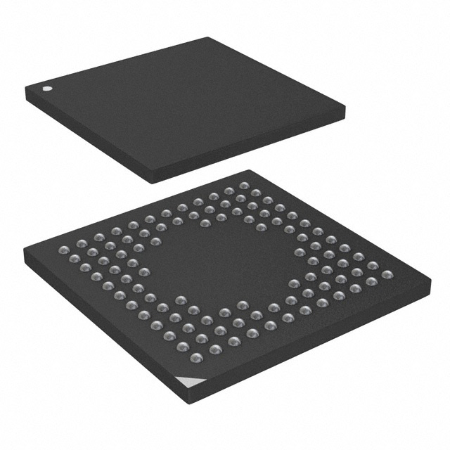
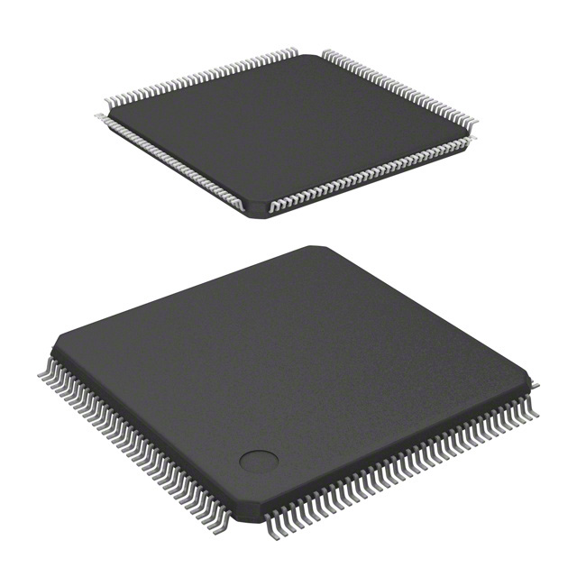
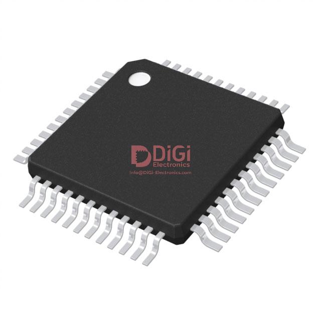
Within the STM32F373xx series, alternative packages—including LQFP64, LQFP100, and UFBGA100—enable tailored scaling for system expansion, accommodating more I/O channels or increased onboard flash memory. These variants retain a consistent electrical and peripheral framework across package types. This compatibility means leveraging shared middleware and development toolchains, which greatly reduces time-to-market for derivative designs or families of modular hardware.
In practice, robust system integration hinges on harmonizing package selection with both mechanical limitations and projected connectivity needs. The LQFP form factor merges ease of inspection with automated assembly reliability; however, the UFBGA100 variant, with its finer pitch and reduced profile, prioritizes ultra-dense layouts but demands advanced optical inspection and precise soldering controls. Experienced designers recognize the necessity of rigorous design rule checks and cross-referencing manufacturer-provided layout examples, thereby favoring predictable results in signal integrity and manufacturability. Ultimately, the STM32F373CBT7’s well-documented mechanical assets and standardized package strategy create a versatile foundation for small-scale embedded systems, facilitating a blend of agility in prototyping and robustness in volume production.
Potential equivalent/replacement models for STM32F373CBT7 STMicroelectronics
The selection of a substitute for the STM32F373CBT7 from STMicroelectronics demands a methodical approach focused on hardware compatibility, feature parity, and architectural nuance. Within the STM32F373xx lineage, models like STM32F373CCT7 and STM32F373RCT7 provide alternative flash and RAM capacities as well as different package footprints. Utilization of these variants supports scaling for applications with fluctuating memory demands or spatial constraints while maintaining peripheral congruence. The close architectural overlay across the F373xx family streamlines firmware migration, minimizing code adaptation and validation overhead.
For expanded analog subsystem capabilities or elevated computational throughput, adjacent products in the STM32F3 portfolio, such as STM32F303 or STM32F334, offer a differentiated set of high-resolution ADCs, advanced comparators, and extended timer functionalities. When fine-tuning signal acquisition systems or digital power conversion designs, the nuanced analog front-end enhancements of these models frequently enable direct performance gains without substantial board redesign. Practical cross-evaluations demonstrate that minor variations in register maps and hardware abstraction layer support can be bridged within typical project timelines, conditional upon attentive review of reference manuals and toolchain compatibility.
In pursuits where ultra-low-power operation is instrumental—battery-powered instrumentation, for example—the STM32L4 series emerges as a viable migration target. This family integrates aggressive sleep modes and efficient wakeup logic, reducing quiescent current footprints. Importing designs from the F373 line to the L4 series generally requires heightened scrutiny toward voltage domains and clock source configurations, but the underlying ARM Cortex core similarities mitigate major porting risks. Empirical findings suggest that migration success correlates strongly to matching peripheral sets and sustaining well-defined signal-timing specifications.
Pin assignment and electrical interface alignment remain non-negotiable. Pinout differences and peripheral mapping must be cross-validated against the original schematic, especially for modules relying on precise ADC channels and timer outputs. Subtle incompatibilities in I/O drive strength or analog reference routing can cascade into systemic errors post-migration if not proactively identified at the design review phase. Implementing matrix-based comparison tools streamlines identification of mismatches and supports comprehensive validation of direct-swappable candidates.
In synthesizing optimal replacement strategy, the emphasis lies in leveraging family continuity when available, then branching selectively into adjacent series for cases where analog sophistication or power economy defines the application envelope. The strategic use of datasheet cross-referencing, evaluation board prototyping, and automated pin/peripheral comparison substantially derisks migration, reducing iterative hardware cycle counts and accelerating end-system reliability objectives. Such methodical engineering discipline fosters robust outcomes and future-proofs system designs against supply uncertainties or evolving performance requirements.
Conclusion
The STM32F373CBT7 microcontroller represents a refined intersection of computational efficiency and analog-digital integration. Architected with an ARM Cortex-M4 core operating at up to 72 MHz, the device delivers deterministic performance suitable for time-critical control loops and signal processing tasks. Its floating-point unit, coupled with a rich set of mathematical instructions, enables precise operations in embedded control and sensor fusion scenarios. The microcontroller’s embedded memory hierarchy—comprising up to 128 KB Flash and 32 KB SRAM—streamlines code execution and supports robust data handling, facilitating real-time responsiveness even under multi-threaded workloads.
Analog subsystem capabilities distinguish this platform within the STM32F3 series. Dual 16-bit sigma-delta ADCs, high-resolution DACs, and advanced comparators empower designers to address complex measurement environments and mixed-signal processing pipelines. The programmable gain amplifiers extend interface flexibility for diverse sensor inputs, allowing seamless adaptation to high-precision data acquisition and industrial automation signals. Integrated hardware filters further offload signal conditioning from software, enhancing overall system throughput.
Digital connectivity and peripheral integration within the STM32F373CBT7 expand its application framework beyond conventional microcontroller boundaries. Native support for USB, CAN, and multiple USART/SPI/I2C channels creates a fertile ground for interoperability with external modules, fieldbus networks, and custom expansion boards. Tailored GPIO mapping and timer resources provide granular control over timing-sensitive functions, including motor drives, pulse generation, and communication protocols. The device’s scalable pin count and compact LQFP48 packaging enable optimal utilization in space-constrained circuit layouts without sacrificing feature accessibility.
Operational reliability is augmented through low-power modes, voltage detection mechanisms, and a comprehensive clock management system. Sophisticated power management allows for dynamic adjustment of core frequency and peripheral activity, effectively balancing performance with energy consumption in battery-powered and low-duty-cycle applications. Attention to package thermal characteristics and EMI resilience ensures sustained operation across harsh industrial and medical environments, where stability and longevity are essential parameters.
System-level integration demands careful evaluation of resource partitioning, peripheral assignments, and firmware abstraction layers. Leveraging the modular configuration tools provided within the STM32 ecosystem substantially accelerates the prototyping and validation cycles. In deployment scenarios, real-world testing reveals the impact of peripheral cross-interference, timing skews, and analog reference drift—insights that drive refinements in PCB layout, shielding, and decoupling strategies. Experiences with edge cases underscore the value of comprehensive error handling routines and watchdog schemes, reinforcing the platform’s suitability for mission-critical applications.
Selection strategies benefit from prioritizing scalability, longevity of supply, and ecosystem support. The STM32F373CBT7, with its vendor-committed longevity program, ensures uninterrupted supply, minimizing redesign risks and supporting sustained field deployment. The extensive software library resources and third-party middleware availability streamline integration into advanced automation, medical instrumentation, and consumer electronic designs. Early consideration of application-specific needs—such as analog channel count, real-time networking, and hardware security—enables tailored configuration, optimizing resource allocation for long-term operational excellence. The microcontroller’s architecture, balanced between analog performance and digital connectivity, creates a solid foundation for next-generation embedded solutions.