 >
>


Product overview: STM32F373CBT6 microcontroller
The STM32F373CBT6 microcontroller, positioned within the STM32F3 series, centers around balancing computational throughput, analog integration, and system connectivity within a constrained form factor. Leveraging the ARM Cortex-M4 core, it brings a hardware-efficient DSP engine and single-precision FPU, optimizing both time-critical signal processing and resource-aware embedded computation. Integration at the silicon level encompasses 128 KB of Flash and 24 KB of SRAM, with deterministic access times, enabling both code density and reliable real-time behavior in event-driven systems.
Analogue subsystems within the STM32F373CBT6 remain a key differentiator, offering multiple high-resolution 16-bit Sigma-Delta ADCs, along with three 12-bit DACs and fast analog comparators. These resources permit seamless sensor interfacing, active signal conditioning, and support for closed-loop control strategies directly on-chip. Modularized analog blocks facilitate changes to signal paths without extensive rework at the board level—a yield-accelerating advantage in prototyping and rapid iteration cycles, especially apparent in motor drive, power management, and instrumentation applications.
The peripheral matrix supports a diverse range of I/O protocols, including I2C, SPI, USART, CAN, and USB 2.0 Full-Speed, allowing flexible topologies from single-unit edge nodes to interconnected gateway architectures. Notably, the availability of advanced timers with high-resolution PWM outputs and dead-time insertion promotes precision in motor control and digital power conversion. For engineers managing complex signal paths or distributed sensors, synchronized analog triggering and programmable interconnects minimize software overhead while containing latency and jitter.
Application deployment benefits from the device's compact LQFP-48 package, easing PCB routing and minimizing parasitic effects in signal-sensitive layouts. In real-world implementations, deployment in tightly coupled PCB environments underscores the utility of robust ESD protection and multiple power domains, where noise resilience is directly attributable to ST’s segmented supply management. Engineering experience supports the use of on-chip oscillators and flexible system clocking for rapid bring-up and EMI-aware board design, with the backup domain enhancing low-power data retention through RTC integration.
A defining aspect is the convergence of deterministic DSP, versatile analog interfaces, and adaptable connectivity, which reduces reliance on discrete components and shortens embedded design cycles. In iterative development, firmware-level diagnosis leverages the Cortex-M4’s hardware breakpoints and trace capabilities—a catalyst for shortened debug and validation steps. An overlooked yet profound benefit lies in the nuanced calibration options for analog peripherals; field recalibration via firmware allows long-term drift correction, extending device lifecycles in high-reliability applications.
Overall, the STM32F373CBT6 deploys as an analog-intensive, compute-optimized microcontroller suited for tightly-integrated real-time systems, where the intersection of analog fidelity and processing determinism is paramount. This convergence fundamentally changes the design calculus, favoring platform consolidation and long-term scalability within demanding, application-specific environments.
Core architecture and processing capabilities of STM32F373CBT6
The STM32F373CBT6 embeds a single-core ARM Cortex-M4 processor running at frequencies up to 72 MHz, positioned to address real-time embedded control scenarios with high computational density. This core achieves 1.25 DMIPS per MHz, leveraging hardware acceleration through built-in single-cycle 32-bit multiplication and hardware division units. The inclusion of a hardware floating-point unit (FPU) and an optimized DSP instruction set brings substantial improvements to digital filtering, signal conditioning, and fast control-loop implementations, particularly in applications like power conversion and precision analog measurements.
Beneath the core, the memory protection unit (MPU) establishes firm boundaries between program regions, supporting not just safety-critical isolation but also enabling robust multi-threaded firmware architectures. This resource is instrumental in the management of complex embedded software stacks, enforcing privilege separation which mitigates the risk of errant code propagation and runtime faults—a consideration often overlooked in less demanding real-time applications but essential for ISO 26262 and IEC 61508 compliant projects.
Determinism in time-sensitive control scenarios is addressed through the nested vectored interrupt controller (NVIC). The fine-grained interrupt prioritization and low-latency preemption allow engineers to create interrupt-driven architectures where the response time to asynchronous inputs, such as those from ADCs or external comparators, remains predictable. This is heavily utilized in field-oriented control (FOC) for motor drives, where precise timings directly impact torque smoothness and energy efficiency.
Real-time timers, including advanced general-purpose and basic timers with up to 16-bit resolution, offer flexible pulse and interval generation down to the single microsecond. In energy metering and portable instrumentation, these timers synchronize sampling operations, coordinate PWM generation, and sequence high-speed data processing. Custom timer configurations often prove critical when integrating multiple closed-loop controllers, ensuring that system jitter stays well-bounded, especially when the peripherals operate concurrently under high CPU load.
Experience shows that DMA channels, tightly coupled with peripheral events, further offload time-critical data transfers, leaving CPU cycles dedicated to complex signal analysis. Application cases in industrial measurement highlight how this architecture sustains high throughput on multi-channel ADC interfaces without timing overrun, a result hard to replicate with cores lacking these tightly-integrated features.
STM32F373CBT6's architectural design builds on a balance between computational power, flexible interrupt handling, and robust memory partitioning, forming a solid foundation for embedded designs where precise control, high reliability, and real-time response are non-negotiable. Attention to harnessing the FPU and DSP extensions, combined with thoughtful partitioning using the MPU, often delivers superior performance and fault tolerance, reinforcing the effective deployment of advanced control algorithms in cost-sensitive embedded systems.
Integrated memory and data management in STM32F373CBT6
Integrated memory and data management in the STM32F373CBT6 hinge on a coherent architecture that balances non-volatile storage, volatile working space, and automated data transfer mechanisms. Central to this system, the 128KB embedded Flash provides persistent program storage, engineered for cycle endurance and data retention that meet robust industrial expectations. Sector-based organization within the Flash allows for efficient in-application programming with carefully controlled erase and write cycles. Real-world firmware refresh procedures leverage this flexibility to implement dual-bank or rolling update schemes, minimizing system downtime and ensuring safe fallback in case of programming faults.
The internal 24KB SRAM features integrated parity checking at the hardware level, continuously monitoring data integrity without software overhead. In environments prone to electromagnetic interference or subject to temperature extremes, this real-time error detection mechanism has proven indispensable for safeguarding volatile computation states, especially during complex peripheral interactions or multitasking scenarios.
Boot mode configuration introduces operational versatility: selectable paths at reset let the system load factory bootloader for device provisioning, hand off control to a user application, or engage in system-level programming for secure code uploads. Deployments in field-upgradeable systems depend on this mechanism to orchestrate protected firmware updates, utilizing authentication and memory isolation patterns to mitigate risks of unauthorized code injection or bricking.
A 12-channel DMA controller substantiates performance and determinism in data-intensive tasks. DMA orchestrates high-throughput data transfers between memory and peripherals such as ADCs, DACs, USARTs, or SPI interfaces—completely offloading the CPU. This technique removes bottlenecks typical of interrupt-driven designs and greatly improves system responsiveness, a necessity in motor control, sensor signal processing, or communication protocol stacks. Careful mapping of peripheral-DMA linkages, accompanied by priority tailoring and double-buffering schemes, enables designers to maintain predictable latencies even during peak load.
Practical deployments emphasize the interplay between these resources: for example, cyclic sensor acquisition routines use DMA to fill SRAM buffers, with parity logic silently ensuring fidelity, while interrupt-driven tasks execute from Flash. Simultaneously, staged firmware updates rely on dynamic boot mode switching and granular Flash partitioning. Strategic integration of these features not only elevates functional robustness but also supports efficient certification and long-term field maintenance. The core advantage emerges from treating memory and data flow management as a synchronized system rather than as isolated features, enabling scalable performance and resilient design across a wide array of embedded applications.
Power management and low-power features of STM32F373CBT6
The STM32F373CBT6 MCU incorporates a multi-layered approach to power management, tailored for systems where energy efficiency is paramount. Its three principal low-power modes—Sleep, Stop, and Standby—provide granular control over consumption. Sleep mode halts the CPU while retaining oscillator and peripheral functionality, enabling rapid wake-up with minimal latency; in practical usage, this reduces unnecessary cycles during brief inactivity without loss of real-time responsiveness. Stop mode enters a deeper power-down state by suspending oscillators and most clocks, with RAM retention. This mode suits scenarios with intermediate idle durations, such as wireless sensor intervals, ensuring fast recovery upon trigger yet keeping standby energy at a minimum. Standby mode disables all contexts except those necessary for wake-up logic and RTC operation, minimizing current to the microampere level and preserving VBAT-backed data—a strategy essential for metering endpoints or long-term remote deployments where battery longevity is critical.
The core operates efficiently across a 2.0V to 3.6V supply range, facilitating seamless integration into single-cell lithium, dual alkaline, or regulated supply designs. Monitoring infrastructure is robust: the programmable voltage detector (PVD) enables predictive mitigation of brownout incidents by generating interrupts before operational thresholds are crossed, allowing firmware to execute corrective routines or initiate safe shutdown states. Watchdog mechanisms—available both as independent hardware modules and system-driven software timers—guard against unpredictable execution paths or peripheral failure, automating MCU reset in anomalous conditions. Field experience confirms the effectiveness of this redundancy, with lock-up events being intercepted without external intervention, maintaining operational reliability under adverse electrical or thermal stress.
The Real-Time Clock (RTC), powered from a dedicated VBAT pin, persists across main power loss, maintaining accurate timekeeping and supporting scheduled wakeups via alarms or tamper detection. In distributed sensing environments, the RTC’s independence streamlines synchronization tasks. This unlocks advanced scheduling—data collection, transmission, or calibration routines—regardless of supply interruptions, substantially reducing firmware complexity concerning deep sleep recovery and event timestamping. Layered wake-up sources, including external interrupts and RTC-driven alarms, allow designers to tailor responsiveness to specific application protocols, exemplified by appending metering pulses or recognizing threshold violations in a low-power manner.
A nuanced understanding of peripheral clock gating and selective power domain management further refines consumption envelopes. Effective application of these features—such as deactivating unused communication interfaces or leveraging DMA for burst data transfer in low-power modes—yields compounding savings, notably in designs where operational cycles vary dynamically. The true differentiation of the STM32F373CBT6 resides in the seamless transition mechanics between run and retention states: system stability and data integrity are preserved due to atomic register updates and consistent interrupt behavior. This reliability fosters aggressive power management strategies without incurring the risks typically associated with deep sleep architectures. These attributes position the MCU as a compelling solution for energy-constrained systems, supporting scalable application designs that balance performance, autonomy, and lifecycle maintenance.
Oscillator, clocking, and timing features in STM32F373CBT6
Oscillator, clocking, and timing architecture in the STM32F373CBT6 exemplifies a high degree of configurability, accommodating a spectrum of design constraints. The microcontroller integrates multiple clock sources: an external crystal oscillator supporting 4–32 MHz for the system clock, an independent 32 kHz oscillator optimized for the real-time clock domain, and selectable internal RC oscillators at 8 MHz and 40 kHz. The inclusion of a phase-locked loop (PLL) module enables on-the-fly frequency synthesis, permitting refined clock scaling while maintaining jitter performance suitable for precision-centric subsystems.
Selecting between external and internal oscillators requires scrutiny of accuracy, stability, and power consumption. The external crystal, while drawing more current, offers superior frequency tolerance (critical in high-precision timing), whereas the internal RC options, with their fast startup and lower current profiles, excel in rapid wake/sleep cycles and ultra-low-power states. The 32 kHz oscillator serves low-drift timekeeping, enabling consistent RTC operation during power-saving modes. Multi-source clocking, managed via dynamic hardware control registers, enables seamless migration between run and standby states, facilitating real-time adaptation to variable system priorities.
Timing functionality leverages up to seventeen timers distributed across two architectures: two 32-bit units, providing extended range for overflow-free pulse measurement, and a suite of 16-bit timers, ideal for dense, low-latency PWM signal generation and event scheduling. Advanced timer resources enable edge-detection, frequency counting, and input capture modes, tightly integrating with motor control feedback loops and sensor interfaces. Direct Memory Access (DMA) handshake further streamlines timer operation, reducing CPU involvement in repetitive tasks such as DAC waveform synthesis or multi-channel PWM modulation.
Layered clock domain isolation and fine-grained prescaler control foster deterministic timing, crucial for industrial automation protocols and closed-loop motor commutation algorithms. Precision in timer synchronization minimizes phase lag, improving system response fidelity and jitter margins in control systems. PLL-aided frequency multiplication maintains clock integrity, even with variable peripheral loads, ensuring reproducible timing—this proves particularly effective in multi-motor or process automation contexts where event-driven latency is a limiting factor. Subtle clock switchover logic embedded in hardware supports robust failover, minimizing the risk of timing drift in mission-critical scenarios.
Through operational refinement—such as dual-source RTC backup, adaptive prescaler adjustments during workload peaks, and leveraging DMA for timer-based data streaming—the platform achieves resilient and efficient timing management. The architecture’s inherent flexibility encourages design strategies prioritizing accuracy or power, depending on the operational phase, yielding optimized solutions for tasks ranging from precise signal synchronization to energy-conscious sensor sampling. This layered approach not only addresses contemporary automation and control challenges, but also opens avenues for low-cost yet high-performance timing solutions.
I/O and peripheral integration of STM32F373CBT6
I/O and peripheral integration within STM32F373CBT6 is engineered for versatility and real-time performance. The device presents 36 general-purpose I/O pins—expanding to 45 in certain package variants—all designed with 5V tolerance. This high voltage robustness directly simplifies hardware design in mixed-voltage environments, offering seamless interconnection to both legacy 5V logic and modern 3.3V systems without external level shifting. Each I/O supports flexible assignment to peripheral functions, such as SPI, I2C, or USART, allowing dynamic reconfiguration through remapping resources as dictated by application-level demands. This adaptability minimizes board-layer complexity during layout and shortens design iteration cycles.
Mapping all I/Os to external interrupt vectors fundamentally enhances deterministic event handling. The integration with the EXTI module ensures rapid response to asynchronous, real-world events from sensors or user interfaces. Fast peripheral wake-up and low interrupt latency are realized by optimized silicon paths, especially when precise motor control or fail-safe shutdown logic are mandatory.
For capacitive touch and proximity applications, up to 24 dedicated sensing channels are provided. Hardware-level signal separation and noise immune acquisition algorithms allow reliable gesture recognition even in electrically noisy environments. This drastically reduces the software post-processing burden and streamlines the development of cost-sensitive HMI systems. Board bring-up with touch firmware benefits from factory-trimmed calibration and embedded diagnostics, reducing production line tuning and ongoing field returns.
RTC and calendar integration with backup registers extends use into dataloggers and always-on metering, where persistent time-stamping and robust operation through power interruptions are essential. The embedded SysTick 24-bit timer acts as a deterministic heartbeat for both OS kernel tick management and real-time tasks, while facilitating cycle-accurate timing for application profiling and precise temporal boundaries in time-critical control loops.
Peripheral resource breadth and I/O matrix configurability set the STM32F373CBT6 apart when applied to industrial automation, instrumentation, or multi-sensor fusion nodes. The architecture’s inherent flexibility supports iterative prototyping and future-proofing, enabling adaptation to unforeseen specification changes without substantial redesign. Subtle yet significant, the combination of high-voltage tolerant, individually remappable pins and a comprehensive interrupt/event fabric is leveraged in systems demanding both robust electromagnetic compatibility and minimal ISR latency—characteristics foundational to resilient, safety-sensitive embedded deployments.
Analog subsystem and data conversion capabilities in STM32F373CBT6
The STM32F373CBT6 microcontroller integrates an advanced analog subsystem designed for precision measurement and signal processing, distinguishing itself within its performance class. At its architecture’s core is a high-speed 12-bit successive approximation register (SAR) ADC, capable of 1 μs typical conversion time across up to 16 multiplexed channels. This configuration enables rapid, responsive sampling, well-suited for motor control, power monitoring, or real-time signal tracking—applications relying on low-latency analog-to-digital conversion.
Augmenting this, the device employs three 16-bit sigma-delta ADCs (SDADCs), each optimized for high-resolution, low-noise data acquisition. Sigma-delta topology achieves superior dynamic range, making these channels ideal for instrumentation that demands fine granularity, such as medical diagnostics or high-precision sensor systems. The SDADCs support a configurable selection of up to 21 single-ended or 11 differential inputs, efficiently aggregating multisensor data while maintaining signal integrity even at microvolt levels. In practice, leveraging these channels can counteract common-mode disturbance and mitigate quantization errors, provided layout symmetry and reference stability are maintained.
Digital-to-analog conversion is addressed by three independent 12-bit DAC channels, facilitating flexible signal synthesis, waveform generation, or actuation. Their deployment is particularly effective in closed-loop control or calibration scenarios, where tailored analog voltages are required for external peripheral tuning or offset compensation. To exploit their full resolution, careful attention should be given to reference selection and output loading, as precision degrades with reference drift or excessive current draw.
Completing the analog feature set, dual rail-to-rail comparators allow adaptable threshold-based monitoring without sacrifice of input dynamic range. These comparators support window detection and zero-cross detection, functions essential for robust real-time event discrimination in transducer and protection designs. Integrated temperature sensor and reference voltage monitoring further optimize analog performance, supporting active compensation of temperature drift and ensuring converter accuracy throughout operational ranges.
From a design perspective, achieving optimal results with the STM32F373CBT6 analog subsystem requires harmonizing PCB layout, reference routing, and power supply decoupling. Isolating sensitive analog traces, employing Kelvin connections for differential inputs, and utilizing low-ESR decoupling capacitors are best practices to suppress crosstalk and rail fluctuations. The multiplexed structure of the SAR ADC demands sequential timing strategies if maximum throughput is critical without channel-to-channel interference.
Notably, this MCU’s unified analog matrix supports simultaneous operation of the SAR and SD ADCs, allowing the system architect to judiciously allocate high-speed tasks and high-precision measurements without resource contention. Direct memory access (DMA) can further offload CPU overhead during bulk data acquisition, enhancing throughput in sensor fusion or waveform capture applications. The inclusion of robust analog blocks, internally referenced and temperature compensated, provides a foundation for consistent, reliable instrumentation-grade signal conversion within cost-sensitive embedded platforms.
Unified analog and digital configuration, coupled with the flexibility of STM32 peripheral interconnectivity, enables sophisticated application scenarios, from multi-channel data loggers and electrochemical analysis equipment to closed-loop medical instrumentation and advanced motor drives. In essence, the STM32F373CBT6 exemplifies how a thoughtfully architected analog subsystem can catalyze high-performance design, condensing instrumentation capabilities into a compact, software-defined system.
Programmable communication interfaces in STM32F373CBT6
Programmable communication interfaces within STM32F373CBT6 are architected for robust system integration across diverse application domains. At the protocol level, the controller area network (CAN 2.0B) peripheral enables deterministic, low-latency message exchanges ideal for industrial automation, distributed control, and fault-tolerant networks. Its hardware-based filtering and prioritized arbitration minimize software overhead and ensure real-time responsiveness even under heavy bus loads.
The USB 2.0 Full Speed interface delivers seamless host-device connections for firmware updates, data logging, and peripheral expansion. Leveraging the embedded USB stack, developers can realize composite devices or streamline bootloaders while ensuring compliance with standard USB classes. This facilitates rapid prototyping and field firmware upgrades without external programmers.
Serial connectivity is covered by three independent USARTs, each supporting a spectrum of communication modes. Synchronous operation enables master/slave clocked serial streams for legacy protocols, while ISO/IEC 7816 support makes the platform suitable for smart card interfacing in secure authentication systems. LIN and IrDA peripheral modes provide flexible scalability from low-cost automotive or appliance networks to contactless data exchange, and wakeup functionalities offer power-saving mechanisms vital in battery-powered instrument clusters. The auto baud rate feature simplifies interoperability with variable-rate serial links, reducing configuration errors during deployment.
The triad of SPI interfaces each supports bit rates up to 18 Mbps, allowing the STM32F373CBT6 to sustain high-throughput links to external memory, high-speed ADCs/DACs, or display controllers. Multi-SPI operation in redundant or parallel configurations can address bandwidth or reliability constraints in data acquisition and sensor fusion platforms.
For complex board designs deploying multiple digital sensors or configuration EEPROMs, the twin I2C controllers—compatible with Fast Mode Plus standards—provide flexibility for device population and scalability. The increased clock rate yields reduced polling latency in interrupt-driven architectures, enabling responsive HMI (human-machine interface) or power management loops.
Application-specific integration is further extended by HDMI-CEC support, simplifying communication between multimedia nodes in home automation or consumer AV products. The I²S interface, optimized for low-jitter clock synchronization, underpins high-fidelity digital audio transport, suitable for portable audio, instrumentation, or active noise control.
In practice, leveraging the STM32Cube CMSIS driver stack alongside suitable middleware enables rapid enablement and validation of these interfaces. Resource contention is minimized through judicious DMA and interrupt prioritization, and simultaneous multi-protocol communication can be orchestrated by configuring peripheral remapping in the system configuration block. This enables flexible PCB layout options and the reuse of scarce microcontroller pins in space-constrained designs.
From an engineering perspective, such a breadth of on-chip interfaces empowers architectural decisions around protocol selection, partitioning of time-critical tasks, and the reduction of external component count. It also unlocks iterative prototyping and diagnostic instrumentation, accelerating design validation cycles. The level of integration in the STM32F373CBT6 not only enhances electrical interface versatility but also contributes to design resilience and scalability in evolving embedded ecosystems.
Package, mounting, and environmental attributes of STM32F373CBT6
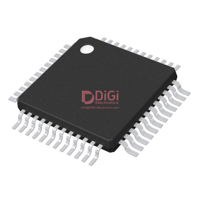
The STM32F373CBT6 microcontroller features a compact 48-pin LQFP package with a 7 × 7 mm footprint, optimizing PCB real estate for constrained layouts and high-density systems. Its surface-mount design seamlessly integrates within automated reflow assembly lines, reducing manual intervention and supporting high-throughput production. Under extreme operating conditions, the –40°C to +85°C temperature range accommodates environments with significant thermal cycling, enabling deployment in control systems, sensor hubs, and automotive subsystems where reliability and tolerance to fluctuations are critical.
The device exhibits robust electrical integrity, highlighted by comprehensive ESD and EMC protections. This mitigates transient disturbances in electrically noisy installations, guarding sensitive digital and analog circuits against surge events and coupling effects. The supply voltage flexibility, with Vcc/Vdd operational from 2.0V to 3.6V, grants designers greater leeway in board-level power sequencing and enables cost-effective selection of regulators and batteries, advancing adaptability across diverse platforms—ranging from battery-powered sensor nodes to automotive ECUs.
Manufacturing considerations are addressed through RoHS3 compliance, supporting environmental responsibility and regulatory acceptance for global distribution. The Moisture Sensitivity Level classification (MSL 3, 168 hours), validated for reflow soldering, underscores stability against delamination and popcorning—key failure mechanisms in high-humidity assembly environments. When provisioning volume production, careful management of floor life and storage conditions for the unmounted devices becomes essential to safeguard reflow yield and long-term reliability.
Integrated trace and debug support transforms the development cycle, providing non-intrusive access to real-time system behavior and checkpoint capabilities during production test. These embedded features reduce the necessity for external instrumentation, streamlining validation cycles and accelerating fault isolation under tight schedules.
A notable aspect is the convergence of mechanical, electrical, and ecological criteria in the STM32F373CBT6, where packaging solutions are not treated as discrete subjects but as interlocking factors in achieving resilient designs. For example, experience shows that early attention to pin arrangement and thermal path in layout minimizes hotspots and EMI, not only meeting datasheet ratings but elevating system robustness. This subtle integration of multilayered considerations—physical, electrical, and environmental—positions the STM32F373CBT6 as a sophisticated choice for designs demanding both high reliability and manufacturability.
Potential equivalent/replacement models for STM32F373CBT6
Within the STM32F373 portfolio, device interchangeability centers on shared core architecture and compatible pinout configurations. Direct alternatives such as STM32F373C8, STM32F373CB, and STM32F373CC emphasize memory differentiation—primarily in Flash and RAM capacities—without altering fundamental peripheral sets or signal integrity. This enables seamless scalability during late-stage prototyping, where migrating between SKUs preserves firmware investment and PCB layout, minimizing design churn.
Pinout-consistent options extend into broader package offerings, including 64-pin and 100-pin LQFP, as well as UFBGA formats. Models like STM32F373RB/VB/RC/VC map the same core functions across more pins, unlocking richer interface density for applications requiring extended connectivity or higher I/O granularity, such as industrial control or advanced instrumentation. Here, functional symmetry ensures that migration between form factors remains bounded by predictable constraints—chiefly manifested in I/O assignment, power plane considerations, and thermal envelope adaptation.
A feature-focused approach identifies variants within the family that supplement base functionality with upgraded analog peripherals, faster ADCs, or enhanced timer arrays. Selection leverages direct BOM optimization, supporting cost-driven substitutions or performance upgrades without wholesale platform redesign. This approach favors modular hardware design principles, enabling targeted evolution of system capabilities as requirements shift.
Practical development often reveals nuances in electrical characteristics between memory densities and package types, particularly under boundary operating conditions like elevated ambient or transient loads. Engineers systematically analyze datasheet tolerances and errata, iterating test regimes to ensure functional parity during model swaps. Embedded software compatibility is preserved by the shared ARM Cortex-M4 core and a uniform peripheral mapping, streamlining project timelines and reducing validation effort.
The core insight is that the STM32F373 series, with its tightly-aligned SKUs, fosters a configuration-driven hardware design strategy. By treating device selection as a parametric constraint within well-defined architectural boundaries, engineers gain control over cost, footprint, and feature set—frequently unlocking latent flexibility in system deployment.
Conclusion
The STM32F373CBT6 microcontroller distinguishes itself through a highly integrated architecture tailored for real-time data acquisition and processing. Central to its capability is the ARM Cortex-M4 core, equipped with a floating-point unit, which streamlines digital signal processing and complex control algorithms. This hardware foundation ensures deterministic response times demanded in measurement, control, and safety-critical applications. The inclusion of high-resolution, multi-channel analog-to-digital converters, fast analog comparators, and programmable gain amplifiers positions the device at the forefront for handling sensor-rich environments and precision instrumentation, minimizing external component count and PCB complexity.
Connectivity within the STM32F373CBT6 is addressed through configurable interfaces, including SPI, I2C, USART, and CAN, enabling seamless integration into heterogeneous system environments. The combination of these digital communication protocols with integrated analog features supports direct connection to industrial transducers, communication modules, and motor control platforms, reducing both latency and system overhead. Integration of advanced timers and flexible PWM units further extends applicability to power management, digital power supplies, and closed-loop control, where subtleties such as dead-time insertion and high-frequency waveform generation are mission-critical.
System robustness is further reinforced by embedded safety features, such as clock security systems, watchdog timers, and brown-out reset circuits, which safeguard operation against transient disturbances and ensure compliance with industrial reliability standards. Internal error detection mechanisms and flexible boot configuration make the STM32F373CBT6 suitable for deployments requiring field updates, redundancy, and secure firmware loading. These mechanisms, coupled with a proven firmware ecosystem and extensive reference designs, translate into lower development risks and shortened validation cycles.
Deploying the STM32F373CBT6 in system designs reveals its strengths in precise real-time control—examples include three-phase metering devices, portable medical analyzers, and fieldbus-connected industrial sensor hubs, where low-noise analog front-ends and deterministic actuator control are non-negotiable requirements. In scenarios with escalating channel density or processing demands, the broader STM32F3 family provides straightforward paths for scale-up or pin-compatible migration, protecting upfront investment in hardware and software assets.
Evaluating device alternatives within the same portfolio or from competing vendors requires critical assessment of analog fidelity, software ecosystem maturity, and logistical support. The STM32F373CBT6 consistently delivers advantages in signal integrity and peripheral cohesion, enabling differentiated solutions where system cost, PCB space, and regulatory certification timelines are key constraints. Leveraging such an architecture optimizes not just the immediate design, but future-proofs platforms against evolving compliance and performance standards.