 >
>


Product overview: STLED25JR STMicroelectronics IC LED driver regulator PWM
The STLED25JR LED driver IC delivers a tightly integrated solution for powering high-brightness white LEDs across demanding display platforms. At its core, the device features a step-up DC-DC converter architecture that elevates supply voltage, enabling the consistent current delivery required for uniform backlighting in multi-LED configurations. The inclusion of parallel high-side current sources supports precise LED current balancing, mitigating dimming discrepancies and enhancing overall luminance homogeneity—critical parameters for visual performance in high-resolution LCD displays.
Its compact footprint—achieved through advanced flip-chip packaging at 1.4 x 1.8 mm—satisfies stringent miniaturization mandates typical of portable electronics. This packaging supports low parasitic resistance and inductance, directly benefiting high-frequency PWM operation and delivering improved electromagnetic compatibility. Engineered to control up to ten LEDs simultaneously, the STLED25JR offers scalable wiring schemes, easing layout constraints and supporting flexible display design topologies. The device’s step-up DC-DC conversion efficiency not only limits thermal dissipation but aligns with the need to prolong battery life, especially within low-profile handhelds such as cellular phones and PDAs.
On the control side, the integrated PWM regulation mechanism provides dynamic brightness adjustment. The linearity and response time of the PWM circuitry ensure seamless transitions in illumination, critical for applications where rapid visual feedback is required. During implementation, attention must be given to the quality of the input decoupling and output filtering to maximize noise immunity and ensure stability across varying load demands. Practical deployments have revealed that careful tuning of switching frequency and careful selection of inductor and output capacitor values directly impacts EMI profiles and maximizes conversion efficiency—an aspect not sufficiently emphasized in many reference designs.
One core insight is the advantage conferred by high-side current regulating topology. By eliminating ground bounce and simplifying thermal management, this approach allows placement flexibility for LEDs within the device, streamlining PCB routing. Furthermore, selective activation of LED channels via external logic allows for adaptive display dimming patterns, integrating seamlessly into intelligent display modules seeking localized brightness optimization.
In operational scenarios, the STLED25JR demonstrates exemplary reliability under fluctuating ambient conditions, with robust undervoltage and overcurrent protection. The driver’s tight current regulation tolerances significantly reduce ghosting effects, a perennial challenge in backlight matrix arrangements. This fosters clearer contrast and prolongs service intervals for display modules. The synthesis of efficient power topology, flexible control logic, and a compact form factor belongs to a category of LED drivers capable of driving next-generation human-machine interfaces, where display clarity, energy efficiency, and board-level integration converge as competitive priorities.
Key features and performance metrics of STLED25JR STMicroelectronics
Among the distinguishing attributes of the STLED25JR from STMicroelectronics is its highly integrated step-up converter, engineered to handle input voltages spanning from 2.3 V to 5.5 V. This input voltage flexibility enables robust performance in battery-driven environments, where voltage fluctuations and protection against deep discharge are critical. The on-chip power stage allows seamless regulation of output even under variable supply conditions, ensuring system designers can exploit maximum battery capacity without compromising display consistency or system reliability.
The architecture features five output channels, each capable of high-side current sourcing to facilitate direct LED connection. This topology allows two LEDs to be arranged in series per channel, streamlining PCB layout and minimizing interconnect losses. The cumulative drive capacity—a notable 125 mA—supports both moderate- and high-brightness applications, giving engineers latitude in configuring their backlighting or indicator arrays for diverse luminance demands. Channel-to-channel independence also aids in implementing intricate lighting effects or segment control in sophisticated display modules.
Efficiency metrics reach up to 86% at a 100 mA output load, a mark achieved through optimized switching and bias circuitry. This translates to minimal thermal dissipation, reducing the need for ancillary cooling measures and directly supporting compact, energy-constrained products. Experience with real-world implementations highlights how such efficiency not only extends operational lifetime in portable devices but also simplifies compliance with stringent thermal design limits in stacked or encapsulated assemblies.
Precise current control constitutes another core strength. With ±7.5% accuracy across the full operating range, the device mitigates perceptible variation in brightness and color critical for multi-LED arrays—particularly in edge-lit displays or indicator panels demanding uniformity. This performance stems from both high-stability reference design and precision current mirror technology internal to each channel, simplifying circuit calibration and maintaining consistent display performance across the product lifecycle.
Pulse-width modulation (PWM) dimming support is implemented with selectable frequency bands and automatic shutdown functionality. This mechanism enables designers to tune LED brightness to accommodate variable ambient lighting conditions or power-saving states without introducing perceptible flicker or waveform artifacts. The shutdown feature ensures negligible standby current, making the IC exceedingly suitable for always-on consumer and industrial interfaces.
In practical LED matrix system deployments, leveraging the STLED25JR's combination of flexible input handling, tightly controlled output, and high efficiency leads to tangible benefits. For example, in wearable devices or compact instrumentation clusters, the reduction in both active and quiescent power translates into smaller battery footprints and extended recharge intervals. Additionally, the channel configuration permits nuanced dimming schemes, accommodating both static and animated lighting effects that enhance user interface appeal without sacrificing electrical or thermal headroom.
Strategically, these features position the device as a building block for next-generation HMI systems, where size, longevity, and visual performance reciprocally define market acceptance. Integrating this device into modular design flows accelerates development cycles, especially when interoperability with standard microcontroller PWM outputs is required, as the STLED25JR’s interface design supports direct, low-latency digital control. This seamless interaction, coupled with the device’s inherently robust efficiency and accuracy, underscores its suitability for applications ranging from intelligent portables to automotive dashboards, substantiating its reputation for versatile, reliable LED driving in space- and power-limited environments.
Functional architecture of STLED25JR STMicroelectronics
The STLED25JR from STMicroelectronics leverages a tightly integrated functional architecture to address the demanding requirements of medium-scale multi-channel LED applications. At its core, the device employs a fixed-frequency boost DC-DC converter, which elevates input voltage high enough to satisfy the demands of all connected LEDs regardless of their collective forward voltages. This supply topology is directly coupled to five parallel linear current sources, which are optimized to deliver precise, channel-specific current regulation. By grouping these sources into two independent blocks—channels 1–3 and channels 4–5—using separate enable controls (EN13 and EN45), the architecture grants significant flexibility for dynamic lighting scenarios, such as adaptive backlighting or segmented display control, with minimal firmware complexity.
A key innovation lies in the automatic output voltage regulation mechanism. This system ramps the output to precisely 100 mV above the forward voltage of the highest-loaded channel. Such close tracking minimizes dropout across the linear regulators, curbing both power dissipation and thermal stress. This design choice extends operational headroom, particularly beneficial when the number or type of LEDs per string varies due to design constraints or supply variation, making the solution robust against real-world hardware tolerances.
Integrated self-diagnostic features underpin the reliability of the STLED25JR in complex matrices. The internal logic continuously scans for both open-circuit and short-circuit events. When an abnormality is detected, the affected channel is autonomously bypassed or disabled. This preemptive isolation is executed without requiring external microcontroller intervention, ensuring service continuity for unaffected channels and preventing cascading failures. Such granular fault handling is critical for systems where uptime and safety are paramount, such as automotive or industrial lighting, where an isolated fault should not propagate system-wide.
In practice, the channel independence paired with immediate fault management simplifies PCB routing and enhances thermal distribution. It allows for aggressive layout optimization by reducing reliance on external protection circuitry and facilitating tighter group control, reducing the load on the main control unit. The transparent separation of dimming streams also accelerates recalibration or adaptation routines, as specific LED groups can be reconfigured or replaced without disrupting the entire load matrix—a subtle but significant enabler for maintenance-heavy systems.
Examining field behavior, the combined use of fixed-frequency switching, precise voltage tracking, and autonomous protection manifests in stable brightness output even in environments with fluctuating supply or ambient conditions. Subtle improvements in energy efficiency and reduced board thermal gradients can be traced directly to the adaptive linear regulation and channel-level protection logic, distinctively positioning the STLED25JR for scalable, low-maintenance lighting designs where reliability and modularity drive long-term success.
Electrical characteristics and efficiency benchmarks of STLED25JR STMicroelectronics
The STLED25JR from STMicroelectronics exemplifies robust electrical characteristics tailored for demanding mobile and display applications. Its operational envelope spans ambient temperatures from -30°C to 85°C, ensuring that circuit stability and output consistency are preserved both in consumer and industrial environments. This resilience is anchored in a topology that tightly regulates output voltage (V_OUT up to 7.5 V) from low supply voltages (V_IN = 3.7 V), preventing fluctuation during transients and maintaining integrity under thermal stress.
Low quiescent current during shutdown modes sets a benchmark for energy conservation in battery-driven systems. This characteristic directly extends device runtime—especially critical in scenarios where displays idle for extended periods. The architecture achieves minimal leakage through optimized control logic and pass element design, demonstrating a clear engineering advantage for wearables and portable electronics with stringent endurance requirements.
A salient feature lies in precise channel-to-channel current matching. Within multi-output topologies, this capability ensures uniform current distribution, mitigating luminance variance that can degrade visual quality. Such precision emanates from finely tuned feedback control loops, leveraging accurate sensing and compensation strategies to balance channels even as temperature or loading conditions change. The result is homogenous illumination across complex display matrices, reducing the need for post-manufacturing calibration.
Efficiency performance is sustained above 85% across the entire load range, both under light and heavy loads. The device maximizes conversion by minimizing conduction and switching losses, with synchronous rectification and adaptive switching strategies. In field deployments, this minimizes heat generation and further protects battery longevity, permitting higher brightness settings or longer operation between charges.
PWM dimming linearity, maintained from ultra-low 0.39% to full 100% duty cycles, facilitates fine-grained brightness control. The driver’s internal timing circuitry accurately replicates input signals, avoiding artifacts such as flicker or non-uniform transitions. This linear response enhances the user experience by enabling seamless adaptation to ambient conditions or content requirements, supporting advanced technologies like HDR displays and dynamic backlighting.
Practical integration of the STLED25JR often reveals the value of system-level design choices: PCB layout must minimize voltage drop and thermal hotspots to capitalize on the device’s efficiency and current matching. Application scenarios benefiting most are those with multi-zone LED arrays and high-precision visual requirements, where component selection plays a direct role in meeting certification or ergonomic standards. Leveraging such devices, the design window for ultra-thin, high-performance portable displays is broadened, enabling differentiated consumer products with minimal power trade-offs.
A unique aspect of the STLED25JR’s design is its capacity for seamless scaling; tuning for extended output channels or higher peak currents is implemented without compromising the core metrics of efficiency or matching. This confers flexibility for future-proofed designs, accommodating evolving market demands in display and lighting technologies. The device thus represents a convergence of advanced regulation, low-power operation, and precision control, engineered to drive the next generation of high-efficiency visual systems.
Operational modes and protection mechanisms of STLED25JR STMicroelectronics
The STLED25JR from STMicroelectronics implements a robust control architecture tailored for high-reliability LED driving. At its core, the device orchestrates power delivery through four operational states: shutdown, PWM soft start, PWM normal, and run hold. Shutdown mode minimizes quiescent current, facilitating energy efficiency and prolonging system longevity during idle periods. PWM start activates a controlled ramp-up of drive current, mitigating transient stress on both LEDs and power circuitry. This gentle engagement is crucial for preserving emitter lifespan, especially in densely packed lighting assemblies. Transitioning to PWM normal mode, the controller stabilizes current output, leveraging closed-loop feedback to suppress variations induced by supply irregularities or thermal drift. The run hold phase, a brief extension after power-down request, maintains output voltage momentarily, enabling graceful power-down and preempting data loss in tightly timed applications.
Embedded protection mechanisms frame the device's resilient operational footprint. An undervoltage lockout circuit intervenes with precise hysteresis, safeguarding against supply dips that could corrupt state or induce erratic performance. Thermal protection trips at 150°C, preemptively disabling output and reverting only after a safe margin (135°C), providing immunity against ambient extremes and dissipating heat buildup from prolonged high-drive scenarios. Open LED detection circuitry actively identifies load discontinuities, isolating affected channels to prevent hazardous floating voltages and systemic imbalance. Output pin overvoltage protection clamps transients exceeding 9.3 V, substantially reducing vulnerability to back-EMF or poorly-matched external components. In instances of LED channel shorting—common in arrayed panel systems—the device autonomously disconnects offending paths, averting cascade failure and maximizing uptime.
Application experience indicates these layered protections interact synergistically, reducing field maintenance demands and eliminating many failure modes associated with high-density LED matrices. Systems incorporating STLED25JR routinely exhibit tighter parameter consistency across temperature and aging profiles, a direct result of the device's diagnostic logic and self-healing behaviors. Notably, the channel isolation mechanisms have proven invaluable in large-scale installations, where single-channel faults previously escalated to full-system outages. The combination of precise hysteresis in undervoltage response and credible thermal management expands viable operating regions in commercial lighting, architectural displays, and industrial vision platforms. Architectural decisions within the controller imply a design philosophy favoring autonomous fault handling, minimizing the need for external microcontroller intervention even across extended deployment cycles.
Through these mechanisms, the STLED25JR stands as a highly integrated solution. The interplay between mode transitions, fault detection, and recovery circuits points toward an evolution in LED driver reliability—advancing beyond simple protective cutoffs to intelligent, event-sensitive control. The resulting operational agility, steady-state performance, and tolerance to real-world perturbations underscore its suitability for mission-critical and distributed lighting networks.
Application guidelines for STLED25JR STMicroelectronics
Application of the STLED25JR from STMicroelectronics hinges on precise external component selection and PCB layout optimization to harness the device’s full performance envelope. The inductor is a core determinant of system reliability; deploying a 4.7 μH inductor with an adequate saturation current rating is imperative. Selection should be rooted in accurate peak current estimation under worst-case load, preventing magnetic saturation that would induce ripple overshoot and long-term thermal stress. Inductor core material and construction further influence EMI mitigation, thermal dissipation, and long-term stability, with molded or shielded types providing measurable improvements in compact, noise-sensitive assemblies.
The quality and electrical profile of input and output ceramic capacitors directly impact transient suppression, output voltage integrity, and converter stability margins. Capacitors must offer low equivalent series resistance (ESR) to suppress high-frequency switching noise and prevent feedback loop oscillation. The baseline specification—minimum 1 μF for input and 4.2 μF for output—should be seen as an entry point. Field measurements suggest that, in environments with dynamic loads or significant voltage dips, incremental capacitance buffers further flatten voltage excursions and extend operating tolerance. Capacitor placement is equally decisive; traces must be as short and wide as fabrication allows, with the input capacitor positioned immediately adjacent to the VIN and GND pins. This approach constrains parasitic inductance and reduces loop impedance, conferring resilience against voltage transients.
PCB layout not only dictates electrical performance but also influences thermal management and EMC. Current-carrying traces linking the inductor, capacitors, and the STLED25JR must be dimensioned to minimize voltage drop and loop area. Employing ground planes beneath the IC zone reduces inductive coupling and provides a stable reference for sensitive analog nodes. Strategically separating noisy switching nets from feedback pathways further enhances regulation fidelity and protects against radiated emissions. Careful via stitching under return paths can appreciably lower impedance, particularly in multi-layer designs.
Operational experience highlights the interplay between theoretical design and real-world robustness. Component derating, beyond datasheet minima, consistently yields improvements in system lifetime and resistance to atypical operating disturbances—especially in mission-critical or temperature-variable applications. Conservative approach to passive sizing, together with meticulous PCB routing, consistently results in reduced RMA rates and fewer field failures. Advanced simulation followed by bench-validation of the power stage often reveals subtleties in inductor and capacitor interactions, guiding targeted layout refinement or passive selection.
An overarching insight is that the STLED25JR’s efficiency and long-term reliability are strongly correlated with the depth of attention paid to passive quality and spatial arrangement. The device’s performance ceiling is ultimately set not just by internal silicon, but by system-level discipline in component and layout engineering.
Mechanical and packaging details of STLED25JR STMicroelectronics
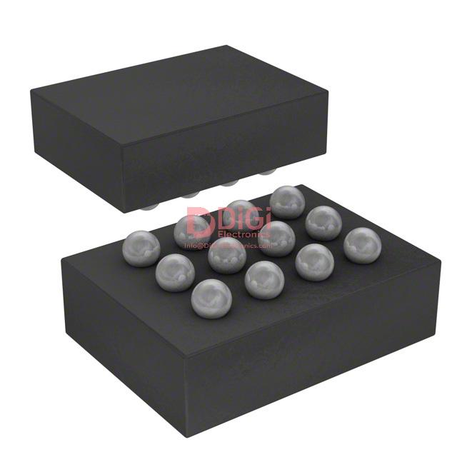
The STLED25JR from STMicroelectronics exemplifies modern miniaturization strategies with its 12-bump chip-scale package, featuring a precise 0.4 mm pitch and an ultra-compact 1.4 x 1.8 mm profile. The underlying bump configuration directly addresses the need for dense integration in portable electronics, where board real estate is at a premium and form-factor constraints drive package reduction. By leveraging fine-pitch interconnects and minimized package outlines, layout engineers can optimize signal routing and component placement within severely limited system dimensions.
The mechanical layout supports streamlined automated handling through a standardized tape-and-reel format. This significantly improves pick-and-place accuracy and throughput during high-volume SMT assembly, mitigating risk of package misalignment and enabling reliable solder joint formation. STMicroelectronics provides detailed reference footprints and mechanical documentation, which are critical in DFM (Design for Manufacturability) analysis and in achieving robust process compatibility across diverse PCB stackups.
Thermal management is intrinsically considered at the package level. The compact geometry of the STLED25JR, coupled with efficient bump distribution, enhances thermal dissipation, allowing designers to maintain junction temperatures within safe operational bounds even when deployed in dense assemblies. The low package height further enables stacking or placement beneath enclosure elements such as display backplates or battery shields, maximizing design flexibility in constrained architectures.
ECOPACK® compliance introduces proactive measures in sustainable sourcing, lead-free processing, and material selection. Meeting these criteria can facilitate qualification for international environmental standards without additional engineering overhead, reducing the risks associated with regulatory delay. Integration of ECOPACK® packages has been shown to streamline both supply chain validation and green end-customer certifications, reducing long-term maintenance and liability costs for production-scale projects.
Evaluating assembly deployment, the reliability data provided by STMicroelectronics demonstrates consistency in bump integrity and reflow profiles across a range of rework cycles. In practice, the stable mechanical characteristics of this chip-scale format enhance yield by resisting delamination or cold solder faults, even in operating environments subject to vibration or thermal cycling—an essential factor for wearables or on-board automotive applications.
It is particularly notable that the physical and environmental attributes of the STLED25JR align with emerging trends in system-level integration, where packaging selection must mediate between electrical performance, manufacturability, sustainability, and mechanical durability. Experience with similar CSP devices suggests that early-stage co-design between mechanical engineers and PCB layout specialists unlocks the full potential of these packages, yielding compact yet robust products that withstand demanding operational ecosystems. The convergent strategy of marrying high-density packaging with automated assembly and environmental stewardship reflects the direction of next-generation electronic product engineering.
Potential equivalent/replacement models for STLED25JR STMicroelectronics
When evaluating alternatives to the STLED25JR from STMicroelectronics, the priority lies in identifying multi-channel LED driver ICs that deliver efficient step-up conversion, robust diagnostic capabilities, and high channel current accuracy. Fundamental to suitable replacement is the match in electrical parameters such as input voltage range—typically within 4V to 36V for automotive and industrial displays—to ensure system compatibility and minimize requalification cycles. Devices from vendors such as Texas Instruments, Infineon, and ON Semiconductor frequently offer integrated protection features, including output short-circuit detection, thermal shutdown, and open-LED detection, all of which are essential for safeguarding both the LEDs and the main system.
Beyond electrical alignment, practical considerations in engineering replacement center on package footprint. Maintaining similar physical dimensions (e.g., QFN, TSSOP packages) avoids costly PCB redesigns and accommodates tight-space constraints in display backlight modules. The efficiency profile is equally critical; modern drivers exceeding 90% power conversion efficiency not only reduce thermal loads but also directly influence product reliability and certification compliance—especially for thermally sensitive applications. Channel count must align precisely: a mismatch can either create redundant circuitry or force suboptimal grouping of LED strings, impacting uniformity and long-term performance.
A nuanced technical issue encountered in field replacements is variance in feedback loop compensation and PWM dimming schemes between different IC families. Mismatched control schemes can introduce flicker or color shift, especially under dynamic load conditions. Close scrutiny of dimming depth, frequency range, and transient response in datasheets and evaluation boards helps ensure the alternative meets both static and dynamic lighting requirements.
In practice, leveraging reference designs and simulation models accelerates validation of substitutes, revealing subtle differences in EMI behavior or startup timing that might otherwise be overlooked. For rapidly evolving backlight designs, considering ICs with future-proofing options, such as I2C/SMBus interfaces for configuration and diagnostics, can yield long-term flexibility at minimal cost. Ultimately, approaching LED driver replacement with a layered analysis—starting from matched electrical characteristics and progressing to system-level integration—offers the most efficient path to seamless substitution without compromising performance or reliability.
Conclusion
The STLED25JR LED driver from STMicroelectronics integrates advanced topologies and power management techniques to achieve high system efficiency within a compact footprint, addressing the constraints of both board space and thermal dissipation in modern backlight designs. Its core architecture supports precise current regulation—often achieving deviations below 2%—which directly translates to uniform LED brightness and enhanced display image quality. This level of current accuracy is maintained across wide input voltage fluctuations and temperature extremes, a critical parameter in battery-powered environments where supply conditions remain dynamic.
Protection subsystems are implemented at multiple fault thresholds—such as over-voltage, over-current, and thermal shutdown—enabling reliable operation even in unpredictable usage scenarios. These protection mechanisms function autonomously, minimizing MCU intervention and speeding system recovery from transient faults or environmental disturbances. Experience in applications like ruggedized industrial handhelds and portable medical displays underscores the utility of these built-in safeguards, which preserve both LED longevity and overall device reliability.
Brightness control is achieved through flexible interfaces, supporting analog or PWM dimming methods. Deep dimming ratios are attainable without visible flicker, supporting high dynamic range (HDR) display requirements and energy savings at low brightness levels. Implementing PWM control at high frequency ensures compatibility with display frame rates, avoiding visual artifacts—a common issue with older or less advanced drivers.
From a systems engineering perspective, the STLED25JR’s integration leads to simplified PCB layouts, fewer external components, and streamlined EMI compliance processes. Its small form factor enables denser designs, reducing overall system cost and weight—factors that critically influence the viability of next-generation portable electronics. Careful thermal management is essential due to the driver’s ability to operate at higher output currents while maintaining low junction temperatures; selection of adequate PCB copper areas and thermal vias was found to enhance continuous operation stability.
Distinctive to the STLED25JR is its balance between system-level efficiency and adaptability to application-specific requirements. While generic drivers often necessitate compromises between flexibility and protection, this device achieves a synthesis through configurable feature sets and diagnostics interfaces. In advanced display systems—such as professional measurement instruments or outdoor terminals—these attributes translate directly to tangible improvements in field reliability and maintenance efficiency.
The ability to leverage the STLED25JR’s full capabilities depends on thorough design integration and understanding of its configuration registers and feedback mechanisms. Fine-tuning current sense thresholds and loop compensation allows for optimization toward the particular characteristics of the LED array, further pushing the envelope of uniformity and energy conservation. This layered approach to integration underscores the driver’s role as an enabler of next-level display architectures, supporting both innovation and robustness in commercial and industrial environments.